
 Open Access Article
 This Open Access Article is licensed under a Creative Commons Attribution-Non Commercial 3.0 Unported Licence
Polarization switching and fatigue characteristics of highly (117)-oriented Bi3.15Nd0.85Ti2.99Mn0.01O12 ferroelectric thin films at both low and elevated temperatures
W. L. Zhangab,
M. H. Tang *ab,
Y. Xiongc,
S. A. Yand,
C. P. Chenge,
G. Liab,
Y. G. Xiaoab and
Z. Li*ab
*ab,
Y. Xiongc,
S. A. Yand,
C. P. Chenge,
G. Liab,
Y. G. Xiaoab and
Z. Li*ab
aKey Laboratory of Key Film Materials & Application for Equipments (Hunan Province), School of Material Sciences and Engineering, Xiangtan University, Xiangtan, Hunan 411105, China. E-mail: mhtang@xtu.edu.cn
bHunan Provincial Key Laboratory of Thin Film Materials and Devices, School of Material Sciences and Engineering, Xiangtan University, China
cThe School of Mathematics and Computational Science, Xiangtan University, Xiangtan, Hunan 411105, China
dSchool of Mechanical Engineering, Xiangtan University, Xiangtan, 411105, People's Republic of China
eDepartment of Mathematics and Physics, Hunan Institute of Engineering, Xiangtan, Hunan 411105, China
First published on 12th April 2017
Abstract
Polarization switching and fatigue properties of highly (117)-oriented Bi3.15Nd0.85Ti2.99Mn0.01O12 (BNTM) ferroelectric thin films were studied at both low and elevated temperatures (100 K up to 475 K). The fatigue behavior of BNTM thin films displays little dependence on temperature below 200 K, which can be explained by a weak domain wall pinning and unpinning effect. In the temperature range of 200 and 300 K, the polarization fatigue of BNTM films becomes exacerbated, which can be ascribed to a stronger domain pinning effect and increased electron injection from the Schottky barrier at film/electrode interfaces. However, the films showed improved fatigue endurance as the temperature increases from 300 to 400 K. From the temperature-dependent impedance spectra analysis we have learned that the long-range diffusion of oxygen vacancies within their clusters and strong domain unpinning effect may be responsible for this trend. Using the in-plane PFM phase image, observations of the microscopic evolution of domains and charged domain walls were made, and charged domain walls caused by head-to-head or tail-to-tail polarization configurations were found. Thus a combination of impedance spectra techniques and PFM domain observations can be a powerful technique, and has been used in this study to analyze the mechanisms of polarization fatigue at both low and elevated temperatures for the layered perovskite structure BNTM thin films.
Introduction
Polarization fatigue has been a fascinating research topic in ferroelectric communities for several decades due to the technological importance and extensive application of ferroelectric-based devices such as ferroelectric field effect transistors (FeFET), thin-film transistors (TFT), ferroelectric tunnel junctions (FTJ), and magnetoelectric effect (ME) devices.1–4 Several models for polarization fatigue have been proposed such as near-electrode injection,5 defect redistribution,6 passive layer formation,7 local phase decomposition,8 and domain wall pinning.9 However, the understanding of the origin of polarization fatigue still remains controversial. Recently, many inspiring works about the origin of fatigue for the perovskite oxide of BiFeO3(BFO) thin films have been reported in a number of direct microscopic studies. Baek et al., using PFM analysis, have found pinned domain walls with non-neutral configuration of polarization in perovskite oxide of BFO thin films. They have proposed a model in which the domain wall pinning in 180° polarization reversal is formed by the incorporation of mobile charge carriers into non-neutral domain walls.10 Zou et al., with the usage of planar metal–insulator–metal (MIM) structures, have observed the effects of both oxygen vacancies and injected charges directly. It has been suggested there that electron injection at the electrode/film interfaces leads to domain pinning.11 Guo et al. have investigated the domain structure evolution during electric fatigue in situ TEM and verified that the pinned domain fragments lead to the reduction of switchable polarization through destruction of long-range polar order.12 Thus there is a dispute that whether electron injection or oxygen vacancies are the main reason of domain pinning. What's more, there are no direct microscopic studies about layered perovskite structure ferroelectric materials.Bi3.15Nd0.85Ti3O12 (BNT) thin films have always been one of the most promising layered perovskite structure ferroelectric materials for their inherent fatigue-free behavior and large remnant polarization (Pr).13,14 Zhong et al. have reported that Bi3.15Nd0.85Ti2.99Mn0.01O12 (BNTM) thin film exhibited enhanced dielectric constant and large Pr.15 However, BNTM thin films with Pt electrode may suffer from high leakage current and poor fatigue endurance as a result of the internal defects.16,17 Ferroelectric-based devices may run below 0 °C or above room temperature during operation, which makes studies of temperature-dependent fatigue behaviors of BNTM thin films indispensable. Zhao et al. have conducted polarization fatigue experiments of BNT thin films from 25 to 125 °C and found that films show improved fatigue resistance as temperature increases.18 The reason of this phenomenon was thought to be that the rate of charge de-trapping increases more rapidly with temperature than that of charge trapping. Yang et al. have demonstrated that polarization fatigue of BNT thin films strongly depends on growth orientation, with different temperature dependences of polarization fatigue for different orientations and no proper interpretation for this phenomenon.19 Thus it is important to understand the mechanism of temperature dependence of polarization fatigue of BNT thin films.
In this study, polarization switching and fatigue properties of layered perovskite BNTM ferroelectric thin films were studied at both low and elevated temperatures (100 K up to 475 K). The polarization fatigue behavior dependence on temperature was illuminated. The average activation energy of defects and charges for the conduction process was studied by temperature-dependent impedance spectra analysis. Moreover, PFM observations were made to study the microscopic evolution of domain walls for BNTM films. Different mechanisms of polarization fatigue at low and elevated temperatures will be discussed in detail.
Experimental
Synthesis and characterization
All chemicals and reagents were supplied by Sinopharm Chemical Regent, Co., Ltd. Bismuth nitrate, neodymium nitrate, titanium butoxide, and manganese acetate were used as the precursor materials. Glacial acetic acid and 2-methoxyethanol were used as solvents while acetylacetone was used as a chelating agent. 10% excess of bismuth nitrate was added to compensate for possible bismuth loss during the high temperature process. The concentration of BNTM in the final solution was adjusted to 0.1 M. The preparation for precursor solution has been reported in our previous studies.16,17 The BNTM solution was spin coated on Pt/Ti/SiO2/Si substrate at a rate of 4000 rpm for 40 s, followed by a drying process at 180 °C for 5 min, an apyrolysis process at 400 °C for 5 min and an annealing process at 700 °C for 5 min in O2. These processes were repeated four times to obtain the desired thickness. Pt top electrodes with a diameter of 200 μm were deposited on BNTM films by dc sputtering.The crystallographic structure and the texturing state of these thin films were studied by X-ray diffraction (XRD, Rigaku Ultima IV, Japan) with Cu-Kα radiation. Cross-sectional and surface morphologies of these films were characterized by a scanning electron microscope (SEM, Hitachi S4800, Japan). The dielectric properties and ac impedance spectra of these films were measured using a semiconductor device analyzer (Agilent B1500A, USA) with a temperature-controlled probe station. Impedance results were analyzed using a commercially available Z-View software. Film ferroelectric properties were analyzed by a ferroelectric test system (Radiant Technologies Precisions workstations, USA). Low temperature polarization fatigue tests were performed with a Lake Shore TTPX Probe Station. PFM (Piezoresponse Force Microscopy) was carried out using a commercial AFM (Atomic Force Microscopy) system (MFP-3D, Asylum Research, USA). A platinum coated silicon cantilever (radius of 15 nm with a spring constant of 2 N m−1 and a resonant frequency of 35 kHz) was used for the scanning with a tip lift height of 30 nm.
Results and discussion
Microstructure and morphology
X-ray diffraction results presenting a highly (117)-preferred growth of BNTM are shown in Fig. 1(a). To quantify the texturing state, we define the degree of orientation as α117 = I(117)/(I(006) + I(117) + I(200)), where I(hkl) is the XRD peak intensity of (hkl) crystal plane. The degrees of (117) orientation of BNTM was found to be 88.75%. SEM micrographs of BNTM thin films' surface and cross-section were shown in Fig. 1(b) and (c), respectively. It can be seen that the BNTM films deposited on Pt/Ti/SiO2/Si substrates are dense and crack-free. It is worth noting that these films are mainly composed of the rod-like grains of (117)-orientation with different lengths (as shown in Fig. 1(b)), while the (200)-oriented grains and (001)-oriented grains are more or less equiaxed and plate-like, respectively.20,21 The thicknesses of BNTM films and Pt top electrodes were observed to be ∼470 nm and ∼150 nm, respectively, according to the cross-sectional SEM images, respectively (as shown in Fig. 1(c)).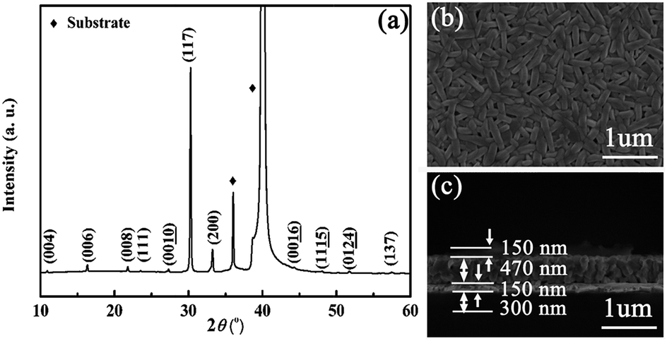 | ||
| Fig. 1 Microstructure characteristics of BNTM thin films: (a) XRD patterns; (b) SEM image for surface; (c) SEM image for cross-section. | ||
Electrical properties
The P–V hysteresis loops of BNTM at low and elevated temperatures measured with the maximum voltage (Vm) of 12 V were shown in Fig. 2(a) and (b). It can be found that the dependences of Vc (Vc = (Vc+ − Vc−)/2) and 2Pr on T (temperature) are strong at low T. The average coercive voltage Vc and 2Pr as a function of T under different Vm were summarized in Fig. 2(c) and (d). At low Vm as shown in Fig. 2(c), Vc first increases and then decreases with increasing T. It is similar to what Wu et al. have reported earlier.22 Moreover, the turning point of T becomes larger with smaller Vm. It can be explained by the relation between the nucleation rate of domains (n) and the activation electric field (α) expressed as n ∝ exp(−α/E). At the condition of low T and small Vm, n is the determining factor for Vc, and n increases with the increasing low T, thus an increasing Vc will be found. For the saturation value of Vm = 16 V, Vc decreases with increasing T. At low T, 2Pr always increases with increasing T and its value changes more slowly with bigger Vm. At elevated temperature as shown in Fig. 2(d), however, 2Pr first decreases with increasing elevated T at saturation value of Vm = 16 V similar to the work found by Zhang et al.23 It is interesting that 2Pr suddenly increases from 425 to 475 K. It can be assumed that a part of mobile charges or ionic vacancies have taken part in the process of polarization switching and it will be verified by impedance spectra analysis below. For the whole range of T, the domain pinning–unpinning competition scenario should work at both low and saturated Vm. This competition has largely depended on the domain wall velocity. The domain wall velocity is controlled by the rate of nucleation (v) which can be expressed as v ∝ exp(−U0/kBT),24 where U0 is the energy barrier for domain nucleation and growth and kB is the Boltzmann constant. It can be seen that the rate of nucleation v increases with increasing T. Thus the larger 2Pr and the smaller Vc at higher temperatures are the results of higher domain wall velocity under the saturation value of Vm. At lower values of Vm, domain pinning is thus considered as the dominant factor that determines the value of Vc. Later, the rate of nucleation v increases strongly with increasing T and domain unpinning becomes the dominant factor. The reason why 2Pr decreases with increasing elevated temperature is due to the larger depolarization field by higher Schottky barrier at film/electrode interfaces as reported by Zhang et al.23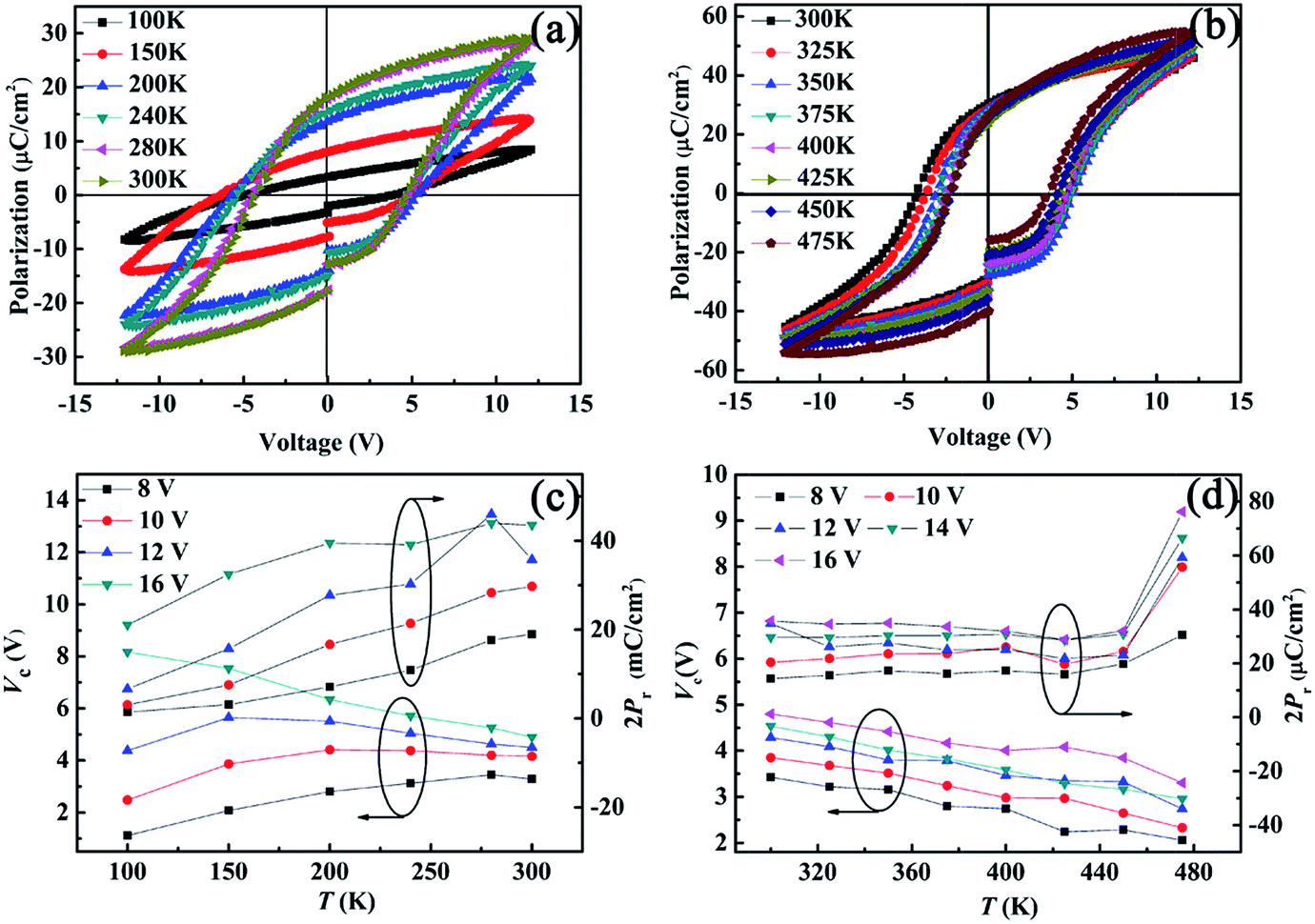 | ||
| Fig. 2 Ferroelectric properties of BNTM thin films: P–V hysteresis loops measured with the Vm of 12 V at 1 kHz and plots of Vc and 2Pr as functions of Vm for (a) and (c) at low temperatures, (b) and (d) at elevated temperatures, respectively. | ||
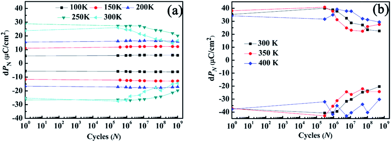
The fatigue characteristics of BNTM thin films at both low and elevated temperatures were displayed in Fig. 3(a) and (b), respectively. Capacitors were switched using a measurement voltage of 10 V and a pulse signal of amplitude of 8 V at 100 kHz. It should be declared that ±dPN =  − (±Pr^)N, where PN is the total polarization, N is the switching cycles,
  is the switched remanent polarization between the two opposite polarity pulses, and Pr^ is the non-switched remanent polarization between the same two polarity pulses. BNTM thin films show no reduction below 200 K. However, the loss of dPN after 109 cycles increased from 28.86% at 250 K to 38.72% at 300 K as shown in Fig. 3(a). It can be seen that the polarization fatigue becomes more serious with increasing T from 100 to 300 K. At elevated T, the reductions of dPN were 41.20% at 300 K, 31.16% at 350 K, and 15.70% at 400 K, respectively. With increasing elevated T, BNTM films show improved fatigue resistance. The improved fatigue properties of BNTM at low T below 200 K can be explained by the weaker effect of domain wall pinning and unpinning.25,26 The low density domain walls at low T can suppress the domain pinning and make the diffusion of defects and charges more difficult. Thus the dependence of fatigue behaviors on T is weak. As temperature increase from 200 to 300 K, the effect of domain wall pinning and unpinning becomes more obvious. At first, the domain pinning is the dominant factor and the polarization fatigue effect is more serious from 250 to 300 K. Since the Schottky barrier at film/electrode interfaces increases with T,23,27 more highly mobile defect charges will be produced by electron injection, which facilitate domain pinning and polarization fatigue.
 | ||
| Fig. 3 Polarization fatigue curves of BNTM thin films (a) at low temperatures and (b) at elevated temperatures. | ||
In order to study the conductance mechanism of fresh and fatigued BNTM thin films at elevated T, ac impedance spectra tests were conducted in the frequency range of 1 kHz to 1 MHz and in the T range from 300 to 475 K. Variations of real and imaginary impedance (Z′ and Z′′) with frequency at different T were shown in Fig. 4(a) and (b), respectively, similarly to the results obtained by Pintilie et al.28 High frequency arcs were ascribed to the grain contribution. The resistances of grains (Rg) of BNTM films were estimated by nonlinear least square fitting with the aid of the program Z-view.29 It can be seen that the value of Rg decreases with increasing elevated T. The Rg follows Arrhenius' relationship as Rg ∝ exp(−Ea/kBT), where kB is the Boltzmann's constant, and Ea is the average activation energy for the conduction process.30 The plot of ln(Rg) vs. 1000/T was presented in Fig. 4(c), which can be clearly divided into three sections with fitting activation energies Ea of 0.01 eV and 0.03 eV from 300 to 375 K, 0.1 eV and 0.09 eV from 375 to 425 K, 0.18 eV and 0.2 eV from 425 to 475 K, for fresh and fatigued condition, respectively. The small value of Ea (0.01–0.03 eV), which was also reported by other authors,31,32 indicates that polarization fatigue has only a slight T dependence for polarization fatigue from 300 to 375 K. The large value of Ea (0.18–0.2 eV) was estimated to be the binding energy for the diffusion of oxygen vacancy within their clusters.33,34 It has been found that the value of Ea increases a little after 1.6 × 10⁹ pulse cycles, which can be ascribed to the charge aggregation at the film/electrode interface11 or at 90° domain walls.35 Thus long-range diffusion of defects and charges happens easily above 380 K (as shown in Fig. 4(c)). Then the combination of small density of oxygen vacancy and high rate of domain nucleation makes the domain pinning more difficult in the body of thin films. However, high Schottky barriers at high temperatures can induce more electron injection and increase the thickness of passive layer at film/electrode interfaces. This was further verified by the fact that the dielectric constant (εr) of BNTM films at 400 K reduces 14.39% after 1 × 10⁹ cycles pulse switching as compared to reductions of 9.76% at 350 K and 8.29% at 300 K under the frequency of 100 kHz (as shown in Fig. 4(d)). So there is also a competition between the body and the interface of the thin film for domain pinning and unpinning. The domain unpinning effect of the body induced by less density of oxygen vacancy and the high rate of domain nucleation leads to an improved fatigue endurance at elevated temperatures.
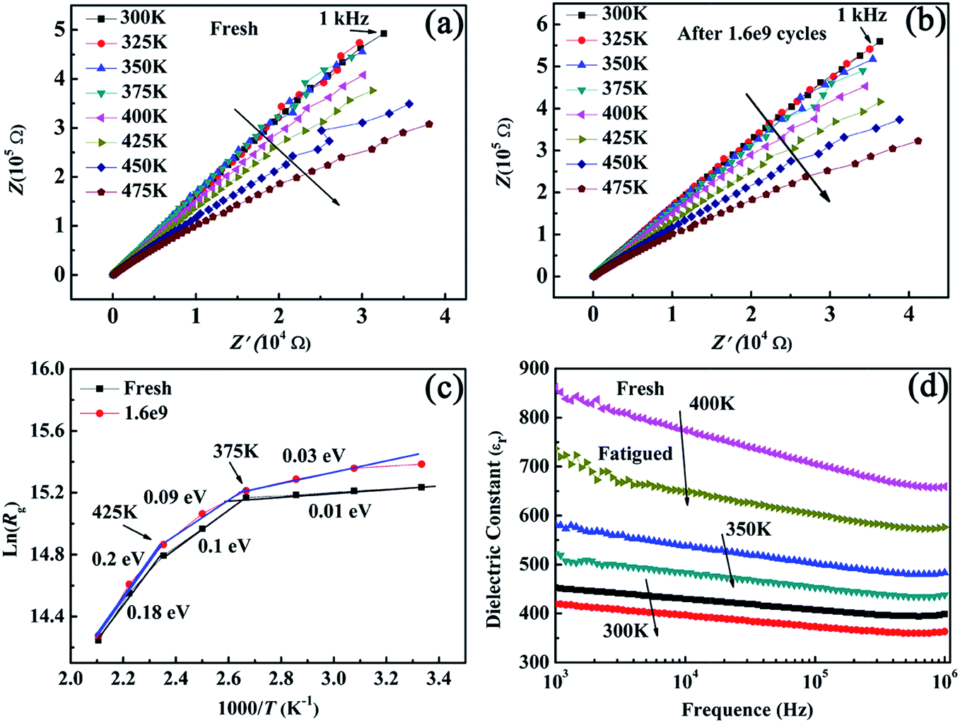 | ||
| Fig. 4 Impedance spectra and dielectric constant analysis of BNTM thin films at elevated temperature: (a) fresh, (b) fatigued after 1.6 × 10⁹ pulse cycles and (c) ln(Rg) vs. 1000/T Arrhenius plots at both fresh and fatigued condition; (d) the dielectric constant (εr) vs. frequency at both fresh and fatigued condition. | ||
The PFM method was also used to study the microscopic domain structures of BNTM thin films (as shown in Fig. 5). It can be found that the surface topography in Fig. 5(a) shows rod-like grains consistent with the image in Fig. 1(b). PFM amplitude of the film was shown in Fig. 5(b). It is obvious that most of the grains show good piezoelectric properties. As for (117)-oriented rod-like grains marked by point A and B, clear PFM amplitude-voltage butterfly loops and phase-voltage hysteresis loops of point A and B were obtained (as shown in Fig. 5(c)). It is found that the grains contained point A and B have 180° phase and high amplitude under a sweep voltage of 15 V. The out-plane (OP) and in-plane (IP) PFM phase images of the film were shown in Fig. 5(d) and (e), respectively. It can be seen in Fig. 5(d) and (e) that piezoelectric polarities marked as white and purple regions are randomly distributed throughout the film surface. The bright and dark regions in OP phase images are correlated with vertically up or down 180°-domain, while the rich yellow and dark regions in IP image are correlated with laterally right or left 90°-domain. Some adjacent grains of two neighboring grains merge into one domain as shown in the grains marked by the point A in Fig. 5(e) and (f), which reveals that there is an indecisive correlation between grains and domains.36 It is interesting that there are two different directions of domain for (117)-oriented grains marked by A, B, C, and D, which should be induced by ferroelastic distortion or internal stress.37
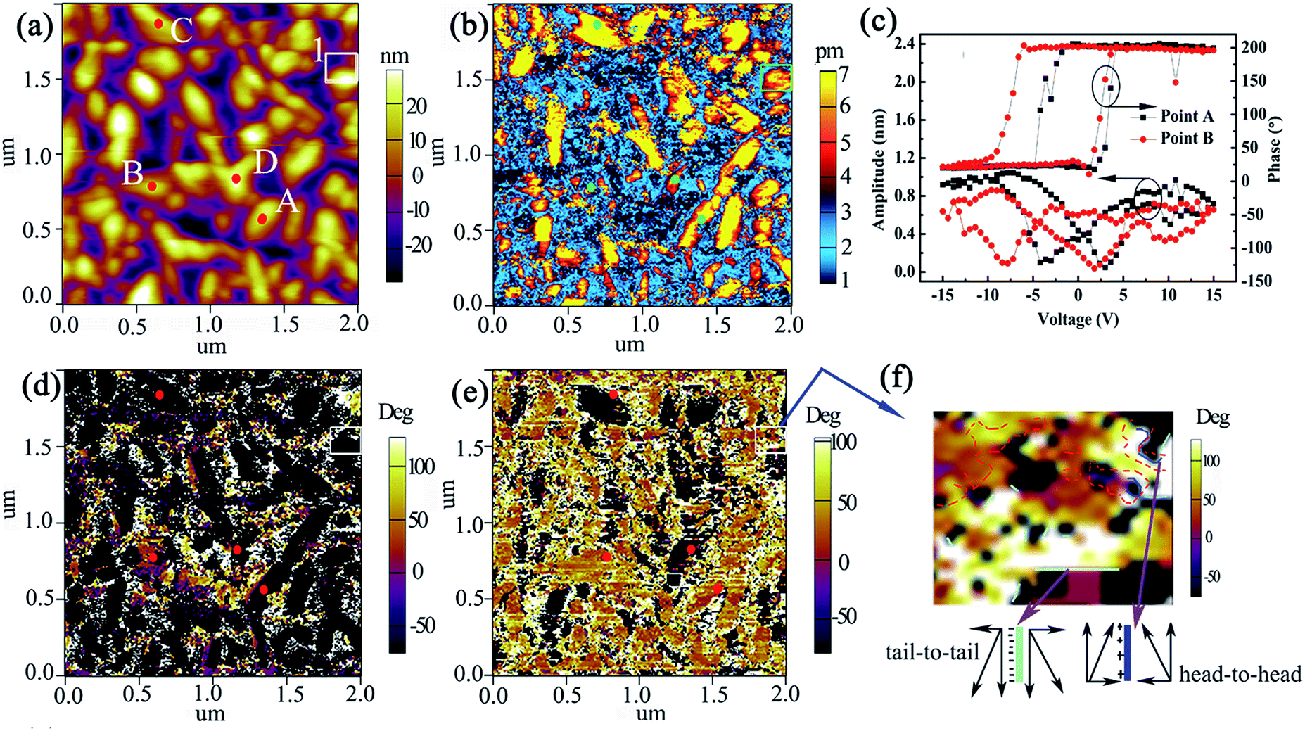 | ||
| Fig. 5 PFM images of BNTM thin films: (a) surface topography; (b) PFM amplitude; (c) the PFM amplitude-voltage butterfly loops and phase-voltage hysteresis loops of point A and point B in (a); (d) OP PFM phase image; (e) IP PFM phase image; (f) zoomed-in IP PFM image of region 1 in white solid square as shown in (a), (d) and (e). The red dotted lines correspond to the bright regions and outside it are dark regions for the same region of OP phase image. The soft sky-blue and dark blue solid lines are non-neutral domain walls of tail-to-tail and head-to-head polarization configuration. | ||
In order to elucidate the domains and the domain walls in detail, a region 1 with white solid square of IP image was zoomed in as shown in Fig. 5(f). The red dotted lines correspond to the bright regions and outside it are dark regions for OP phase image in region 1. The negatively charged domain walls are marked by soft sky-blue solid lines which were induced by tail-to-tail polarization configuration. In the same way, the positively charged domain walls caused by head-to-head polarization configuration are marked by blue solid lines. For both negatively and positively charged domain walls, they are unstable unless mobile carriers such as injected electrons or oxygen vacancies are captured to form a pinned electro-neutral structure.10,11,34,37 Thus both injected electrons at the film/electrode interface and oxygen vacancies in the body of the film can move to the non-neutral domain walls and lead to domain pinning. At low T, both Schottky barriers and density of oxygen vacancies are low and then domain pinning is suppressed. Therefore there is no polarization fatigue. As the temperature increases from 200 to 300 K, the amount of 180°-domain and 90°-domain increases and a higher Schottky barrier induces more electron injection that are captured by non-neutral structure, which can facilitate the polarization fatigue. However, at elevated temperatures, the higher domain wall velocity and less possibility, as compared to those at lower temperatures, for non-neutral domain walls to capture oxygen vacancies in the body of the film realize the improved fatigue. And all the mechanisms at both low and elevated T were summarized in Table 1. It can be seen that the primary mechanism can be change with increasing T and some mechanisms work together to determine the temperature-dependent polarization switching and fatigue properties.
| Mechanisms | Polarization fatigue | ||
|---|---|---|---|
| 100–200 K no obvious fatigue | 200–300 K decline with the increasing T | 300–400 K be better with the increasing T | |
| Domain pinning | Weak | Primary | Secondary |
| Domain unpinning | Weak | Secondary | Primary |
| Schottky barrier induced electron injection | Secondary | Secondary | Secondary |
| Passive layer | Weak | Secondary | Secondary |
| Long-range diffusion of defects and charges | Weak | Weak | Primary |
| The nucleation rate of domains | Primary | Weak | Weak |
Conclusions
In summary, polarization switching and fatigue properties of highly (117)-oriented BNTM ferroelectric thin films were studied at both low and elevated temperatures (100 K up to 475 K). BNTM thin films showed no fatigue properties below 200 K due to the weak effect of domain wall pinning and unpinning. In the temperature range of 200 to 300 K, the polarization fatigue of BNTM films become exacerbated, which can be ascribed to the increasing domain pinning effect and more electron injection from the Schottky barrier at film/electrode interfaces. However, at elevated temperatures from 300 to 400 K, the BNTM films showed improved fatigue endurance with the increasing T. The long-range diffusion of oxygen vacancy within their clusters has been proposed on the fatigue properties of BNTM by temperature-dependent ac impedance spectra analysis. Therefore the oxygen vacancy's redistribution (less density of oxygen vacancy in the body of the film as compared to that at lower temperatures) and strong domain unpinning effect of body of the film induced a better fatigue endurance. Moreover, non-neutral domain walls induced by head-to-head or tail-to-tail polarization configurations were found by PFM phase images. It can be assumed that both injected electrons at the film/electrode interface and oxygen vacancies in the body of the film can move to the non-neutral domain walls and lead to domain pinning. These results may be useful for applications of layered perovskite structure ferroelectric films in a broad temperature range.Acknowledgements
This work was financially supported by the Project of National Natural Science Foundation of China (NSFC) (Grant No. 51472210 and 61404113), Hunan Provincial Innovation Foundation for Postgraduate Grant No. CX2014B267.Notes and references
- D. Xie, Y. F. Luo, X. G. Han, T. L. Ren and L. T. Liu, J. Appl. Phys., 2009, 106, 4117 Search PubMed.
- H. J. Song, T. Ding, X. L. Zhong, J. B. Wang, B. Li, Y. Zhang and Y. C. Zhou, RSC Adv., 2014, 4, 60497 RSC.
- S. G. Yuan, J. B. Wang, X. L. Zhong, F. Wang, B. Li and Y. C. Zhou, J. Mater. Chem. C, 2013, 1, 418 RSC.
- Z. H. Tang, Y. Xiong, M. H. Tang, Y. G. Xiao, W. Zhang, M. L. Yuan, J. Ouyang and Y. C. Zhou, J. Mater. Chem. C, 2014, 2, 1427 RSC.
- A. K. Tagantsev, I. Stolichnov, E. L. Colla and N. Setter, J. Appl. Phys., 2001, 90, 1387 CrossRef CAS.
- J. F. Scott and M. Dawber, Appl. Phys. Lett., 2000, 76, 3801 CrossRef CAS.
- P. K. Larsen, G. J. M. Dormans, D. J. Taylor and P. J. Van Veldhoven, J. Appl. Phys., 1994, 76, 2405 CrossRef CAS.
- X. J. Lou, M. Zhang, S. A. T. Redfern and J. F. Scott, Phys. Rev. B: Condens. Matter Mater. Phys., 2007, 75, 224104 CrossRef.
- N. Zhong, P. H. Xiang, Y. Y. Zhang, X. Wu, X. D. Tang, P. X. Yang, C. G. Chun and J. H. Chu, J. Appl. Phys., 2015, 118, 104102 CrossRef.
- S. H. Baek, C. M. Folkman, J. W. Park, S. Lee, C. W. Bark, T. Tybell and C. B. Eom, Adv. Mater., 2011, 23, 1621 CrossRef CAS PubMed.
- X. Zou, L. You, W. Chen, H. Ding, D. Wu, T. Wu, L. Chen and J. L. Wang, ACS Nano, 2012, 6, 8997 CrossRef CAS PubMed.
- H. Guo, X. Liu, J. Rödel and X. Tan, Adv. Funct. Mater., 2015, 25, 270 CrossRef CAS.
- U. Chon, H. M. Jang, M. G. Kim and C. H. Chang, Phys. Rev. Lett., 2002, 89, 087601 CrossRef PubMed.
- Y. Qiao, C. J. Lu, Y. J. Qi and Y. H. Zhou, Phys. B, 2008, 403, 2488 CrossRef CAS.
- X. L. Zhong, J. B. Wang, M. Liao, C. B. Tan, H. B. Shu and Y. C. Zhou, Thin Solid Films, 2008, 516, 8240 CrossRef CAS.
- W. L. Zhang, M. H. Tang, Y. Xiong, K. Wang, Z. P. Wang, Y. G. Xiao, S. A. Yan, Z. Li and J. He, RSC Adv., 2016, 6, 88668 RSC.
- W. L. Zhang, M. H. Tang, Y. Xiong, Z. P. Wang, Y. G. Xiao, S. A. Yan, Z. Li and J. He, J. Sol-Gel Sci. Technol., 2016, 80, 853 CrossRef CAS.
- C. Zhao, D. Wu, A. D. Li and Y. D. Xia, J. Phys. D: Appl. Phys., 2008, 41, 122003 CrossRef.
- F. Yang, Y. C. Guo, L. Y. Li and M. H. Tang, J. Phys. D: Appl. Phys., 2016, 49, 195305 CrossRef.
- G. D. Hu, J. Appl. Phys., 2006, 100, 6109 Search PubMed.
- H. N. Lee, D. Hesse, N. Zakharov and U. Gosele, Science, 2002, 296, 2006 CrossRef CAS PubMed.
- D. Wu, G. L. Yuan and A. D. Li, Appl. Phys. Lett., 2007, 90, 062902 CrossRef.
- Y. Zhang, X. L. Zhong, Z. H. Chen, J. B. Wang and Y. C. Zhou, J. Appl. Phys., 2011, 110, 014102 CrossRef.
- C. Miller and G. Weinreich, Phys. Rev., 1960, 117, 1460 CrossRef.
- G. L. Yuan, J. M. Liu, Y. P. Wang, D. Wu, S. T. Zhang, Q. Y. Shao and Z. G. Liu, Appl. Phys. Lett., 2004, 84, 3352 CrossRef CAS.
- Y. Wang, K. F. Wang, C. Zhu and J. M. Liu, J. Appl. Phys., 2006, 99, 044109 CrossRef.
- Y. Zhou, X. Zou, L. You, R. Guo, Z. Shiuh Lim, L. Chen, G. L. Yuan and J. L. Wang, Appl. Phys. Lett., 2014, 104, 012903 CrossRef.
- L. Pintilie, L. Hrib, I. Pasuk, C. Ghica, A. Iuga and I. Pintilie, J. Appl. Phys., 2014, 116, 044108 CrossRef.
- J. H. Park, J. S. Bae, B. C. Choi and J. H. Jeong, J. Phys. D: Appl. Phys., 2007, 40, 579 CrossRef CAS.
- Y. H. Lin, J. Cai, M. Li, C. W. Nan and J. He, J. Appl. Phys., 2008, 103, 074111 CrossRef.
- T. Mihara, H. Watanabem and C. A. P. de Araujo, Jpn. J. Appl. Phys., Part 1, 1994, 33, 3996 CrossRef CAS.
- B. H. Wen, Y. Zhang, X. L. Liu, L. Ma and X. R. Wang, J. Mater. Sci., 2012, 47, 4299 CrossRef CAS.
- Q. Q. Ke, X. J. Lou, Y. Wang and J. Wang, Phys. Rev. B: Condens. Matter Mater. Phys., 2010, 82, 024102 CrossRef.
- Q. Q. Ke, A. Kumar, X. J. Lou, Y. P. Feng, K. Y. Zeng, Y. Q. Cai and J. Wang, Acta Mater., 2015, 82, 190 CrossRef CAS.
- Y. Kitanaka, Y. Noguchi and M. Miyayama, Phys. Rev. B: Condens. Matter Mater. Phys., 2010, 81, 094114 CrossRef.
- A. Gruvermana, O. Auciello and H. Tokumoto, Appl. Phys. Lett., 1996, 69, 3191 CrossRef.
- S. Katayama, Y. Noguchi and M. Miyayama, Adv. Mater., 2007, 19, 2552 CrossRef CAS.
| This journal is © The Royal Society of Chemistry 2017 |