
 Open Access Article
 This Open Access Article is licensed under a Creative Commons Attribution-Non Commercial 3.0 Unported Licence
ZnO films using a precursor solution irradiated with an electron beam as the cathode interfacial layer in inverted polymer solar cells†
Rira Kanga,
Yong-Jin Nohb,
Jin-Mun Yuna,
Hyun Kima,
NoSoung Myoungd,
Eun-Hye Leec,
Tae-Wook Kim c,
Seok-In Na‡
*b and
Seung-Hwan Oh‡*a
c,
Seok-In Na‡
*b and
Seung-Hwan Oh‡*a
aRadiation Research Division for Industry and Environment, Korea Atomic Energy Research Institute (KAERI), 29 Geumgu-gil, Jeongeup-si, Jeollabuk-do 580-185, Republic of Korea. E-mail: ohsh@kaeri.re.kr
bProfessional Graduate School of Flexible and Printable Electronics, Polymer Materials Fusion Research Center, Chonbuk National University, 664-14, Deokjin-dong, Jeonju-si, Jeollabuk-do 561-756, Republic of Korea. E-mail: nsi12@jbnu.ac.kr
cAdvanced Photonics Research Institute (APRI), Gwangju Institute of Science and Technology (GIST), Gwangju 61005, Republic of Korea
dSoft Innovative Materials Research Center, Institute of Advanced Composite Materials, Korea Institute of Science and Technology, Joellabuk-do 565-905, Republic of Korea
First published on 18th May 2017
Abstract
We demonstrate the possibility of irradiating sol–gel ZnO with an electron beam (EB-ZnO) to modify sol–gel ZnO, and EB-ZnO is explored as a cathode interfacial layer for inverted polymer solar cells. We investigate the effect of EB-ZnO on the surface, optical and electric properties of sol–gel ZnO films through morphology, chemical composition, optical band gap shift, various defect excitations (photoluminescence) and work function measurement. Oxygen vacancies and the formation of nitrogen on the surface of EB-ZnO films contribute to the formation of n-type degenerated EB-ZnO films. The electric properties of EB-ZnO strongly depend on the adsorbed dose, and EB-ZnO with a suitable dose of 100 kGy improved the power conversion efficiency of inverted polymer solar cells based on PTB7-Th: PC71BM from 8.05% for non-treated sol–gel ZnO to 9.36% for EB-ZnO with an enhanced fill factor.
Introduction
Polymer solar cells (PSCs) have attracted considerable attention due to their low cost, light weight, flexibility, environmentally friendly energy sources.1–7 Various strategies (low band gap donors,1,2 novel acceptors,3,4 new device configurations,5,6 and interface engineering7,8) have been rapidly developed to improve their power conversion efficiency (PCE). Recently, PSCs with low band gap donors have achieved PCE greater than 10%.1,2 The inverted device configuration in polymer solar cells (ITO/cathode interfacial layer/active layer/anode interfacial layer/Ag) has been widely used due to its higher PCEs and longer lifetimes than that of the conventional configuration.9In inverted PSCs, a cathode interfacial layer (CIL) such as metal oxide (ZnO, TiOx and Cs2CO3) and conjugated polymers is required to change the polarity of ITO to a cathode.7,10,11 Among them, sol–gel ZnO has been the most commonly used material as a CIL due to its (1) high transparency, (2) suitable energy level (conduction band: −4.4 eV and valence band: −7.8 eV) for electron collection and hole blocking, (3) good electron mobility, and (4) easy solution processing.10–12 However, the widely used sol–gel ZnO exhibits many surface defects/traps, such as dangling bonds and adsorbed oxygen on its surface due to low temperature solution processing.11 Such defects act as recombination centers and lead to poor device performances in PSCs. To overcome these problems, many approaches such as control of morphology, modification of nanostructure, doping and surface modification with self-assembly layer or polymers bilayer have been developed for better electron collection.10–12
As a promising new approach, techniques based on various types of ionizing radiation (alpha, electron beam, gamma rays, X-rays, laser ablation, α-particles, neutrons, protons, and ion beams) for the fabrication and synthesis of materials are becoming useful.13,14 The high energy of electron beam leads to the formation of radicals within a short time.14 Especially, the effect of electron-beam irradiation on the electrical and optical properties of ZnO was recently investigated. K. P. Sapnar et al. synthesized ZnO nanoparticles (NPs) via microwave, and the ZnO NPs powder was exposed to electron irradiation, which resulted in an increase in their bandgap and reduction of the NPs size.15 J. S. Bhat et al. observed an increase in sheet resistance, blue shift in the absorption edge and decrease in structural homogeneity and crystalline size after sol–gel ZnO and ZnO:Al films were exposed to electron irradiation.16 The results of such research indicate that electron beam irradiation could induce defects and modify electronic and optical properties, regardless of the phase of ZnO (films or powder). However, to the best of our knowledge, the application of ZnO exposed to electron irradiation in solar cells has not yet been reported.
Hence, sol–gel ZnO irradiated with an electron beam was developed as a CIL in inverted polymer solar cells with a device structure of ITO/electron-beam based sol–gel ZnO (EB-ZnO)/PTB7-Th:PC71BM/MoO3/Ag. Herein, the application of EB-ZnO as a cathode interfacial in PSCs is first reported. We directly irradiate the sol–gel ZnO precursor solution with an electron beam as a function of adsorbed dose (100, 300 and 500 kGy), and use ZnO films spin-coated from the irradiated solution as a CIL in inverted PSCs. This electron irradiation makes the sol–gel ZnO n-type degenerated by inducing oxygen vacancies, which can increase electron concentrations; and their surface composition, morphology, photoluminescence, energy-level diagram are investigated to understand the fundamentals of the changed properties of EB-ZnO. The inverted PSCs with EB-ZnO at 100 kGy exhibit the best power conversion efficiency (PCE) of 9.36% due to the enhanced fill factor of 71.8%. In addition, the device with EB-ZnO at 100 kGy exhibits the lowest series resistance and dominant bimolecular recombination.
Experimental
Preparation of irradiated sol–gel ZnO with electron beam (EB-ZnO)
Sol–gel ZnO was prepared according to a previous report.17 Next, 20 mL sol–gel ZnO in a glass vial was irradiated at room temperature with electron-beam irradiation at a scan rate of 10 kGy min−1 created by 2.5 MeV UELV-10-10S electron accelerator at the Korea Atomic Energy Research Institute (ex. 2.5 MeV × 5.8 mA × 10 m min−1 × 1 turn = 10 kGy). The total absorbed doses were 100, 300 and 500 kGy. The untreated sol–gel ZnO and sol–gel ZnO irradiated with electron beam at 100, 300 and 500 kGy are denoted as Ref, EB-Z100, EB-Z300 and EB-Z500, respectively.Fabrication and characterization of inverted polymer solar cells
To fabricate the device, ITO coated glass was cleaned with acetone, DI water and IPA, dried in an oven, and UV-ozone treated for 20 min. EB-ZnO was spin-coated onto ITO, at a thickness of ∼60 nm, followed by drying at 150 °C for 30 min under air. As the active layer, a blend solution film of 12 mg of PTB7-Th (1-material) and 18 mg of PC71BM (1-material) in 1 mL of chlorobenzene with 5% (v/v) the additive DIO was then spin-coated onto EB-ZnO at 2000 rpm for 60 s in an N2-filled glove box. Under the vacuum of 10−6 torr, 3 nm MoO3 was thermally evaporated onto the active layer, and then 80 nm-thick silver as the anode electrode was thermally deposited onto MoO3 through a shadow mask with an area of 4.64 mm2. The photocurrent–voltage (J–V) characteristics of the devices were measured using a Keithley 2400 instrument and solar simulator (Oriel sol3A) under air.Sample characterization
Atomic force microscopy (AFM) (Veeco, Digital Instruments Nanoscope IIIA) in tapping mode was used to characterize the EB-ZnO films spin-coated on Si wafers. X-ray photoelectron spectroscopy (XPS) and ultraviolet photoemission spectroscopy (UPS) measurements (AXIS NOVA, Kratos) were carried out for the EB-ZnO films spin-coated on ITO substrates (monochromatized Al Kα for XPS, and a He l (hν = 21.2 eV) excitation for UPS at a pressure of 5 × 10⁻⁸ torr). The UV-vis spectra of spin-coated EB-ZnO films spin-coated on glass substrates were recorded using a spectrophotometer. Photoluminescence (PL) spectra of EB-ZnO films spin-coated on glass substrates were measured via the 2nd harmonic generation (at 350 nm) of a mode-locked Ti:Sapphire laser (Chameleon Ultra II coherent) at 300 K. Transmission electron microscopy (TEM) was used to investigate the crystalline size of EB-ZnO (Titan 80-300, FEI, operated at 300 kV). For the characterization, the EB-ZnO films were prepared via the same procedures as that for device fabrication.Result and discussion
Surface properties
Fig. 1a shows a photograph of the actual solutions of Ref, EB-Z100, EB-Z300 and EB-Z500. With an increase in the adsorbed dose from 100 to 500 kGy, the color of the EB-ZnO solution changed from transparent to orange-red. To observe the differences in surface properties between all the samples, as shown in Fig. 1b, the morphologies of the Ref and EB-ZnO samples were investigated via atomic force microscopy (AFM). All the samples exhibit flat surfaces without a ripple type morphology, which is probably due to the low-temperature annealing. EB-Z100 a slightly reduced surface roughness compared with that of Ref; whereas EB-Z500 shows a rough surface with a random distribution of particles. The increase in surface roughness suggests that electrons cannot be collected beneficially to the cathode. To observe the change in the crystalline size of EB-ZnO, the EB-ZnO samples were characterized using TEM. Unexpectedly, there was no significant change in all the samples (crystalline size: about 0.23 nm in Fig. S1†).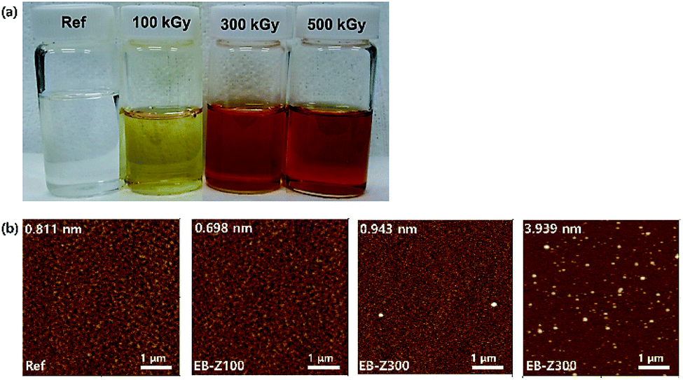 | ||
| Fig. 1 (a) Photograph of the Ref and EB-ZnO precursor solutions and (b) AFM images of the Ref and EB-ZnO films with a size of 5 × 5 μm2. The upper left value is the root-mean-square (RMS) in the AFM images. | ||
In order to obtain information about the surface of EB-ZnO, XPS analysis was carried out on EB-ZnO. The binding energies were calibrated with respect to the C 1s peak at 258.0 eV. As shown in Fig. 2, the O 1s peaks can be deconvoluted into three Gaussian components (Oa: O2− ions in the ZnO lattice, Ob: O2− ions in the oxygen vacancy of ZnO and Oc: chemisorbed oxygen species on the surface of ZnO).18 For better comparison, the content and peak positions of each O 1s component are shown in Fig. 2. The O 1s peaks of Ref are centered at 530.6 eV (Oa: 63.8%), 531.5 eV (Ob: 7.7%) and 531.9 eV (Oc: 28.5%). With the increase in the irradiation dose, the O 1s peaks broaden and shift toward lower binding energies by 0.4, 0.9 and 0.7 eV, and the content of Ob increases to 43.3%, 80.1% and 58.0% for EB-Z100, EB-Z300 and EB-Z500, respectively. It is known that such oxygen vacancy can act as donors, which lead to degenerate ZnO by increasing the electron carrier density in the conduction band (CB) of ZnO. Moreover, the content of Oc decreases to 12.0%, 1.3% and 1.9% for EB-Z100, EB-Z300 and EB-Z500, respectively. The surface hydroxyl groups trap photoinduced electrons and holes, thus enhancing the photocatalytic degradation process. It is noted that electron beam irradiation can induce oxygen vacancies and reduce surface hydroxyl groups of sol–gel ZnO.34
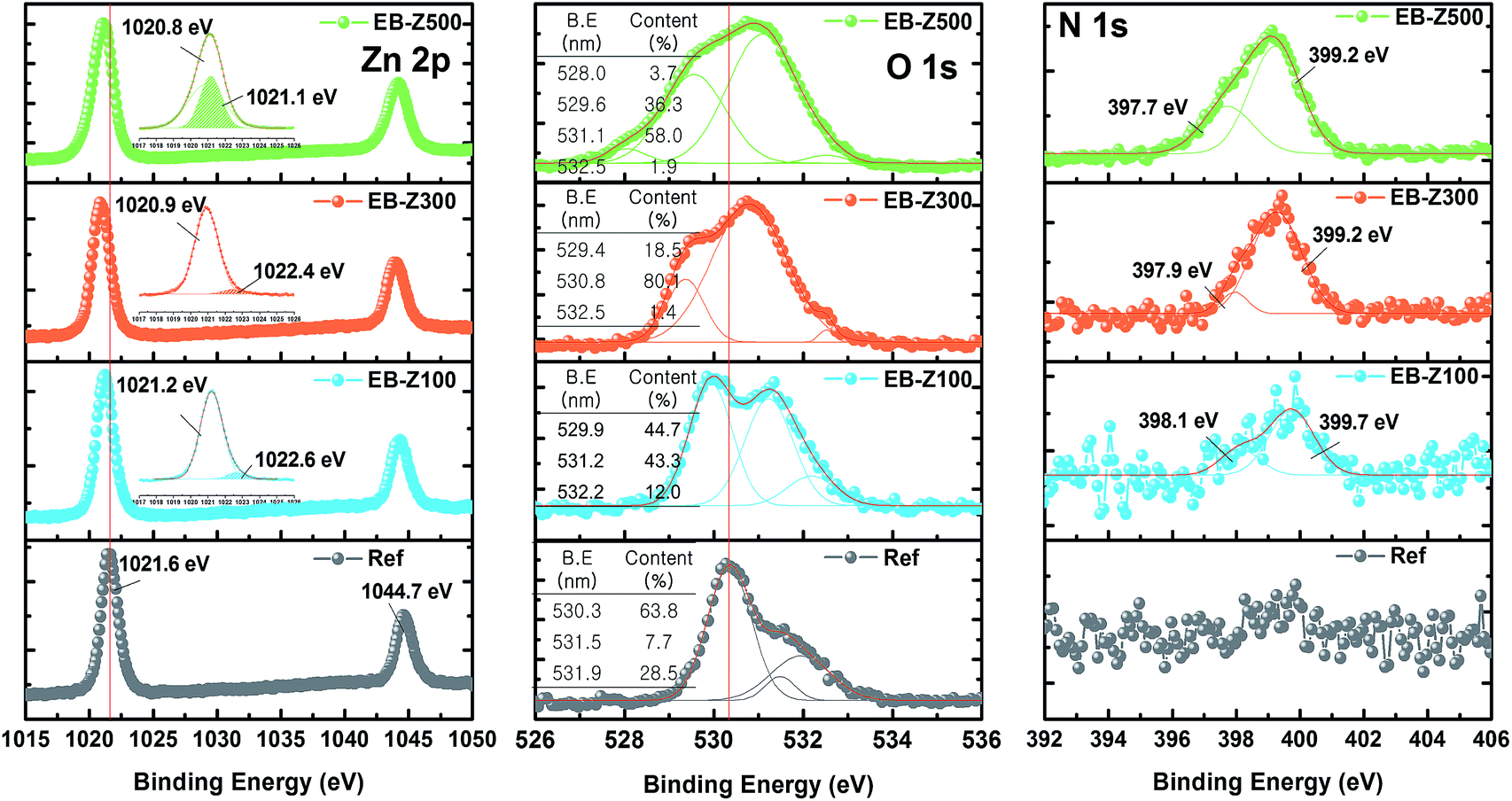 | ||
| Fig. 2 Zn 2p, O 1s, and N 1s XPS spectra of Ref, EB-Z100, EB-Z300 and EB-Z500 (inset in the O 1s XPS spectra is the content of oxygen species calculated from O 1s fitting spectra). | ||
For all samples, Zn 2p has doublet peaks (for the non-treated ZnO, Zn 2p3/2: 1021.6 eV and Zn 2p1/2: 1044.7 eV). The Zn 2p peak shifts toward a lower binding energy by 0.4, 0.7 and 0.8 eV for EB-Z100, EB-Z300 and EB-Z500, respectively, similarly to the shift of the O 1s peak. FWHM (full width at half maximum) can be an indicator of chemical state changes and physical influence. With the increase in irradiation dose, Zn 2p FWHM broadening occurs (Ref: 1.456, EB-Z100: 1.497, EB-Z300: 1.551 and EB-Z500: 1.776), and additional peaks are also observed at higher biding energies (the shaded area of the insets in Fig. 2). This result can be attributed to the presence of zinc interstitial (Zni).19 It is reported that Zni can degenerate ZnO by acting as donors and can interact with adjacent active layers with respect to the stability of polymer solar cells.35
Interestingly, we also observed N 1s spectra in the EB-ZnO samples, but not in Ref. The N 1s of EB-Z100 can be deconvoluted into two peaks at 398.1 and 399.7 eV, which are attributed to –C![[double bond, length as m-dash]](https://www.rsc.org/images/entities/char_e001.gif) N– and –NH–C or N–(C)3, respectively.20 Given the content of Ob for the EB-ZnO samples, it is expected that N atoms do not occupy the O sites in our study (i.e., N–Zn bonds is not observed). The two peaks of EB-Z300 and EB-Z500 slightly shift toward lower binding energies, which contributes to the enhanced electron concentration of the modified EB-ZnO surface by the interaction between different types of amines and ZnO. Although the origin of N formation on the EB-ZnO surface is not clear, it can originate from the byproduct (NH4+) related to the degradation of ethanolamine21 or unstable intermediate products such as OH˙ and H˙ radicals by electron beam irradiation.13 It can be suggested that the byproducts, unstable intermediate products and reactants from the ZnO precursor solution, which are not volatile at 150 °C, are adsorbed on the surface of ZnO.
N– and –NH–C or N–(C)3, respectively.20 Given the content of Ob for the EB-ZnO samples, it is expected that N atoms do not occupy the O sites in our study (i.e., N–Zn bonds is not observed). The two peaks of EB-Z300 and EB-Z500 slightly shift toward lower binding energies, which contributes to the enhanced electron concentration of the modified EB-ZnO surface by the interaction between different types of amines and ZnO. Although the origin of N formation on the EB-ZnO surface is not clear, it can originate from the byproduct (NH4+) related to the degradation of ethanolamine21 or unstable intermediate products such as OH˙ and H˙ radicals by electron beam irradiation.13 It can be suggested that the byproducts, unstable intermediate products and reactants from the ZnO precursor solution, which are not volatile at 150 °C, are adsorbed on the surface of ZnO.
Optical properties
The optical properties of the samples were investigated, as shown in Fig. 3a and b. The band gaps (Eg) of EB-ZnO were estimated from the (αhν)2 vs. hν plot (Tauc plot extrapolation). The band gap is estimated to be 3.33, 3.36, 3.38 and 3.37 eV for Ref, EB-Z100, EB-Z300 and EB-Z500, respectively (refer to Table 2 and Fig. 2a). The absorption spectra of samples are presented in Fig. 2b. All the EB-ZnO samples show UV absorption and transparency in the visible region and with the increase in absorption dose, their band gaps increase. The EB-Z500 sample is significantly blue shifted compared to the other samples. The band gap widening of the EB-ZnO samples is probably due to the well-known Burstein–Moss effect (BM effect), which is related to heavily doped/degenerated semiconductors. The BM effect is the phenomenon in which doping causes a Fermi level (Ef) shift above the conduction band, i.e. since electrons fill up all the states below Ef, the optical band gap increases.22,23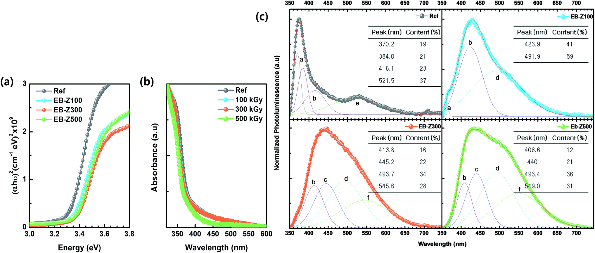 | ||
| Fig. 3 (a) Tauc plot, (b) UV-vis spectra and (c) normalized photoluminescence (PL) spectra of Ref, EB-Z100, EB-Z300 and EB-Z500. PL spectra were deconvoluted into Gaussian peaks (a to f correspond to Table 1 and Scheme 1). | ||
| Related defects | Interband (nm, eV) | Zni, VZn, Oi (nm, eV) |
|
OZn | Oi, VO | |
|---|---|---|---|---|---|---|
| Color | Violet | Blue | Sky blue | Green | ||
| Ref | 370.2, 3.35 | 416.1, 2.98 | 521.5, 2.38 | |||
| 384.0, 3.23 | ||||||
| EB-Z100 | — | 423.9, 2.93 | 491.9, 2.52 | |||
| EB-Z300 | — | 413.8, 3.00 | 445.2, 2.78 | 493.7, 2.51 | 545.6, 2.27 | |
| EB-Z500 | — | 408.6, 3.03 | 440, 2.81 | 493.4, 2.51 | 549.0, 2.26 | |
| Possible mechanism | (a) | (b) | (c) | (d) | (e) | (f) |
| FX → VB | CB → VZn | ex-Zni → VB |  |
CB → OZn | CB → Oi | |
| CB → VB | Zni → VB | CB → VO | ||||
| CB → Oi |
| Eg (eV) | V.B (eV) | C.B (eV) | W.F (eV) | |
|---|---|---|---|---|
| Ref | 3.33 | 7.56 | 4.23 | 4.12 |
| EB-Z100 | 3.35 | 7.54 | 4.19 | 3.75 |
| EB-Z300 | 3.38 | 7.44 | 4.06 | 3.55 |
| EB-Z500 | 3.37 | 7.44 | 4.07 | 2.99 |
In addition, for the characterization of EB-ZnO defects, the photoluminescence (PL) spectra of samples are shown in Fig. 3c. The Ref sample shows both UV emission and visible emission and EB-Z100 slightly shows UV emission, whereas the other EB-ZnO samples did not show UV emission (red-shifted PL) despite their blue-shifted UV-vis spectra. Such red-shifted PL spectra of EB-ZnO result from the fact that absorption occurs from the valance band to the Ef or the conduction band (CB), whereas luminescence occurs from the impurity-donor band to the valance band (VB) or acceptor-like state.24 Since PL spectra are suitable tools for the characterization of the defects, the PL spectra were deconvoluted into several Gaussian subpeaks. Generally, there are a number of defect states within the bandgap of ZnO (donor defects: zinc interstitial, Zni, and oxygen vacancy, VO, acceptor defects: zinc vacancy, VZn, oxygen interstitial, Oi and oxygen antisite, OZn). It is known that the relative content of donor and acceptors influences the semiconductor properties of ZnO.25
Scheme 1 and Table 1 show the various defects level emissions for the deconvoluted peaks (a to f) of the PL spectra (Fig. 3c). The origin of the PL spectra is complicated, which is due to the fact that PL is mostly related to VO and/or Zni. As mentioned above, the Ref and EB-Z100 samples only exhibit UV emission (peak a), which is due to that free excitons (FX, 0.06 eV below the CB) recombine with holes in the VB.26 With an increase in the absorption dose, the PL spectra display visible region broadening. The violet emission (peak b) displayed in all the samples is probably attributed to (1) Zni (about 0.22 eV below the CB) → VB transition or (2) CB → single ionized VZn (about 0.3 eV above the VB) or (3) CB → Oi (about 0.4 eV above the VB).25–27 The blue emission (peak c) of EB-Z300 and EB-Z500 is due to ex-Zni, which is the extended states of Zni from 0.54 to 0.64 eV below the CB.26,27 This can be correlated to the additional Zn 1p peaks of EB-Z300 and EB-Z500 (the shaded area, inset Fig. 2), where the shaded area of EB-Z500 is significant (inset Fig. 2). For the EB-ZnO samples, the sky blue emission (peak d) results from the process (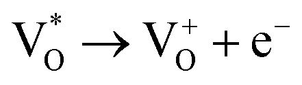 , below the CB) in the grain boundary.26 The increase in the content of Ob for the EB-ZnO samples is evidence of this emission. For only the Ref sample, electron transition from the CB to OZn occurs (peak e).28 The green emission (peak f) of EB-Z300 and EB-500 is due to two possibilities: (1) CB → Oi (about 1.09 eV above the VB) or (2) trap state emissions attributed to the single ionized VO (about 0.90 eV above the VB).27 The PL spectra of EB-Z100 includes two subpeaks (b and d) related to donor defects (Zni and
  ), whereas that of EB-Z300 and EB-Z500 significantly include additional contents (lines d and f) related to both donor and acceptor defects (VZn, Oi and VO). The origin of the PL emission does not seem to clearly correlate with the intrinsic or extrinsic defects due to the extremely complicated defect energy level. However, the presence of ex-Zni and VO is supported by the XPS results, which indicates that oxygen vacancies and Zn interstitial are dependent on the irradiation dose.
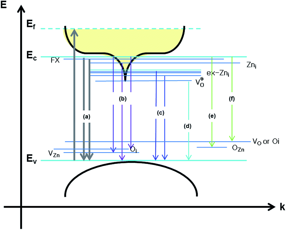 | ||
| Scheme 1 Schematic diagram of the energy band structures of EB-ZnO and photoluminescence mechanism of EB-ZnO corresponding to the data in Table 1. | ||
Electronic properties
To observe the change in energy levels of the EB-ZnO samples, we carried out ultraviolet photoelectron spectroscopy (UPS) measurements (Fig. 4a). Fig. 4b and Table 2 exhibit the energy levels extracted from the UPS results. The work function (W.F, φ) is determined by the distance between the secondary electron edge at high binding energy and HeI energy = 21.2 eV (the left panel in Fig. 4a). The valence band maximum (VBM) was calculated from the onset to the Ef at the low binding energy region (the right panel in Fig. 4a). The conduction band minimum (CBM) was estimated from the VBM and Eg (extracted from the Tauc plot). The Ref samples show a W.F of about 4.12 eV, which is similar with that of previously reported sol–gel ZnO,29 but an Ef slightly above the CB is observed in our study. With the increase in irradiation dose from 100, 300 to 500 kGy, the W.F decreases from 3.75, 3.55 to 2.99 eV, respectively. As mentioned for the bandgap widening of the EB-ZnO samples, the Ef of EB-ZnO samples shifts above the CB (i.e., the EB-ZnO samples are degenerated) from the UPS data. Given both optical properties (the red shift of PL spectra and bandgap broadening) and UPS data, the EB-ZnO samples seem to be heavily n-type doped ZnO. Although N-doped ZnO with N–Zn bonds is known as p-type, in our study, n-type doping of EB-ZnO can be explained by (1) the zinc interstitial and oxygen vacancy as the donor result in band tails, which merge with the CB and cause band broadening,23 or (2) N–C bonds, such as amine groups, adsorbed on the surface can influence the reduction of W.F due to the interfacial dipole, similarly to the previously reported result.30 Unfortunately, in our study, the electron mobility and hole measurement of the Ref and EB-ZnO samples could not be measured probably due to the highly resistive films.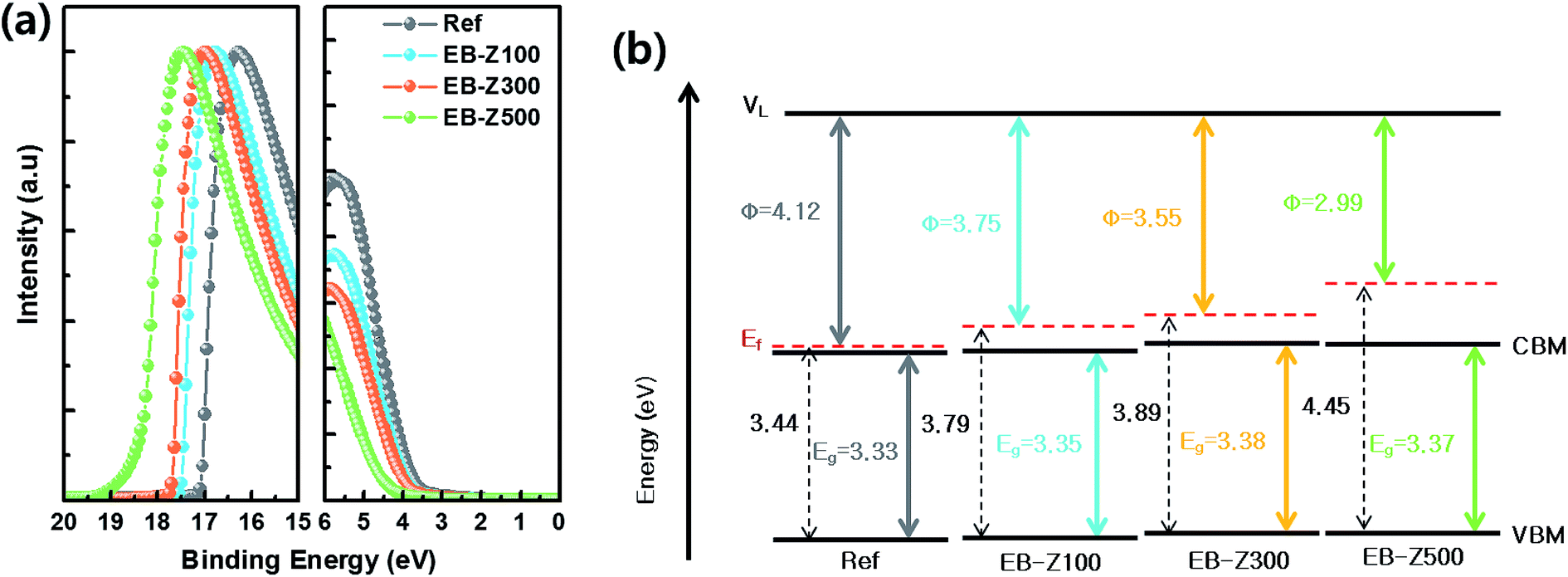 | ||
| Fig. 4 (a) UPS data and (b) corresponding energy diagram of Ref, EB-Z100, EB-Z300 and EB-Z500. | ||
Photovoltaic properties
The photovoltaic properties of the samples were investigated with the device structure of ITO/EB-ZnO/PTB7-Th:PC71BM/MoO3/Ag. The J–V characteristic in a single batch and the average of photovoltaic performance parameters are shown in Fig. 5a–c and Table 3. For the Ref samples, the open circuit voltage (Voc), short circuit current density (Jsc), fill factor (FF) and PCE values were 0.79 V, 15.92 mA cm−2, 64.3% and 8.05%, respectively. When EB-Z100 and EB-Z300 were used, the PCE was significantly enhanced, and the device with EB-Z100 shows the best performance with an FF of 71.8% and PCE of 9.36% (increase of 13%). From the modified W.F, we expected that EB-Z500 would show the best results because the W.F of the samples decreases with the increase in irradiation dose. Interestingly, EB-Z500 shows the lowest PCE and widest distribution of PCE. The external quantum efficiency (EQE) of the same devices is shown in Fig. 5d. The measured Jsc is less than the value calculated from the EQE data (the error is less than 10%). This discrepancy can be due to the difference in illumination conditions.31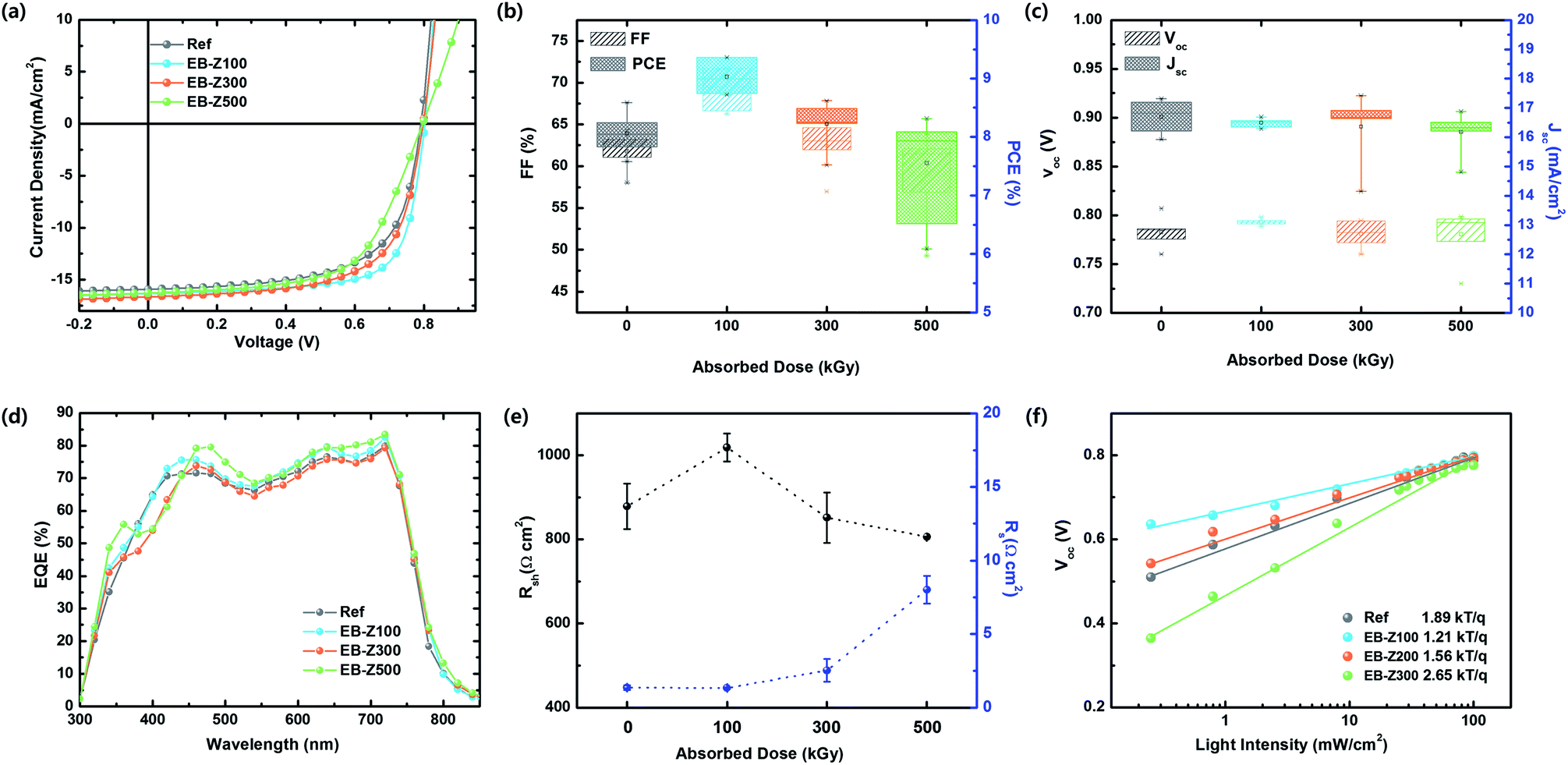 | ||
| Fig. 5 (a) J–V curve, (b) variation in FF and PCE, (c) variation in Voc and Jsc, (d) corresponding EQE data, (e) Rs and Rsh, and (f) Voc dependence on Plight for the PSCs based on ITO/Ref and EB-ZnO/PTB7-Th:PC71BM/MoO3/Ag. | ||
| Sample | Voc (V) | Jsc (mA cm−2) | FF (%) | PCE (%) | EQE Jsc (mA cm−2) | Rs (Ω cm2) | Rsh (Ω cm2) |
|---|---|---|---|---|---|---|---|
| Ref | 0.79 (0.78 ± 0.02) | 15.92 (16.69 ± 0.6) | 64.3 (61.8 ± 2.4) | 8.05 (7.93 ± 0.3) | 17.50 | 1.35 ± 0.15 | 878 ± 54 |
| EB-Z100 | 0.80 (0.79 ± 0.01) | 16.35 (16.49 ± 0.2) | 71.8 (69.1 ± 2.4) | 9.36 (8.93 ± 0.3) | 18.03 | 1.33 ± 0.06 | 1018 ± 33 |
| EB-Z300 | 0.79 (0.78 ± 0.01) | 16.67 (16.36 ± 1.3) | 65.2 (62.0 ± 3.0) | 8.62 (8.16 ± 0.5) | 17.24 | 2.53 ± 0.77 | 851 ± 60 |
| EB-Z500 | 0.80 (0.78 ± 0.03) | 16.27 (16.17 ± 0.7) | 61.2 (61.1 ± 5.4) | 7.93 (7.47 ± 0.9) | 18.23 | 8.00 ± 0.95 | 806 ± 0.2 |
Given the average performance parameters, there is no difference in Voc, whereas the tendency of FF is the same as that of PCE. The Voc is mainly determined by the energy level difference between the highest occupied molecular orbital (HOMO) of the donor and the lowest unoccupied molecular orbital (LUMO) of the acceptor and the work function difference of two metals. However, our result shows that the Voc does not change, which is because the band bending between the low conductivity ZnO and organic layers may not be significant. From Table 3 and Fig. 5e, the series resistance (Rs) for the devices with Ref and EB-Z100 is similar, whereas Rs for the device with EB-Z300 and EB-Z500 increases, and the shunt resistance (Rsh) for the device with EB-Z100 increases, whereas Rsh for the devices with EB-Z300 and EB-Z500 decreases; and for all the samples, there is a difference in Rsh but it is not significantly large because it is not one order of magnitude, except for EB-Z100. The reduction in Rs and increase in Rsh for EB-Z100 may reduce the leakage current and charge transport barrier and suppress the charge recombination,32 thus resulting in high FF and PCEs.
The results for EB-Z100 can be ascribed to (1) energetically favorable electron transporting29 from PC71BM to EB-Z100 due to the energy level offset between the LUMO of PC71BM (about 3.9 eV) and up shifted Ef (W.F = 3.75 eV), which is attributed to Zni and VO, (2) smoother surface (root mean square (RMS): 0.698 nm), which enables good contact with the active layer, and (3) reduced surface hydroxyl groups, which can trap electrons and holes. Although EB-Z300 shows a lower Rsh and higher Rs, its PCE and FF is better, compared with that of the Ref sample, and its results are complicated due to its lower work function, slightly rough surface (rms: 0.943 nm) and various defects. EB-Z500 shows the worst result with the largest Rs and lowest Rsh which can result from its roughest surface (rms: 3.939 nm) inducing bad contacts with the active layer. Despite the reduced surface hydroxyl groups of EB-Z500, another reason for its poor results can be that it is too heavily doped ZnO due to the increase in Zni, which leads to an increase in charge recombination. In our study, Zni and VO resulted in appropriately degenerated (doped) ZnO for better energy transfer in solar cells below 500 kGy. The correlation between defects and device performance is very complicated due to simultaneous presence of various defects.
To understand the nature of charge carrier recombination, we investigated the light intensity (Plight) dependence of Voc, which enables bimolecular and trap-assisted recombination32,33 to be distinguished in Fig. 5d. The slope (S) of Voc versus the logarithm of Plight indicates the presence of trap-assist recombination; and the S value is 1.89, 1.21, 1.56 and 2.65 kT q−1 for Ref, EB-Z100, EB-Z300 and EB-Z500, respectively. This trend is not exactly matched to the trend of Rsh; however, the lowest S of EB-Z100 (S nearly equal to kT q−1) is consistent with the lowest Rs and this result contributes to the dominant bimolecular recombination, whereas the highest S of EB-Z500 is also consistent with the highest Rsh, thus trap-assisted recombination is expected to be dominant. Although the trend of resistance (Rs and Rsh) of EB-Z300 is not matched to the FF and PCEs, its smaller S, which indicates the reduction of charge recombination, can explain the PCE value. Therefore, EB-ZnO as a CIL is beneficial to reduce charge recombination in polymer solar cells.
Conclusions
In conclusion, we demonstrated an efficient and simple method to obtain modified sol–gel ZnO films by irradiating the sol–gel ZnO precursor solution with an electron beam. The photovoltaic performance of the device based on EB-ZnO is dependent on irradiation dose. The enhancement in the photovoltaic performance of the device based on EB-ZnO is mainly due to (1) lower work function, which is attributed to degenerated n-type ZnO by donors such as Zni and VO, (2) reduced surface hydroxyl groups, and (3) smooth surface, which lead to efficient electron transfer and low leakage current. As a result, the PCE of the device with EB-Z100 achieved 9.36% with a 16% increment, compared with 8.05% for Ref. Most importantly, we demonstrate the feasibility of enhancing the efficiency of inverted polymer solar cells by using modified sol–gel ZnO films, which are obtained by irradiating sol–gel ZnO solutions with an electron beam, and that this approach can be a simple method for manufacturing modified sol–gel ZnO.Acknowledgements
The acknowledgements come at the end of an article after the conclusions and before the notes and references. This work (2017M2A2A601019867) was supported by the National Research Foundation of Korea (NRF) grants funded by the Ministry of Science, ICT & Future Planning. We thank the Korea Institute of Science and Technology (KIST) for UPS and XPS data.References
- Q. Wan, X. Guo, Z. Wang, W. Li, B. Guo, W. Ma, M. Zhang and Y. Li, Adv. Funct. Mater., 2016, 26, 6635 CrossRef CAS.
- Y. Liu, J. Zhao, Z. Li, C. Mu, W. Ma, H. Hu, K. Jiang, H. Lin, H. Ade and H. Yan, Nat. Commun., 2014, 5, 5293 CrossRef CAS PubMed.
- S. Holliday, R. S. Ashraf, A. Wadsworth, D. Baran, S. A. Yousaf, C. B. Nielsen, C. Tan, S. D. Dimitrov, Z. Shang and N. Gasparini, Nat. Commun., 2016, 7, 11585 CrossRef CAS PubMed.
- Y. Lin, J. Wang, Z. G. Zhang, H. Bai, Y. Li, D. Zhu and X. Zhan, Adv. Mater., 2015, 27, 1170 CrossRef CAS PubMed.
- H. Zhou, Y. Zhang, C. K. Mai, S. D. Collins, G. C. Bazan, T. Q. Nguyen and A. J. Heeger, Adv. Mater., 2015, 27, 1767 CrossRef CAS PubMed.
- J. Huang, C. Z. Li, C. C. Chueh, S. Q. Liu, J. S. Yu and A. K. Y. Jen, Adv. Energy Mater., 2015, 5, 1500406 CrossRef.
- B. Walker, H. Choi and J. Kim, Curr. Appl. Phys., 2017, 17, 370 CrossRef.
- R. Kang, S. H. Oh and D. Y. Kim, ACS Appl. Mater. Interfaces, 2014, 6, 6227 CAS.
- I. Etxebarria, A. Guerrero, J. Albero, J. G. Garcia-Belmonte, E. Palomares and R. Pacios, Org. Electron., 2014, 15, 2756 CrossRef CAS.
- S. Nho, G. Baek, S. Park, B. Lee, M. Cha, D. Lim, J. Seo, S. H. Oh, M. S. Song and S. Cho, Energy Environ. Sci., 2016, 9, 240 CAS.
- W.-Y. Jin, R.-T. Ginting, S.-H. Jin and J.-W. Kang, J. Mater. Chem. A, 2016, 4, 3784 CAS.
- Z. Liang, Q. Zhang, L. Jiang and G. Cao, Energy Environ. Sci., 2015, 8, 3442 CAS.
- B. I. Kharisov, O. V. Kharissova and U. Mendez, Radiation Synthesis of Materials and Compounds, CRC Press, 2013, ch. 4, pp. 81–83 Search PubMed.
- N. S. Kown, C. H. Jung and S. I. Na, Org. Electron., 2016, 34, 67 CrossRef.
- K. B. Sapnar, V. N. Bhoraskar, S. D. Dhole, L. A. Ghule and K. M. Garadkar, Effects of 6 MeV Electron Irradiation on ZnO Nanoparticles Synthesized by Microwave Method. Proceedings of 2011 Particle Accelerator Conference, New York, NY, USA, 2011, pp. 2166–2168 Search PubMed.
- J. S. Bhat, A. S. Patil, N. Swami, B. G. Mulimani, B. R. Gayathri, N. G. Deshpande, G. H. Kim, M. S. Seo and Y. P. Lee, J. Appl. Phys., 2010, 108, 043513 CrossRef.
- Y. Sun, J. H. Seo, C. J. Takacs, J. Seifter and A. J. Heeger, Adv. Mater., 2011, 23, 1679 CrossRef CAS PubMed.
- Q. Zhu, C. Xie, H. Li, C. Yang, S. Zhang and D. Zeng, J. Mater. Chem. C, 2014, 2, 4566 RSC.
- F. Kayaci, S. Vempati, I. Donmez, N. Biyikli and T. Uyar, Nanoscale, 2014, 6, 10224 RSC.
- F. Guo, W. Shi, W. Guan and Y. Liu, Sep. Purif. Technol., 2017, 173, 295 CrossRef CAS.
- Y. Yoon, M. Kwon, B. C. Lee and J. W. Kang, J. Adv. Oxid. Technol., 2012, 15, 301 CAS.
- Y. J. Choi, K. M. Kang and H. H. Park, Sol. Energy Mater. Sol. Cells, 2015, 132, 403 CrossRef CAS.
- H. P. He, Z. Wang, H. F. Duan and Z. Z. Ye, Phys. Chem. Chem. Phys., 2015, 17, 17552 RSC.
- T. Makino, Y. Segawa, S. Yoshida, A. Tsukazaki, A. Ohtomo and M. G. Kawasaki, Appl. Phys. Lett., 2004, 85, 759 CrossRef CAS.
- K. Lim, M. A. A. Hamid, R. Shamsudin, N. H. Al-Hardan, I. Mansor and W. Chiu, Materials, 2016, 9, 300 CrossRef.
- F. Kayaci, S. Vempati, I. Donmez, N. Biyikli and T. Uyar, Nanoscale, 2014, 6, 10224 RSC.
- S. Vempati, J. Mitra and P. Dawson, Nano Res. Lett., 2012, 7, 470 CrossRef PubMed.
- L. X. Zhang, J. H. Zhao, H. Q. Lu, L. Li, J. F. Zheng, J. Zhang, H. Li and Z. P. Zhu, Sens. Actuators, B, 2012, 171–172, 1101 CrossRef CAS.
- L. Zuo, S. Zhang, S. Dai and H. Chen, RSC Adv., 2015, 5, 49369 RSC.
- Y. Zhou, C. Fuentes-Hernandez, J. Shim, J. Meyer, A. J. Giordano, H. Li, P. Winget, T. Papadopoulos, H. Cheun, J. Kim, M. Fenoll and A. Dindar, Science, 2012, 336, 327 CrossRef CAS PubMed.
- E. Zimmermann, P. Ehrenreich, T. Pfadler, J. A. Dorman, J. Weickert and L. Schmidt-Mende, Nat. Photonics, 2014, 8, 669 CrossRef CAS.
- J. S. Yeo, M. J. Kang, Y. S. Jung, R. Kang, S. H. Lee, Y. J. Heo, S. H. Jin, D. Y. Kim and S. I. Na, Nano Energy, 2016, 21, 26 CrossRef CAS.
- C. M. Proctor and T.-Q. Nguyen, Appl. Phys. Lett., 2015, 106, 083301 CrossRef.
- X. Zhang, J. Qin, Y. Xue, P. Yu, B. Zhang, L. Wang and R. Liu, Sci. Rep., 2014, 4, 4596 CrossRef PubMed.
- Z. Liang, Q. Zhang, L. Jiang and G. Cao, Energy Environ. Sci., 2015, 8, 3442–3476 CAS.
Footnotes |
| † Electronic supplementary information (ESI) available. See DOI: 10.1039/c7ra02415k |
| ‡ These two authors are contributed equally to this work. |
| This journal is © The Royal Society of Chemistry 2017 |