
 Open Access Article
 This Open Access Article is licensed under a
 Creative Commons Attribution 3.0 Unported Licence
Simultaneously improved electrical properties of crystalline YbAl3 thin films prepared by co-sputtering technique†
Ran-Ran Li,
Dan-Qi He,
Xin Mu,
Hong-Yu Zhou,
Ping Wei *,
Wan-Ting Zhu,
Xiao-Lei Nie,
Wen-Yu Zhao* and
Qing-Jie Zhang
*,
Wan-Ting Zhu,
Xiao-Lei Nie,
Wen-Yu Zhao* and
Qing-Jie Zhang
State Key Laboratory of Advanced Technology for Materials Synthesis and Processing, Wuhan University of Technology, Wuhan 430070, China. E-mail: pingwei@whut.edu.cn; wyzhao@whut.edu.cn
First published on 20th March 2017
Abstract
With the growing interest in developing miniaturized thermoelectric devices, there has been a strong demand in preparing thermoelectric thin films with high electrical conductivity and large power factors, hence ensuring the miniaturized devices have large cooling capacity and large output powers. This work demonstrated the preparation of intermetallic YbAl3 thin films through a double-target magnetron co-sputtering technique and a subsequent annealing treatment. It was revealed that the subsequent heat treatment of thin films plays a critical role in achieving crystalline, stoichiometric, and nanostructured YbAl3 thin films. Benefiting from the significantly improved crystallinity and stoichiometry, the optimized YbAl3 thin films exhibit extraordinarily high electrical conductivity reaching 1.7 × 10⁶ S m−1 and large power factors around 7.4 mW m−1 K−2. The figure of merit ZT of the annealed thin films is comparable with that of the bulk materials, showing their potential use in miniaturized thermoelectric devices.
Introduction
Thermoelectric (TE) devices enable direct energy conversion between heat and electricity, which provides a scalable, reliable, and environmental friendly solution for energy conversion applications such as recycling utilization of industrial waste heat and automobile exhaust heat, full-spectrum solar power generation, and high-efficiency cooling of next-generation integrated circuits.1,2 The conversion efficiency (η) of TE devices is determined by the Carnot efficiency (TH − TC)/TH and the dimensionless figure of merit of TE materials ZT = α2σT/κ through , where TH and TC are the temperatures at the hot end and the cold one, α is the Seebeck coefficient, σ is the electrical conductivity, T is the average temperature, and κ is the thermal conductivity of TE materials, which is composed of an electronic component (κE) and a lattice one (κL).3 Developing high-performance TE materials has been the main objective in the TE community. TE materials including Bi2Te3,4,5 CoSb3,6 half-Heusler alloys,7 PbTe,8,9 and Mg2(Si,Sn),10,11 have been used to fabricate bulk TE devices.
In recent years, the miniaturization of TE devices has been a rapidly growing subject because of their potential applications in integrated circuit, compacted electronic devices, wearable electronics, and microsensors.12,13 Compared with bulk TE devices, miniaturized TE devices have advantages of not only small size and light weight, but also higher power density and higher output voltage even at small temperature difference.14,15 However, when the dimension of bulk materials is decreased to μm or sub-μm thin, the electrical resistance (R) will be increased by orders of magnitude, which leads to lowered maximum cooling capacity (Qmax) and maximum output power (Pmax) since Qmax = α2TH2/2R and Pmax = α2(TH − TC)2/4R.16,17 Meanwhile, the high-R thin films generate more Joule heat during operation, bringing additional issues to the device thermal management. The high-R of thin films becomes a bottleneck in developing miniaturized TE devices especially when most of the TE materials have merely moderate σ.
YbAl3 has attracted considerable attention in recent years due to its exhibiting good TE properties in the low temperature range. YbAl3 crystallizes in a cubic AuCu3-type structure with Pm![[3 with combining macron]](https://www.rsc.org/images/entities/char_0033_0304.gif) m crystal symmetry. Al atoms locate at the face-center site and Yb atoms occupy the eight vertices of the unit cell. As an intermetallic compound, YbAl3 displays metallic conduction behavior with extremely high σ.18 At the same time, YbAl3 is also a heavy-fermion compound. The hybridization and strong correlation of Yb 4f electrons with the conduction electrons ensure this compound considerably large α in a wide temperature range. Therefore, YbAl3 possesses extremely high power factor (α2σ) which is about three times higher than that of optimized Bi2Te3 alloys (one of the state-of-the-art TE materials). The intrinsic features imply that YbAl3 is a promising TE material for miniaturized TE devices. However, the present studies on YbAl3 focus mainly on how to optimize the TE performance of YbAl3 bulk materials through doping or filling,19–22 the TE transport behavior research of YbAl3 thin films was still hampered because of the great challenge in thin film preparation.23
m crystal symmetry. Al atoms locate at the face-center site and Yb atoms occupy the eight vertices of the unit cell. As an intermetallic compound, YbAl3 displays metallic conduction behavior with extremely high σ.18 At the same time, YbAl3 is also a heavy-fermion compound. The hybridization and strong correlation of Yb 4f electrons with the conduction electrons ensure this compound considerably large α in a wide temperature range. Therefore, YbAl3 possesses extremely high power factor (α2σ) which is about three times higher than that of optimized Bi2Te3 alloys (one of the state-of-the-art TE materials). The intrinsic features imply that YbAl3 is a promising TE material for miniaturized TE devices. However, the present studies on YbAl3 focus mainly on how to optimize the TE performance of YbAl3 bulk materials through doping or filling,19–22 the TE transport behavior research of YbAl3 thin films was still hampered because of the great challenge in thin film preparation.23
Here we report for the first time the transport properties of YbAl3 thin films prepared by a co-sputtering technique and a subsequent annealing treatment. The evolution of crystallinity, stoichiometry, and microstructure of YbAl3 thin films during the annealing treatment was investigated. The results indicated that at the optimized annealing condition, the annealed YbAl3 thin films exhibited outperformed electrical transport properties with high electrical conductivity and high power factor. The figure of merit ZT of the annealed thin films was comparable with that of the bulk materials, implying large potential use in the miniaturized TE devices.
Experimental
YbAl3 thin films were prepared by a co-sputtering technique. The whole process includes preparation of YbAl3 and Al targets and co-sputtering process of YbAl3 thin films. YbAl3 and Al targets were prepared by a combination of melt-annealing and plasma active sintering (PAS) methods. Highly pure Yb (99.9%, pellet) and Al (99.999%, powder) with a ratio of 1![[thin space (1/6-em)]](https://www.rsc.org/images/entities/char_2009.gif) :3 were loaded into a graphite crucible and then sealed into a silica tube under vacuum. The sealed tube was then transferred into a furnace, heated up to 1073 K, and hold for 10 h at 1073 K, then followed by quenching. The quenched ingot was manually milled into powders and annealed for 120 h at 898 K. YbAl3 target was made by sintering the annealed powders using a PAS system at 873 K for 8 min with a vertical pressure of 25 MPa. Al target was prepared by the similar procedure.
:3 were loaded into a graphite crucible and then sealed into a silica tube under vacuum. The sealed tube was then transferred into a furnace, heated up to 1073 K, and hold for 10 h at 1073 K, then followed by quenching. The quenched ingot was manually milled into powders and annealed for 120 h at 898 K. YbAl3 target was made by sintering the annealed powders using a PAS system at 873 K for 8 min with a vertical pressure of 25 MPa. Al target was prepared by the similar procedure.
YbAl3 thin films were deposited on glass substrates under the Ar atmosphere by a three-target co-sputtering system. Before deposition, the glass substrates were ultrasonically cleaned in alcohol and treated in a radio frequency plasma cleaner. During the sputtering process, the base vacuum was fixed at 4 × 10⁻⁴ Pa and the substrate temperature was kept at 673 K. The power applied on YbAl3 target was 40 W and the voltage applied on Al target was 450 V. The working pressure was controlled at around 2 Pa. The film thicknesses were monitored by a quartz crystal sensor. The as-prepared YbAl3 thin films were loaded into a tubular furnace and annealed for 4 h in the temperature range of 723–873 K under the H2 atmosphere.
The constituent phases of all the thin films were determined by powder X-ray diffraction (XRD, PANalytical X'Pert Pro) with CuKα radiation (Kα = 0.15418 nm). Microstructures and chemical compositions of YbAl3 thin films were examined with field emission scanning electron microscope (FESEM, Zeiss Ultra Plus) and electron probe micro-analyzer (EPMA, JEOL 8230). The uncertainty of EPMA chemical compositions was within ±1%. The surface roughness (Ra) and thickness (t) of YbAl3 thin films were examined with a three-dimensional (3D) surface profilometer (NanoMap, 500LS). The distribution of α on the surface of thin films was characterized by Potential-Seebeck Microprobe (PSM, Panco) with an uncertainty of ±10%. σ and α were measured using the standard four-probe method (Ulvac. Inc., ZEM-3) in the He atmosphere. The uncertainties were about ±5%. Hall coefficient (RH) was measured by van der Pauw method with a Hall measurement system (Accent 5500) at room temperature. The carrier concentration (n) and Hall mobility (μH) were calculated with the equations n = 1/(RHq) and μH = |RH|σ, where q is the free electron charge. Electronic thermal conductivity was calculated from σ according to the Wiedemann–Franz law κE = L0Tσ, where the Lorenz number L0 has a numerical value 2.0 × 10⁻⁸ V2 K−2.
Results and discussion
The as-prepared YbAl3 thin films labeled as BF673 were obtained on the condition that the substrate temperature was 673 K. The BF673 thin films were annealed for 4 h at different temperatures including 723, 748, 773, 798, 823, and 873 K, which were labeled as AF723, AF748, AF773, AF798, AF823, and AF873, respectively. The thicknesses for the YbAl3 thin films as listed in Table 1 are in the range 600–800 nm. Fig. 1 shows the XRD patterns of YbAl3 thin films. For the BF673 thin films, all the diffraction peaks can be indexed to JCPDS 65-0957 of YbAl3, indicating the starting formation of YbAl3 during the co-sputtering process when the substrate temperature was 673 K. The main phase of the annealed films is YbAl3 and a secondary phase Al was detected in the annealed thin films except AF873. The diffraction intensities of the characteristic peaks of Al increase gradually with increasing the annealing temperature, suggesting the increase of Al content. Note that the diffraction peaks of Al disappear for AF873 thin film, which can be associated with the severe melt and volatilization of the thin film at high annealing temperature.| Sample | EPMA | XC (%) | t (nm) | Ra (nm) | n (cm−3) | μH (cm2 V−1 s−1) | σ (S m−1) | α (μV K−1) | α2σ (mW m−1 K−2) |
|---|---|---|---|---|---|---|---|---|---|
| BF673 | YbAl3.75 | 42 | 609 | 2 | 9.0 × 10²² | 0.72 | 1.06 × 10⁶ | −30.8 | 1.0 |
| AF723 | YbAl3.27 | 60 | 776 | 24 | 1.4 × 10²³ | 0.49 | 1.09 × 10⁶ | −57.0 | 3.5 |
| AF748 | YbAl3.17 | 69 | 759 | 30 | 2.5 × 10²³ | 0.42 | 1.67 × 10⁶ | −57.2 | 5.5 |
| AF773 | YbAl3.03 | 79 | 818 | 54 | 3.3 × 10²³ | 0.32 | 1.69 × 10⁶ | −66.0 | 7.4 |
| AF798 | YbAl2.98 | 69 | 760 | 66 | 4.2 × 10²³ | 0.23 | 1.53 × 10⁶ | −58.9 | 5.3 |
| AF823 | YbAl2.90 | 53 | 833 | 115 | 4.5 × 10²³ | 0.20 | 1.43 × 10⁶ | −50.2 | 3.6 |
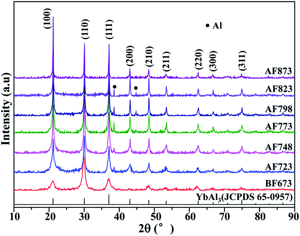 | ||
| Fig. 1 XRD patterns of YbAl3 thin films before and after annealing at different temperatures. | ||
It is very important to examine the crystallinity of the thin films since the preparation of crystalline YbAl3 thin films is a big challenge.23 The XRD patterns were fitted by Rietveld refinement to extract the diffraction intensity of each profile for crystalline YbAl3 and the scattering intensities for amorphous YbAl3. The XC values of YbAl3 thin films before and after annealing treatment were calculated based on the reference intensity ratio method,24
 | (1) |
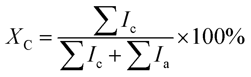
To explain the abnormal decrease of XC for the thin films annealed at high temperatures, the chemical composition along the thickness direction of AF773 thin film was investigated with wavelength-dispersive X-ray spectrometer (WDS) as equipped on the EPMA. The measurements were carried out by changing the acceleration voltages of electron beam (U). Here, WDS instead of energy-dispersive X-ray spectrometer (EDS) was used for quantitative analysis of Yb and Al, because EDS cannot distinguish the small energy difference of the characterized lines between Yb (1.53 keV for Mα line) and Al (1.49 keV for Kα line). In order to gather the composition information along the thickness direction, the excitation depths of electron beam at different U were simulated with the Monte Carlo method suggested by Ritchie.25 As shown in Fig. 2a, the excitation depths of electron beam increase monotonously from 200 nm to 1 μm with increasing the U in the range 8–25 kV. Fig. 2b shows the mole percentages of Al and Yb and Al/Yb atomic ratio of AF773 thin film determined by EPMA at different U. Gradual increase of mole percentage of Yb while reduction of mole percentage of Al and Al/Yb atomic ratio can be found with increasing the U. These results indicate that the content of Al becomes larger and larger while that of Yb becomes smaller and smaller when the detection positions are gradually close to the thin film surfaces. Similar tendency was also found in X-ray photoelectron spectroscopy measurements as given in the ESI (Fig. S1†). The gradient distribution of chemical composition should be attributed to the evaporation of Yb and Al during the annealing process. Since the vapor pressure of Yb (about 5 × 10⁻³ Pa at its melting point 1273 K) is much higher than that of Al (about 2.42 × 10⁻²⁰ Pa at its melting point 933 K),23 the evaporation of Yb should be much easier. Therefore, the abnormal decrease of XC for the thin films annealed at high temperatures should be attributed to the occurrence of decomposition of YbAl3 and the evaporation of Yb and Al.
 | ||
| Fig. 2 (a) Excitation depths of electron beam for EPMA at the different accelerate voltages, U. (b) The mole percentages of Al and Yb and Al/Yb atomic ratio of AF773 thin film at different U. (c) FESEM image and EPMA quantitative analysis to determine the chemical composition of a typical bulge precipitated on the surface of AF773 thin film. The quantitative results are given in the insert. | ||
Composition analysis indicated that the annealing treatment has a large impact on the stoichiometric composition and crystallinity. Increasing the annealing temperature from 723–773 K leads to increased crystallinity and stoichiometric composition, which is favorable for reaching the most equilibrium state of YbAl3. However, a further increase of annealing temperature will drive YbAl3 to nonequilibrium state with loss of Yb and Al, hence leading to lowered crystallinity.
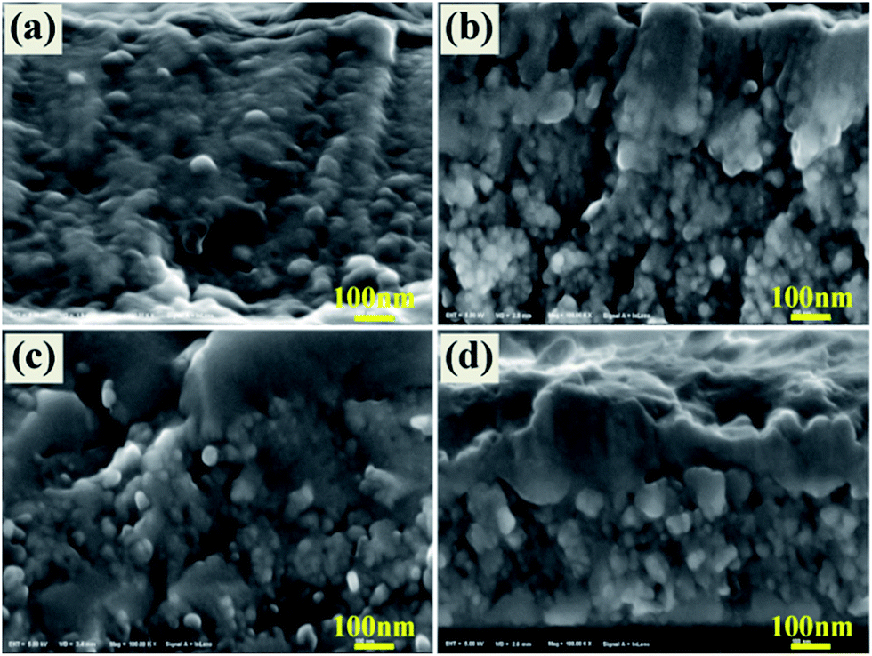
Fig. 3 shows the surface morphology of the as-prepared and the annealed thin films. For the as-prepared thin film (Fig. 3a), sub-μm-sized particles with 0.2–0.5 μm in diameter and μm-sized coarse particles with several μm in diameter can be observed. The enlarged image (Fig. 3b) shows that these sub-μm- and μm-sized particles in fact are aggregated by numerous spherical nanoparticles which have average diameter only ∼30 nm. After annealing, the average size of YbAl3 nanoparticles is enlarged from ∼30 nm to ∼50 nm as shown in Fig. 3c–h. However, the aggregation of nanoparticles and the formation of coarse particles become more significant with increasing the annealing temperature. For the films annealed at high temperatures such as AF773 and AF823, much larger grains can be found due to the abnormal crystallization and growth of YbAl3 particles.
 | ||
| Fig. 3 Surface FESEM images of YbAl3 thin films before and after annealing treatment. (a and b) BF673, (c and d) AF723, (e and f) AF773, and (g and h) AF823. | ||
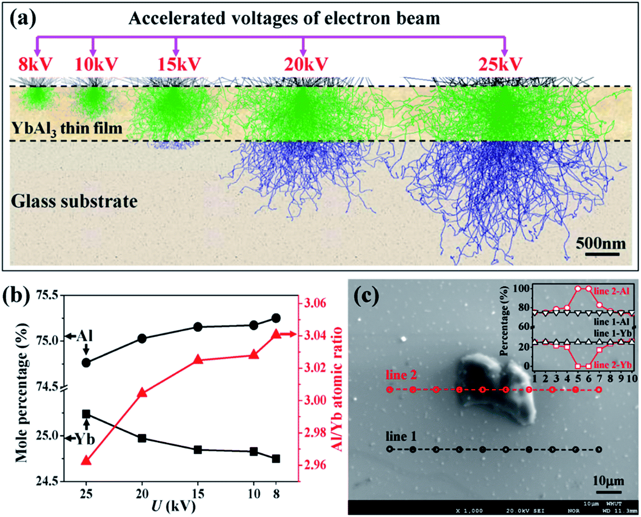
Fig. 4 shows the 3D images of the surface of YbAl3 thin films. Before annealing, the surface of the as-prepared YbAl3 thin film is flat, indicating a uniform sputtering of thin film. After annealing at 723 K, bulges with several μm in diameter and about 1 μm in height distribute randomly on the surface. With increasing the annealing temperature, their sizes including diameter and height gradually increase. The largest bulges have diameter over 10 μm and the height reaches 3 μm after annealing at 823 K.
 | ||
| Fig. 4 3D images of the surface of YbAl3 thin films before and after annealing treatment. (a) BF673, (b) AF723, (c) AF773, and (d) AF823. | ||
In order to clarify the composition of these bulges, EPMA quantitative analysis was performed on the AF773 thin film using a 10 keV acceleration voltage. Fig. 2c shows two individual line scans of WDS with one posed on the flat surface and another crossed a typical bulge. The quantitative results indicate that the composition of the flat surface is YbAl3 with uniform distribution, while the bulge is purely metallic Al. Therefore, the annealing treatment leads to the precipitation of metallic Al on the surface of YbAl3 thin films.
The precipitation and growth of Al bulges on the film surface should influence the surface roughness Ra. The Ra values of the thin films were determined by a stylus method. For the as-prepared YbAl3 thin film, Ra is only 2 nm, implying the uniform sputtering processing due to the small nanoparticles. After annealing, Ra increases to 24 nm for the AF723 thin film and to 54 nm and 115 nm for the AF773 and AF823 thin films, respectively. Since the growth of nanoparticles is not significant with increasing the annealing temperature in the range 723–823 K, the enlarged Ra should be caused by the aggregation of YbAl3 nanoparticles and the growth of Al bulges. The increased content of Al is consistent with the result detected by XRD. Note that the amount of bulges keeps nearly unchanged at different annealing temperatures, suggesting that the nucleation of the bulges has accomplished even at low annealing temperature. It is indeed highly possible since the melting point of Al nanoparticles can be as low as to 773 K.26 In fact, the easy loss of Yb and Al at high annealing temperatures is also closely related to the nanostructures in the thin films, which trend to lower the melting point and decomposition temperature of YbAl3 and Al nanoparticles with reduced surface energy.
Fig. 5 shows the cross-sectional FESEM images of the thin films. The as-prepared thin film consists of numerous nanoparticles, consistent with that observed on the surface. Some amorphous particles are embedded in the thin film, which should be responsible for the low crystallinity (about 42%) as determined by XRD. For the annealed thin films, the less amorphous nanoparticles indicate the increased crystallinity, which is also consistent with the XRD analysis. For the AF773 and AF823 thin films, large grains can be observed on the top of thin film, which should result from the abnormal crystallization of YbAl3 nanoparticles. The abnormal crystallization should be related to the precipitation of Al on the surface. Due to the evaporation of Yb and the precipitation of Al, pores can be found inside the thin films.
 | ||
| Fig. 5 Cross-sectional FESEM images of YbAl3 thin films before and after annealing treatment. (a) BF673, (b) AF723, (c) AF773, and (d) AF823. | ||
The EPMA compositions of YbAl3 thin films determined by WDS are listed in Table 1. The measurements were performed using a 15 keV acceleration voltage and on flat surfaces, in order to determine the average composition of YbAl3 and avoid detecting the Al bulges. The Al/Yb atomic ratio of BF673 thin film was determined to be 3.75, showing a large deviation from the stoichiometric ratio of YbAl3. The excessive Al in the as-prepared film should be in amorphous phase since no characterized peak of Al was detected from the XRD patterns. Therefore, the amorphous particles observed in Fig. 5a should be a mixture of YbAl3 and Al. After annealing, the Al/Yb atomic ratio significantly decreases into a narrow region spanning from 3.03 to 2.98 when the annealing temperature is in the range 773–798 K, indicating the formation of stoichiometric thin films. Therefore, both crystallinity and stoichiometry have been improved after annealing treatment. The decreased content of Al in YbAl3 with increasing the annealing temperature should be caused by the precipitation of Al on the surface, which inevitably leads to increased Al deficiency.
The distribution of Seebeck coefficient on the surface was characterized to reveal the effect of Al precipitation on the transport properties of YbAl3 thin films. Fig. 6a shows the backscattered electron image of the surface of AF773 thin film. The black spots on the surface are metallic Al bulges. Fig. 6b displays the Seebeck coefficient distribution in the same area where 70 × 70 measurement points are included. The α values in the flat area fall in the range from −47 to −56 μV K−1 with an average value of around −52 μV K−1, which are mainly contributed from YbAl3. The distribution is uniform when considering the measuring uncertainty is around ±10%. Around the bulges, the α values are 10–20 μV K−1 lower than those of the flat region. This is predictable since metallic Al possesses much lower Seebeck coefficient than YbAl3 does.27 In addition, some individual points showed large deviations from the average value, which are artifacts originated from the bad contact between the probe and the thin film as caused by the film defects such as pores.
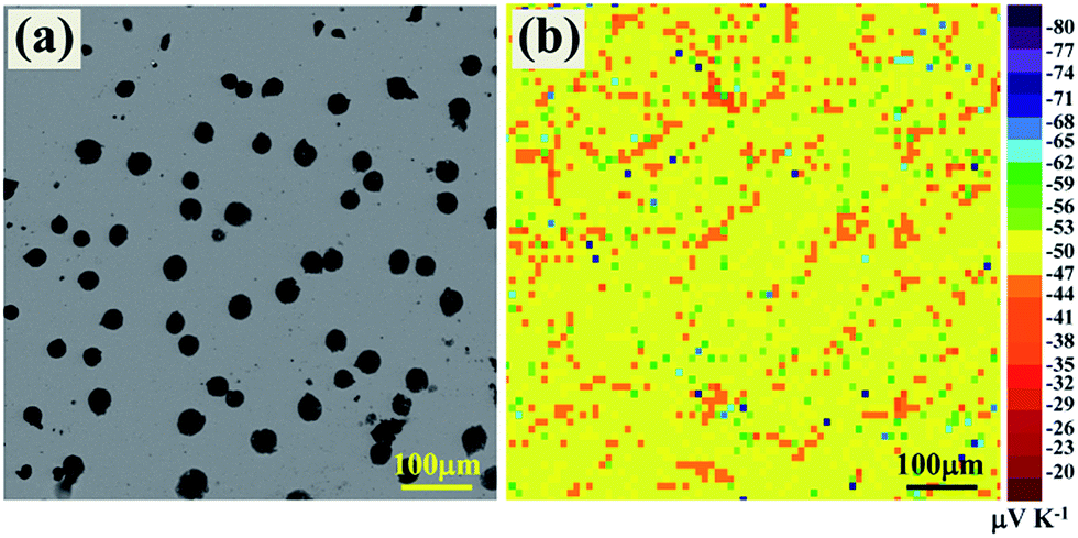 | ||
| Fig. 6 (a) Backscattered electron image of the surface of AF773 thin film and (b) the distribution of Seebeck coefficient in the same area. | ||
The room-temperature transport properties of YbAl3 thin films are listed in Table 1. The carrier concentration n increases with increasing the annealing temperature. The raise in n should be related to the variation of stoichiometric composition. The Al/Yb atomic ratio of thin films decreases from 3.75 to 2.90, which means the increased Al vacancies due to Al precipitation on the film surface.28 Hall mobility μH decreases with the annealing temperature, varied in an opposite trend to n. The decreased μH should originate from the enhanced carrier scattering from electron–electron interactions, structural defects such as pores, and large surface roughness.29 The μH values of YbAl3 thin films are lower than that of the bulk materials,19 which is probably due to the existence of nanostructures and rough surfaces.
The temperature dependences of σ, α, and α2σ for the YbAl3 thin films before and after annealing treatment are shown in Fig. 7. The thin films have very high σ values, which are caused by the high n because of the extremely high density of states near the Fermi level derived from the Yb 4f electrons. σ decreases with increasing the measuring temperature in the range of 300–440 K, indicative of the metallic transport behavior. The reduction in σ originates from the enhanced carrier scattering from lattice at elevated temperatures. The room-temperature σ increases from 1.06 × 10⁶ S m−1 for the BF673 thin film to 1.69 × 10⁶ S m−1 for the AF773 thin film, and then decreases slightly as the annealing temperature is further increased. The increase in σ after annealing treatment is closely relevant to the increased n while the decrease in σ at higher annealing temperatures is a response to the reduced μH.
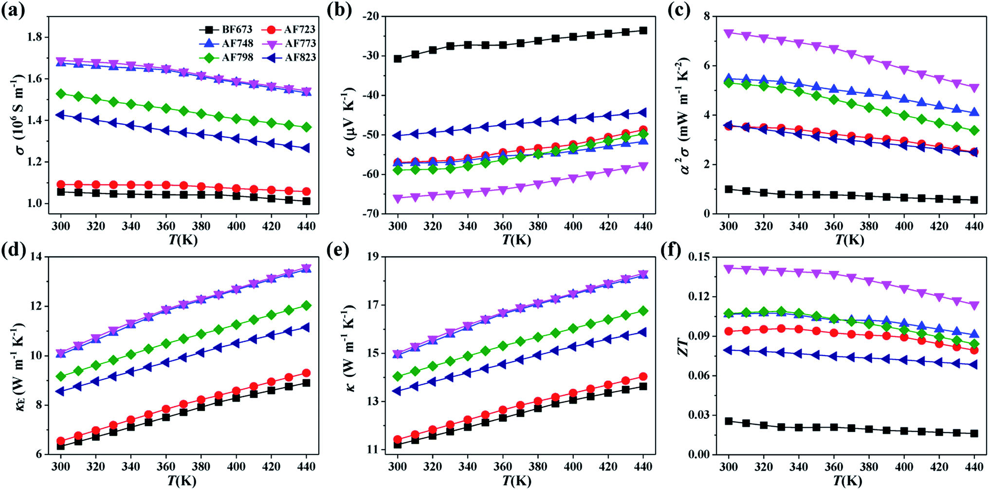 | ||
| Fig. 7 Temperature dependences of (a) electrical conductivity, (b) Seebeck coefficient, (c) power factor, (d) electronic thermal conductivity, (e) estimated thermal conductivity, and (f) estimated ZT for YbAl3 thin films. | ||
The absolute α is only 30.8 μV K−1 before annealing and substantially improved with increasing the annealing temperature in the range of 723–773 K, which is closely related to the significantly improved crystallinity and stoichiometry. At higher annealing temperatures, the absolute α starts to decrease, which should be relevant to the increased n, increased concentration of defects, and reduced crystallinity.30 The highest absolute α reaches 66.0 μV K−1 for the AF773 thin film, which is slightly lower than the value of the highly crystalline YbAl3 bulk materials (about 80.0 μV K−1).18 Higher absolute α is achievable if the crystallinity of thin films could be improved further. Accordingly, the α2σ value is significantly improved at first with increasing the annealing temperature in the range 723–773 K and then decreases above 773 K. The maximum α2σ is 7.4 mW m−1 K−2 for the AF773 thin film, which is much higher than the reported values of other promising TE thin films.30–34 Benefiting from the high electrical conductivity and large power factor, it's expected that the miniaturized TE devices made by YbAl3 thin films have potentially large cooling capacity, large output power, and small Joule heat.
Note that the temperature dependence of electrical conductivity for AF723, AF748, and AF773 thin films shows a bump around 360 K. The decrease of electrical conductivity with temperature becomes more rapid above 360 K. Accordingly, the temperature dependence of Seebeck coefficient also shows abnormal change around 360 K. All these features might be an indication that the Kondo temperature of the annealed YbAl3 thin films is around 360 ± 30 K. The Kondo temperature of 400 K has been reported on a bulk YbAl3 sample.35
Unlike the most of semiconducting TE materials in which the contribution of κ is mainly from the lattice component, in YbAl3 the electronic component contributes largely to the total κ owing to its extraordinarily high σ.18 Therefore, it is possible to estimate κ of YbAl3 thin films using the calculated κE and an averagely high κL obtained on the bulk materials. Fig. 7d and e shows the calculated κE and estimated κ for YbAl3 thin films. Here, κE was calculated from σ according to Wiedemann–Franz law. The reported κL values (e.g. 4.9 W m−1 K−1 at 300 K) of a typical bulk material were incorporated to estimate κ.22 The κ values are over 10 W m−1 K−1 with a large contribution from electrons. Therefore, consideration should be taken in designing TE devices since a large κ is not favorable for building large temperature difference.12 The ZT values can be estimated from α2σ and κ, and the results are given in Fig. 7f. The thin film annealed at 773 K exhibits the highest ZT of 0.14 at 300 K, which is much higher than that of the thin film without annealing treatment (only 0.03) and is comparable with the values of YbAl3 bulk materials (from 0.17 to 0.24).18,19 The significant enhancement in TE properties should be attributed to the largely improved α2σ due to the significantly improved crystallinity and stoichiometry. In fact, the ZT values of YbAl3 thin films must be underestimated since the κL values of YbAl3 thin film should be lower than those of the bulk materials due to additional phonon scattering from nanostructures, amorphous phases, and rough surfaces.
Conclusions
Intermetallic YbAl3 thermoelectric thin films have been prepared using a co-sputtering technique and a subsequent annealing treatment. The as-prepared thin films had low crystallinity and contained nanoparticles with 30 nm in diameter. After annealing treatment, the crystallization and aggregation of YbAl3 nanoparticles led to significantly improved crystallinity. The precipitation of metallic Al on the surface was favorable for attaining stoichiometric YbAl3 thin films. The electrical conductivity and Seebeck coefficient were improved simultaneously at optimized annealing temperature 773 K, which gave rise to a maximum power factor of 7.4 mW m−1 K−2. The largest ZT of the annealed YbAl3 thin film was estimated to be comparable with those of the bulk materials.Acknowledgements
This work was supported by the National Basic Research Program of China (973-program) No. 2013CB632505, National Natural Science Foundation of China (Nos. 11274248, 51521001, 51572210, and 51502228). The technical assistance from the analytical and testing center of Wuhan University of Technology is gratefully acknowledged.References
- G. Slack, in CRC Handbook of Thermoelectrics, ed. D. M. Rowe, CRC Press, Boca Raton, FL, 1995 Search PubMed.
- X. L. Su, P. Wei, H. Li, W. Liu, Y. G. Yan, P. Li, C. Q. Su, C. J. Xie, W. Y. Zhao, P. C. Zhai, Q. J. Zhang, X. F. Tang and C. Uher, Adv. Mater., 2017 DOI:10.1002/adma.201602013.
- G. J. Snyder and E. S. Toberer, Nat. Mater., 2008, 7, 105–114 CrossRef CAS PubMed.
- X. F. Tang, W. J. Xie, H. Li, W. Y. Zhao, Q. J. Zhang and M. Niino, Appl. Phys. Lett., 2007, 90, 012102 CrossRef.
- M. Saleemi, M. S. Toprak, S. H. Li, M. Johnsson and M. Muhammed, J. Mater. Chem., 2012, 22, 725–730 RSC.
- X. Shi, J. Yang, J. R. Salvador, M. F. Chi, J. Y. Cho, H. Wang, S. Q. Bai, J. H. Yang, W. Q. Zhang and L. D. Chen, J. Am. Chem. Soc., 2011, 133, 7837–7846 CrossRef CAS PubMed.
- C. G. Fu, S. Q. Bai, Y. T. Liu, Y. S. Tang, L. D. Chen, X. B. Zhao and T. J. Zhu, Nat. Commun., 2015, 6, 8144 CrossRef PubMed.
- J. P. Heremans, V. Jovovic, E. S. Toberer, A. Saramat, K. Kurosaki, A. Charoenphakdee, S. Yamanaka and G. J. Snyder, Science, 2008, 321, 554–557 CrossRef CAS PubMed.
- L. D. Zhao, H. J. Wu, S. Q. Hao, C. I. Wu, X. Y. Zhou, K. Biswas, J. Q. He, T. P. Hogan, C. Uher, C. Wolverton, V. P. Dravid and M. G. Kanatzidis, Energy Environ. Sci., 2013, 6, 3346–3355 CAS.
- J. B. Zhao, Z. X. Liu, J. Reid, K. Takarabe, T. Iida, B. Wang, U. Yoshiya and J. S. Tse, J. Mater. Chem. A, 2015, 3, 19774–19782 CAS.
- Z. L. Du, T. J. Zhu, Y. Chen, J. He, H. L. Gao, G. Y. Jiang, T. M. Tritt and X. B. Zhao, J. Mater. Chem., 2012, 22, 6838–6844 RSC.
- T. Huesgen, P. Woias and N. Kockmann, Sens. Actuators, A, 2008, 145–146, 423–429 CrossRef CAS.
- J. H. Bahk, H. Y. Fang, K. Yazawa and A. Shakouri, J. Mater. Chem. C, 2015, 3, 10362–10374 RSC.
- R. Venkatasubramanian, E. Siivola, T. Colpitts and B. O'Quinn, Nature, 2001, 413, 597–602 CrossRef CAS PubMed.
- K. J. Shin and T. S. Oh, J. Electron. Mater., 2015, 44, 2026–2033 CrossRef CAS.
- W. Seifert and V. Pluschke, Phys. Status Solidi B, 2014, 251, 1416–1425 CrossRef CAS.
- Q. H. Zhang, X. Y. Huang, S. Q. Bai, X. Shi, C. Uher and L. D. Chen, Adv. Energy Mater., 2015, 18, 194–213 CrossRef.
- D. Q. He, W. Y. Zhao, X. Mu, H. Y. Zhou and Q. J. Zhang, J. Electron. Mater., 2015, 44, 1919–1925 CrossRef CAS.
- J. Q. Li, X. Y. Liu, Y. Li, S. H. Song, F. S. Liu and W. Q. Ao, J. Alloys Compd., 2014, 600, 8–12 CrossRef CAS.
- T. He, T. G. Calvarese, J. Z. Chen, H. D. Rosenfeld, R. J. Small, J. J. Krajewski and M. A. Subramanian, 24th International Conference on Thermoelectrics, 2005, pp. 434–439 Search PubMed.
- A. D. Christianson, V. R. Fanelli, J. M. Lawrence, E. A. Goremychkin, R. Osborn, E. D. Bauer, J. L. Sarrao, J. D. Thompson, C. D. Frost and J. L. Zarestky, Phys. Rev. Lett., 2006, 96, 117206 CrossRef CAS PubMed.
- G. J. Lehr and D. T. Morelli, J. Electron. Mater., 2013, 42, 1697–1701 CrossRef CAS.
- H. Miyazaki, Vacuum, 2008, 83, 416–418 CrossRef CAS.
- B. B. He, Two-dimensional X-ray diffraction, John Wiley & Sons, Hoboken, 2009 Search PubMed.
- N. W. Ritchie, Microsc. Microanal., 2009, 15, 454–468 CrossRef CAS PubMed.
- S. L. Lai, J. R. A. Carlsson and L. H. Allen, Appl. Phys. Lett., 1998, 72, 1098–1100 CrossRef CAS.
- S. Kasap, Thermoelectric Effects in Metals: Thermocouples, An e-Booklet, 2001 Search PubMed.
- J. Zhou, B. S. Sa and Z. M. Sun, Intermetallics, 2010, 18, 2394–2398 CrossRef CAS.
- D. Huang, F. Yun, M. A. Reshchikov, D. Wang, H. Morkoc, D. L. Rode, L. A. Farina, C. Kurdak, K. T. Tsen, S. S. Park and K. Y. Lee, Solid-State Electron., 2001, 45, 711–715 CrossRef CAS.
- T. C. Harman, M. P. Walsh, B. E. Laforge and G. W. Turner, J. Electron. Mater., 2005, 34, 19–22 CrossRef.
- S. R. Sarath Kumar, A. Alyamani, J. W. Graff, T. M. Tritt and H. N. Alshareef, J. Mater. Res., 2011, 26, 1836–1841 CrossRef.
- C. Schumacher, K. G. Reinsberg, R. Rostek, L. Akinsinde, S. Baessler, S. Zastrow, G. Rampelberg, P. Woias, C. Detavernier, J. A. C. Broekaert, J. Bachmann and K. Nielsch, Adv. Energy Mater., 2013, 3, 95–104 CrossRef CAS.
- H. C. Chang, T. H. Chen, W. T. Whang and C. H. Chen, J. Mater. Chem. A, 2015, 3, 10459–10465 CAS.
- X. Mu, H. Y. Zhou, D. Q. He, W. Y. Zhao, P. Wei, W. T. Zhu, X. L. Nie, H. J. Liu and Q. J. Zhang, Nano Energy, 2017, 33, 55–64 CrossRef CAS.
- L. H. Tjeng, S.-J. Oh, E.-J. Cho, H.-J. Lin, C. T. Chen, G.-H. Gweon, J.-H. Park, J. W. Allen, T. Suzuki, M. S. Makivic and D. L. Cox, Phys. Rev. Lett., 1993, 71, 1419–1422 CrossRef CAS PubMed.
Footnote |
| † Electronic supplementary information (ESI) available. See DOI: 10.1039/c7ra02366a |
| This journal is © The Royal Society of Chemistry 2017 |