
 Open Access Article
 This Open Access Article is licensed under a Creative Commons Attribution-Non Commercial 3.0 Unported Licence
Highly sensitive pressure switch sensors and enhanced near ultraviolet photodetectors based on 3D hybrid film of graphene sheets decorated with silver nanoparticles†
Guang Yao a,
Hulin Zhanga,
Shangjie Zhanga,
Feiyi Liaoa,
Zhenlong Huanga,
Bixiong Biebc and
Yuan Lin*a
a,
Hulin Zhanga,
Shangjie Zhanga,
Feiyi Liaoa,
Zhenlong Huanga,
Bixiong Biebc and
Yuan Lin*a
aState Key Laboratory of Electronic Thin Films and Integrated Devices, University of Electronic Science and Technology of China, Chengdu, Sichuan 610054, P. R. China. E-mail: linyuan@uestc.edu.cn
bThe Peac Institute of Multiscale Sciences, Chengdu, Sichuan 610207, P. R. China
cSchool of Science, Wuhan University of Technology, Wuhan, Hubei 430070, P. R. China
First published on 23rd May 2017
Abstract
Pressure switch sensors and near ultraviolet (NUV) photodetectors based on graphene nanosheets and silver nanoparticles composites were proposed and fabricated. X-ray diffraction (XRD), X-ray photoelectron spectroscopy (XPS), Raman spectra, ultraviolet-visible spectroscopy (UV-vis), Fourier transform infrared (FTIR) spectra, energy dispersive spectroscopy (EDS), field effect scanning electron microscopy (FESEM), and transmission electron microscopy (TEM) have been employed to characterize the composites. The device based on a flexible pyramid-structured polydimethylsiloxane (PDMS) substrate was investigated as a pressure sensor, showing that the interface contact resistance can be changed sensitively by the applied pressure. In addition, benefiting from a combined effect of three-dimensional structure and enhanced light absorption of silver nanoparticles, NUV photodetectors based on the composites show a high photocurrent, a short response and recovery time of 2 ms under 365 nm NUV illumination of 0.5 mW cm−2. This work presented a simple route to obtain high performance pressure switch sensors and ultraviolet photodetectors, and would be of some benefit in device manufacture.
1. Introduction
Graphene, a two-dimensional (2D) honeycomb lattice of sp2-hybridized carbon nanomaterial, has been widely studied in the field of materials due to its excellent physical and chemical properties.1–5 This 2D material has a high aspect ratio, which provides a sufficient functional surface and can act as building blocks for nanoparticle intercalation to fabricate graphene-derived materials.6,7 Recently, composites of graphene or graphene oxides (GOs) modified by certain functional materials have played an increasingly important role because the decorated materials can improve their performance for potential applications. More generally, due to various new properties, the metal/graphene hybrid films can be widely used in catalysis, chemical sensors, rechargeable batteries, transparent electrodes and so on.7–15 As a result, composites of graphene decorated with metal nanoparticles have attracted much attention. Mechanical exfoliation of graphite, chemical vapor deposition and chemical and thermal reduction of GOs in colloidal suspensions are three main methods to obtain graphene.1,16,17 The third approach is scalable and versatile to obtain graphene for chemical functionalization and heterogeneous integration. However, chemical reduction can remove the oxygen-containing groups of the insulating GOs to form electrical sp2-hybridized graphene nanosheets (GNs), which also leads to a smaller interlayer distance and provides more chances for GNs restacking and aggregation. Silver with good conductivity and chemical stability is considered as one of the most attractive metal materials. Moreover, when GNs are decorated with Ag NPs, the Ag NPs act as a critical spacer and conductor to prevent aggregation of GNs and increase the electrical conductivity.7,18–21 In addition, because of the efficient localized surface plasmon resonance (LSPR) effect of Ag NPs, surface modification of semiconductive nano-materials by Ag NPs has been endeavored to improve the sensitivity, response and recovery time of functional devices.22–26 The structure and the electrical transport properties of Ag/graphene composites have been extensively explored. However, there are few reports on the devices constructed based on the Ag/GNs 3-dimensional (3D) multi-layered structure.Herein, a solution-based synthesis approach of Ag/GNs composites has been studied. In the synthesis process, GNs were fabricated by the reduction of GO and utilized as the crystal nucleus for Ag NPs decoration. Monodispersed Ag NPs have been successfully inserted into multi-layered GNs to form 3D Ag/GNs composites. Then the composites were spin coated on the flexible polydimethylsiloxane (PDMS) substrates to obtain a sandwich structured pressure switch sensor. To ensure the stability of the device, a pyramid structured PDMS substrate was adhered to the pressure sensor device to disperse the external pressure. Test results show that the interface contact resistance can be changed sensitively by the applied pressure. Additionally, the near ultraviolet (NUV) photodetector was fabricated by loading the composite on N-type Si, which showed obvious enhancements in photoelectric performance to NUV light. The results confirm that the photodetector exhibited good reproducibility and high sensitivity to the NUV light. Correlations between the pressure and resistance of the switch sensor and response to the NUV light of the photodetector were carefully investigated and simple models for the working principle of the sensors have been well established.
2. Experimental
2.1 Materials
Graphene oxide (detailed sample information are shown in Table S1†) and hydrazine hydrate (purity >98 wt%) were purchased from Nanjing XFNANO Materials Tech Co., Ltd. AgNO3 and sodium citrate were obtained from Aladdin Supplies. Potassium hydroxide, ethanol and acetone were purchased from Chengdu Kelong Chemical Reagent Company. Isopropyl alcohol and BOE (HF![[thin space (1/6-em)]](https://www.rsc.org/images/entities/char_2009.gif) :NH4F = 6:1) were acquired from Suzhou Crystal Clear Chemical Co., Ltd. PDMS (silicone elastomer and curing agent) was obtained from Dow Corning Corporation. All the above reagents of analytical grade were utilized as received. Deionized water was used throughout.
:NH4F = 6:1) were acquired from Suzhou Crystal Clear Chemical Co., Ltd. PDMS (silicone elastomer and curing agent) was obtained from Dow Corning Corporation. All the above reagents of analytical grade were utilized as received. Deionized water was used throughout.
2.2 Preparation of GNs and Ag/GNs
A solution-based approach, including sequential reduction of GO and AgNO3, has been carried out to fabricate the Ag/GNs composites. The whole preparation procedure of inserting Ag NPs into GNs is illustrated in Fig. 1.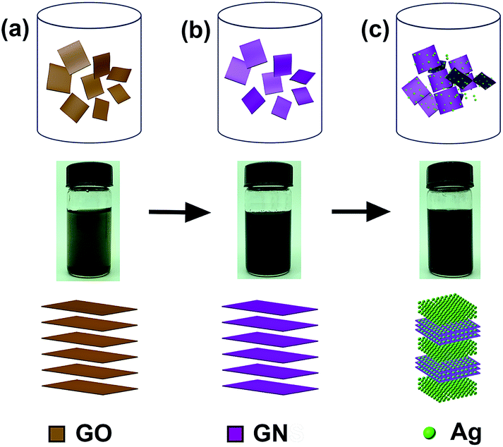 | ||
| Fig. 1 The schematic illustration describing the solution-based chemical approach to obtain Ag/GNs composites, including reduction of graphene oxidation (GO) and AgNO3. (a) GO was uniformly dispersed in deionized water. (b) GNs dispersion by reduction of GO. (c) Modifying the Ag nanoparticles into multi-layered GNs to form a 3D Ag/GNs composites stabilized solution. | ||
Firstly, hydrazine hydrate as a reducing agent was used for GO reduction to obtain conductive graphene sheets with the sp2 network. In a typical synthesis procedure, about 30 mg GO was ultrasonically dispersed in 100 ml deionized water to achieve a homogenous solution without visible particulate matter. Subsequently, 1.0 ml hydrazine hydrate was added into the solution. After heating at 100 °C for 24 h, the mixture turned from yellowish brown to black. The mixture was then cooled to obtain GNs solution for further usage.
To obtain Ag/GNs composites, 45 mg AgNO3 was ultrasonically dispersed in 100 ml deionized water. About 2 mg GNs (7 ml GNs solution) was added to obtain mixed solution. The solution was heated to boiling. Subsequently, 10 ml of 1% sodium citrate was quickly added to the solution. Both the excess hydrazine hydrate and citrate of sodium act as reducing agents, and additionally, citrate of sodium also act as a stabilizing agent.27,28 GNs served as the crystal nucleus for Ag NPs decoration because the reduced graphene is suitable to chemical functionalization and heterogeneous integration. Thus, Ag+ was successfully reduced to be monodispersed nanoparticles, which will be loaded on multi-layered GNs to fabricate a 3D Ag/GNs colloids. After heating at 100 °C for 1 h, the mixture was then cooled, filtered and washed several times with deionized water for further usage. The solution was stabilized by electrostatic repulsion, and it has no layering for a long time (the photographs in different periods were shown in Fig. S1†).
2.3 Characterizations
The crystal phase, morphology and microstructure of the samples were characterized using the X-ray diffraction (XRD; Bruker, λ = 1.54056), Raman spectrometer (Renishaw inVia Raman microscope), UV-visible spectrometer (Thermo Scientific Evolution), Fourier-transform infrared spectrometer (FTIR; Nicolet IS50), X-ray photoelectron spectroscopy (XPS; Escalab 250), field emission scanning electron microscopy (FESEM; Hitachi S4800) and a high-resolution transmission electron microscope (HRTEM; Tecnai G2 F20 S-TWIN). Amount of silver present in the Ag/GNs composites materials was estimated by Inductively Coupled Plasma Optical Emission Spectrometer (ICP-OES). The results show that the amount of silver is about 4 wt%. The measurements were conducted under the same environmental conditions, such as temperature, humidity, etc.2.4 Fabrication of pressure sensors and photodetectors
For the pressure switch sensor, the centrifuged Ag/GNs composites was coated onto the PDMS (10:1) substrate and covered with the PDMS (20:1) substrate to form a sandwich structure. Then the pyramid-array-structured PDMS (20:1) was placed on the top of the device (the flowchart schematic of fabricating pyramid-array-structured PDMS substrates were shown in Fig. S2†). The PDMS (20:1) has a better viscoelasticity because it has a smaller Young's modulus and bigger adhesion strength.29,30 Eventually, the whole surface of device was encapsulated by Kapton tape, as shown in Fig. 2. For comparison, a device based on an ordinary PDMS substrate without microstructure was also prepared. As for the NUV photodetector, zirconium dioxide was deposited on N-type Si (covered with a mask) acting as insulating layer by dc-sputtering techniques. Then, the substrate was covered with centrifuged Ag/GNs composites to form a P–N junction. The schematic illustration describing the formation and measurement of NUV photodetector was shown in Fig. 2. A device based on bare GNs was prepared as a reference sample.
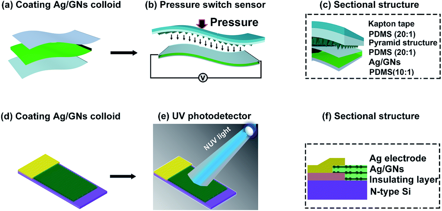 | ||
| Fig. 2 Flowchart schematic illustration describing the formation and measurement of the pressure sensitive sensor on flexible PDMS substrates and the NUV photodetector on N-type Si substrate. | ||
2.5 Pressure response and photo response measurements
For pressure measurement, the magnitude and frequency of the pressure was controlled by a linear stepping motor. For photodetector measurement, light signals (365 nm, 405 nm, 808 nm, visible white light, respectively) with a power density of 0.5 mW cm−2 were controlled by a function generator. Agilent B2901A was employed for the electrical measurements. All the measurements were carried out at room temperature.3. Results and discussion
3.1 Characterizations
The crystallinity and phases of the as-prepared Ag/GNs were examined by XRD. Normal (χ = 0°) XRD θ–2θ scanning patterns were measured from 5.0° to 80.0°. From comparison with the GO and GNs, all the peaks of Ag/GNs in the patterns can be indexed, suggesting that graphene oxidation was successfully reduced and the Ag NPs were well decorated on the GNs, as shown in Fig. 3a. The grain size of Ag NPs can be calculated according to the Scherrer equation, D = Kλ/(βcosθ), where K (0.89) is Scherrer constant, λ (0.15406 nm) is the X-ray wavelength, β (0.923) is the full width at half maximum (FWHM) and θ is the diffraction angle. Based on the above formula, the spherical Ag grain size D (≈9 nm) can be estimated. Based on the Bragg spacing equation 2dsinθ = nλ (d is defined as the interplanar spacing), the layer-to-layer distance of GNs in the Ag/GNs composites is about 0.363 nm, which is larger than that of graphite with layer spacing distance (0.335 nm), suggesting the Ag NPs can maintain the interlayer space and prevent restacking and aggregation of GNs.19,20
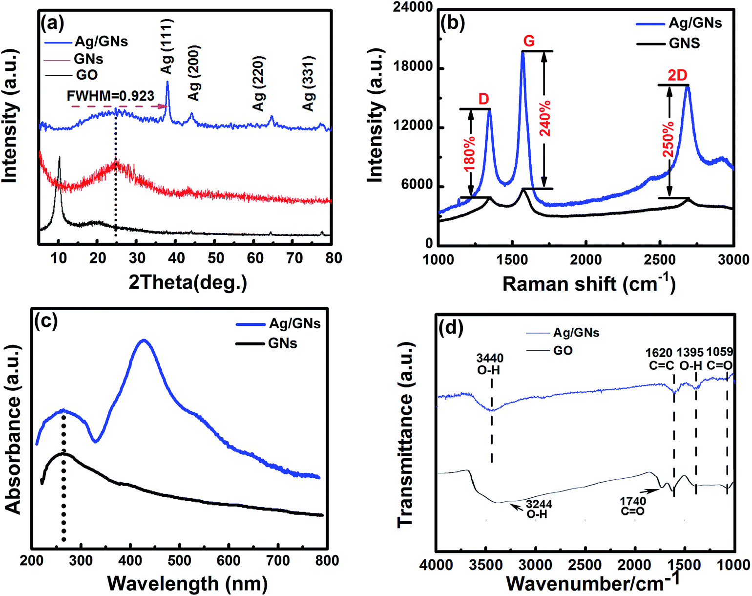 | ||
| Fig. 3 (a) Normal (χ = 0°) XRD θ–2θ scanning patterns for samples. Bottom to top are GO (2θ = 10.22°), GNs (2θ = 24.55°) and Ag/GNs composites (2θ = 38.1°, 44.3°, 64.4°, 77.4° can be assigned to the (111), (200), (220), (331) crystalline planes of Ag). (b) Raman spectra for GNs and Ag/GNs composites, respectively. The Ag NPs enhance the intensity of D, G and 2D bands by 180%, 240% and 250%, respectively. (c) Ultraviolet-visible absorption spectra of GNs and Ag/GNs composites, respectively. (d) FTIR transmittance spectra of GO and Ag/GNs composites, respectively. | ||
Surface enhanced Raman spectroscopy (SERS) on noble metal nanoparticles has been reported,20,31,32 which can be assigned to chemical and electromagnetic enhancements. As shown in Fig. 3b, D, G and 2D bands are observed in Raman spectra of GNs and Ag/GNs composites, and the intensities of these bands for the Ag/GNs hybrid film increased about two- to three folds compared with the bare GNs. Thus, low enhancement factors (180–250%) suggest that the charge-transfer complexes with chemical bond or interaction between Ag NPs and GNs were generated at the contact area.22 The result further confirms that graphene oxide was successfully reduced and the Ag NPs were well inserted into the GNs.
Fig. 3c shows the ultraviolet-visible absorption spectra of aqueous dispersion of GNs and Ag/GNs composites, GNs displays a strong absorption peak centered at 260 nm which corresponds to π/π* transitions of aromatic C–C bonds. Thus, the π electronic conjugation has been restored within the graphene sheets after reduction. After decoration with Ag NPs onto the surface of graphene, ultraviolet-visible spectroscopy absorption spectrum of Ag/GNs shows a new broad peak centered at about 420 nm corresponding to localized surface plasmon resonance (LSPR) peak of Ag NPs, which further implies the formation of Ag NPs on GNs.
FTIR transmittance spectroscopy was used to evaluate the degree of reduction of GO. The FTIR spectra of GO and Ag/GNs composites are shown in Fig. 3d. For GO, the broad peak centred at 3244 cm−1 is attributed to the O–H stretching vibrations, whereas the peaks at 1740, 1620 and 1059 cm−1 are assigned to the C![[double bond, length as m-dash]](https://www.rsc.org/images/entities/char_e001.gif) O stretching, sp2-hybridized CC group and C–O vibration of the epoxy or alkoxy groups, respectively.33–35 For Ag/GNs composites, after the GO is chemically reduced, the CO vibration band (carboxylic acid and carbonyl moieties at ∼1740 cm−1) disappears, the O–H and the C–O stretching bands remain, while the broad peak centered at 3440 cm−1 could be due to the O–H stretching mode of intercalated water.33,34 In addition, Fig. 3d shows that the peak intensities of the oxygen-containing groups decrease significantly, which indicates the effective removal of oxygen-containing groups.
O stretching, sp2-hybridized CC group and C–O vibration of the epoxy or alkoxy groups, respectively.33–35 For Ag/GNs composites, after the GO is chemically reduced, the CO vibration band (carboxylic acid and carbonyl moieties at ∼1740 cm−1) disappears, the O–H and the C–O stretching bands remain, while the broad peak centered at 3440 cm−1 could be due to the O–H stretching mode of intercalated water.33,34 In addition, Fig. 3d shows that the peak intensities of the oxygen-containing groups decrease significantly, which indicates the effective removal of oxygen-containing groups.
The XPS analysis was performed to further investigate the chemical compositions of as-prepared composites. Fig. 4a presents the typical XPS survey spectra in the binding energy range of 0 to 1000 eV of GO and Ag/GNs composites. GO spectra shows only C and O XPS peaks, while Ag/GNs spectra show the signals of Ag 3d, Ag 3p1, and Ag 3p5.36 The high-resolution XPS spectra of Ag/GNs for C 1s, Ag 3d peak doublets and O 1s peak are shown in Fig. 4b, c and d, respectively. The high-resolution C 1s spectra (Fig. 4b) illustrate that the intensities of all oxygen-containing bonds (CO, C–O and C–OH) decline dramatically after the chemical reduction, which indicates the considerable de-oxygenation by the reduction process.34,35,37 As shown in Fig. 4c, relevant high-resolution Ag 3d XPS spectra contain two peaks at 368.4 eV and 374.4 eV, corresponding to Ag 3d5/2 and Ag 3d3/2, respectively.36 In the meantime, the binding energy of the O 1s photoelectron peak is at 530.4 eV (Fig. 4d). XPS analysis has proved again the formation of Ag/GNs composites.
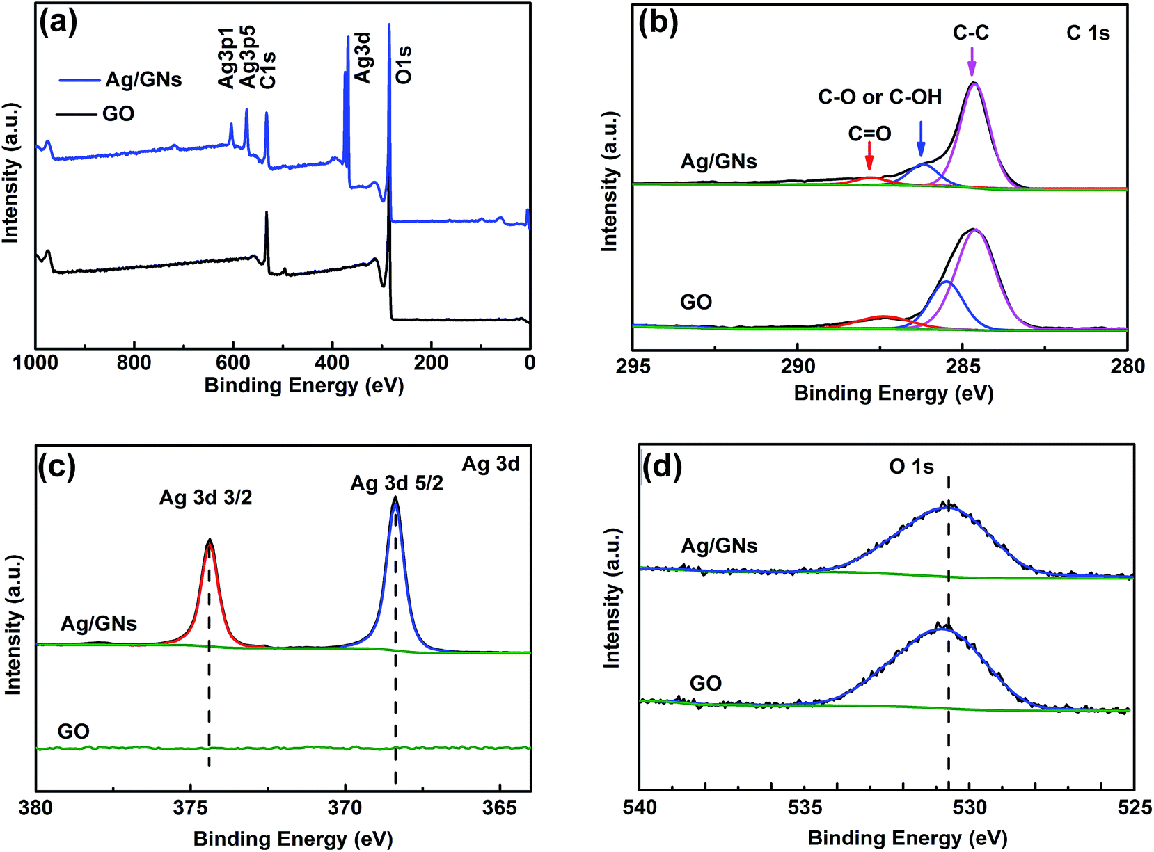 | ||
| Fig. 4 XPS spectra of GO and Ag/GNs composites. (a) Typical survey spectra. (b) C 1s core level. (c) Ag 3d core level. (d) O 1s core level. | ||
FESEM images of GNs and GNs/Ag composites are shown in Fig. 5a, respectively. The energy dispersive spectrometer (EDS) elemental mapping results of Si, C, Ag of the Ag/GNs composites are shown in Fig. 5b and the EDS spot analysis result is shown in Fig. 5c, which confirm the presence of silver and carbon elements without other impurities (Si is from the substrate). TEM was employed to further study how the Ag NPs combined with the GNs, as shown in Fig. 5d–f. Compared with the TEM images of bare GNs and Ag NPs (Fig. 5d), as shown in image for the Ag/GNs composites (Fig. 5e), it can be seen that the Ag NPs are uniformly located on the graphene frames with few Ag agglomerations. The TEM image reveals that the Ag particles are of about 10 nm in average diameter, which is consistent with the result of XRD. The Fig. 5f is the high-resolution TEM image of a single Ag particle attached on the graphene nanosheets, which exhibits clear lattice fringes, indicating high crystallinity of the nanoparticle. Top and side views of structured PDMS are show in shown in Fig. S3.† Pyramidal PDMS (20:1) structure with sidewalls aligned to the mask edge was well produced. Additionally, the top and cross section morphologies of pressure switch sensor were shown in Fig. S4,† and the cross-sectional thickness of the device is about 2 μm. From the results of various characterizations above, we know that the components of as-designed pressure sensor have been obtained successfully.
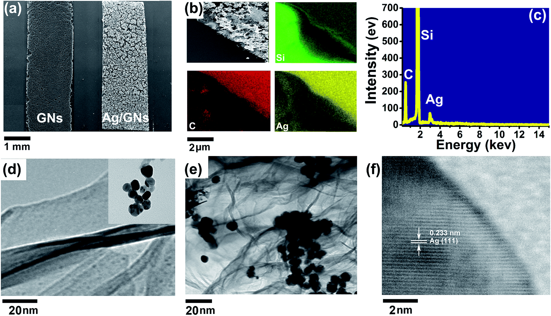 | ||
| Fig. 5 (a) FESEM images of GNs and GNs/Ag composites, respectively. (b) Energy dispersive spectrometer (EDS) maps of Si (green), carbon (red) and Ag (yellow). (c) EDS spot analysis of Ag/GNs composites. (d) TEM images of GNs and Ag NPs (inset). (e) TEM image of Ag/GNs composites. (f) HRTEM image of Ag/GNs. | ||
3.2 Pressure-response of the as-prepared 3D microstructured device
To explore the applications of the as-fabricated pressure switch device, the resistance of the device was measured under different pressures. As shown in Fig. 6a, the device has an original resistance of 3300 Ω, and the stabilized resistance is about 90 Ω at a big enough external pressure, which is reasonable considering the resistivity results of the materials in the previous report (GNs ∼ 8200 Ω m−1, Ag/GNs composites ∼ 93 Ω m−1).19 As is illustrated in Fig. 6b, with the external pressure increasing within a small range, the resistance show a sharply decline. However, when the pressure reaches a certain extent, the resistance is relatively stable. Responses of device under different external pressure with various periods are shown in Fig. 6c, suggesting the device has a high sensitivity and stability. To evaluate the repeatability of the device in practical applications, the resistance response of our constructed device as a pressure switch sensor was recorded in a long period, as is plotted in Fig. 6d. The excellent switching response of the device was clear and stable when the pressure was periodically switched on and off, which further demonstrated that it can be potentially applied in pressure switching or sensing.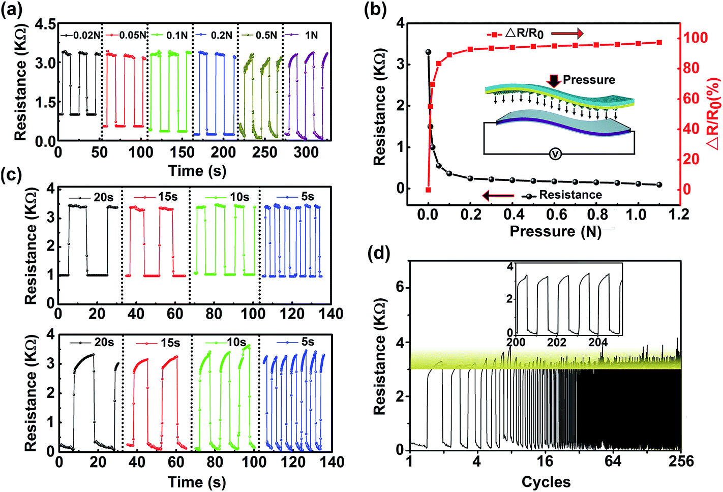 | ||
| Fig. 6 Characterization of the resistance under different pressures. (a) Resistance of the device under different pressures with the period of 20 seconds. (b) The resistance change and relative resistance change versus the applied pressure. (c) The response to external pressure (the top figure is 0.02 N and the bottom figure is 0.5 N) with different periods (5 s, 10 s, 15 s and 20 s). (d) The long-term response of the switch sensor under 1 N for 250 cycles. | ||
The response to pressure can be attributed to the change of the contact resistance. The external pressure will be dispersed and evenly applied on the 3D Ag/GNs composites due to the pyramid structure. The Ag/GNs composites will act as a spring since the Ag NPs is an excellent nanospacer. With the external pressure applied, the alternate-superimposed 3D microstructure will be compressed, which provides more chance for Ag NPs touching with each other, resulting in the decrease of resistance. Conversely, spatial distance and the contact state will recover to the original state when the pressure is removed. However, at a higher pressure, there is a ramp appearing in the stabilized process of the response curve, which can be attributed to compression deformation of the Ag NPs and pyramid structured PDMS and this interesting behavior is explained in detail in Fig. S5.† In addition, a reference device without pyramid-structured PDMS was also prepared for comparison, and the pressure response of reference device with different periods are also shown in the Fig. S5.†
3.3 Photocurrent response of NUV photodetector
NUV photodetectors based on Ag/GNs composites were fabricated to verify the improved sensitivity induced by the combination of 3D structure and LSPR effect of Ag NPs. Fig. 7a shows the working principle of the assembled device. The photocurrent measurements were conducted under illumination of LED light at room temperature. Fig. 7b shows I–V characteristics of the fabricated Ag/GNs photodetector measured in dark and under light illumination with different wavelengths (365 nm, 405 nm, 808 nm and visible white light). The asymmetry in the recorded I–V plots demonstrated the Schottky contact between Ag/GNs composites and N-type Si substrates. As shown in Fig. 7b, the photocurrent responses of Ag/GNs sample are higher than those of GNs sample at the irradiation with wavelengths of 365 nm, 405 nm and white light. However, with the wavelength increasing, the photocurrent response decline gradually, which is consistent with the results of UV-vis absorption spectra of GNs and Ag/GNs composites. When the irradiation wavelength reaches 808 nm, there is no obvious current response difference between GNs and Ag/GNs. Thus, the results reveals localized surface plasmon resonance (LSPR) of Ag nanoparticles in the Ag/GNs composites can be applied to the near ultraviolet region and visible region.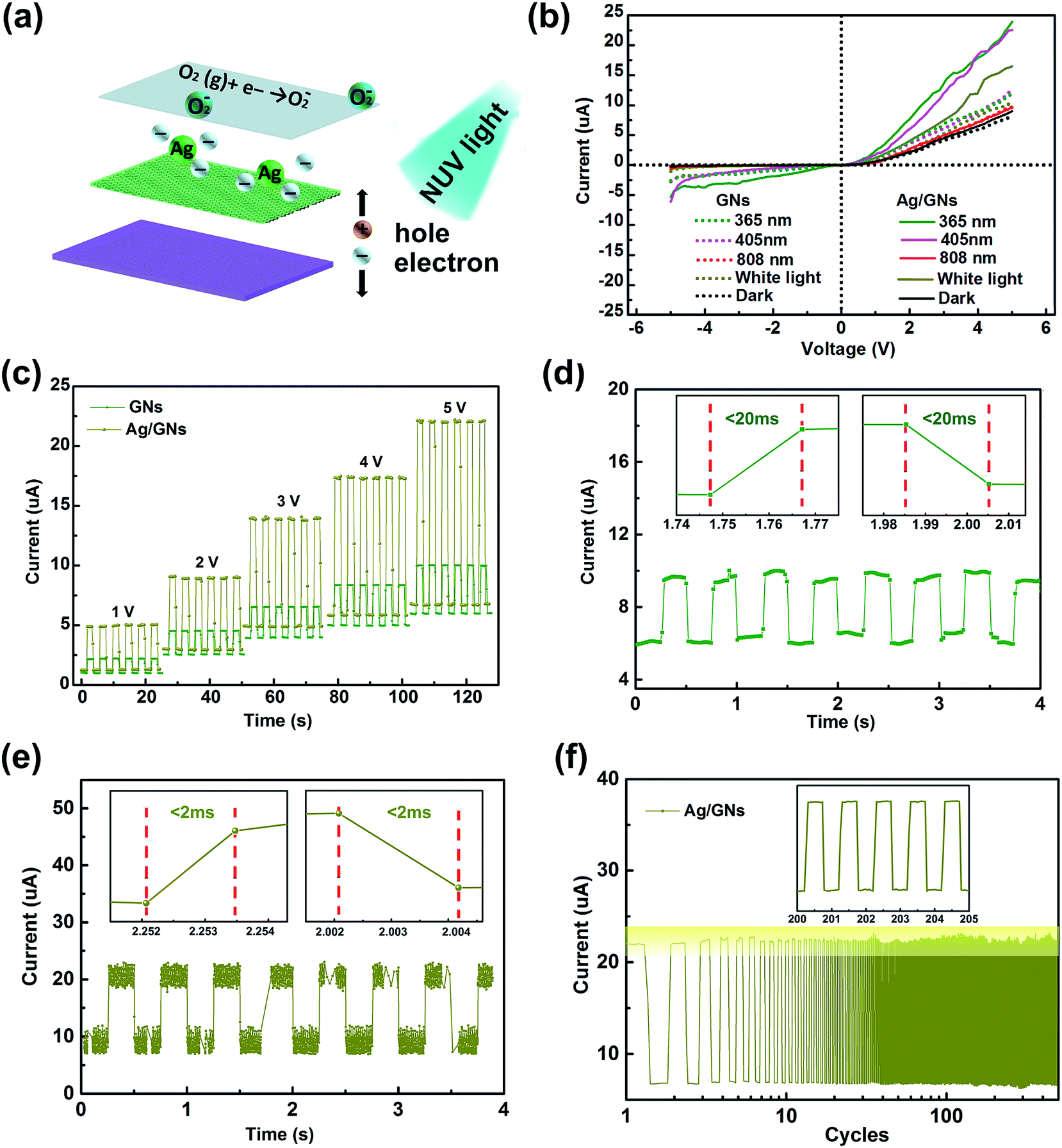 | ||
| Fig. 7 (a) The working principle of the Ag/GNs photodetector. (b) I–V characteristics of the GNs and Ag/GNs photodetectors in dark and under irradiations with various wavelengths (365 nm, 405 nm, 808 nm, visible white light). (c) Photocurrent response under NUV light (365 nm, 0.5 mW cm−2) from 1 V to 5 V bias with NUV light periodically switched on and off. (d) Response and recovery time of GNs photodetectors at 5 V bias. (e) Response and recovery time of Ag/GNs photodetectors at 5 V bias. (f) The long-term (500 cycles) response of Ag/GNs photodetectors at 5 V bias. | ||
In the near ultraviolet region, compared with the pure GNs sample, the Ag NPs coating layer would tremendously improve the photocurrent of the prepared detector. At an applied bias from 1 V to 5 V, the fabricated photodetector could be turned on/off reversibly, by switching the NUV illumination (365 nm) with a period of 4 s (Fig. 7c). All samples were measured by periodic on/off radiation with 50% on–off ratio. Furthermore, to estimate the ultrafast response and recovery from the NUV illumination, photocurrent transient properties of the samples with or without Ag NPs measured under NUV LED on/off shift were shown in Fig. 7d and e, respectively. For pure GNS device, the response and recovery time was 20 ms. After Ag NPs loaded GNs device, the response and recover time was 2 ms. These results indicate that the photodetector decorated with Ag NPs has an enhanced photocurrent and a short response and recovery time.
Generally, owing to the high aspect ratio of GNs, oxygen trapped on the surface plays an important role in photocurrent response. At ambient conditions, oxygen molecules are adsorbed on the GNs surface by capturing free electrons and ionized (O2 (g) + e− → O2−), resulting in a surface depletion layer, as shown in Fig. 7a. After NUV light irradiation, the photogenerated holes can migrate to surface, react with ionized oxygen, and then release free oxygen molecules. Due to the limited amount of ionized oxygen, the surface depletion layer is not sufficient to separate all of photogenerated electron–hole pairs, leading to the recombination of some photogenerated electron–hole pairs at the GNs defect location. As mentioned above, Ag NPs act as a useful spacer to increase the inter-layer distance, which efficiently inhibit restocking and aggregation of GNs and provide a larger space. Thus, Ag NPs can cooperate with the surface depletion layer to separate the electron–hole pairs more efficiently, and result in the remarkable photocurrent increase and short response time, as shown in Fig. 7c–e. On the other hand, the electrons transfer from Ag NPs to GNs by LSPR can increase the photocurrent directly.32,38 The concrete process of the LSPR effect can be expressed as follows: when the wavelength of irradiated UV is larger than the size of Ag NPs, the high-density electrons in Ag NPs would induce an oscillating electron cloud. Furthermore, the electron transfer is very fast because the hot electron was oscillated with illuminated light at a high frequency. Therefore, the performance of the NUV photodetector could be greatly enhanced with the shorter response time by coating the Ag nanoparticles on the surface of the GNs. Moreover, another factor must be evaluated is the repeatability and long-term stability of the ultraviolet photodetector. The typical results for Ag/GNs is shown in Fig. 7f. It is clear that the variation is very small, demonstrating that the sensors have good stability and is reliable for NUV detection.
4. Conclusions
Ag nanoparticles have been successfully attached to the as-prepared graphene nanosheets to form a 3D multi-layered Ag/GNs structure. The pressure switch sensor device based on the Ag/GNs composites and flexible pyramid-structured PDMS substrates shows high sensitivity and excellent long-term stability. The NUV photodetector based on the composites exhibits good reproducibility and high sensitivity to the NUV light. This research presented a simple route to obtain high performance pressure switch sensor and NUV photodetector.Acknowledgements
This work is supported by the National Basic Research Program of China (973 Program) under Grant No. 2015CB351905, the National Natural Science Foundation of China (no. 61504019), the Technology Innovative Research Team of Sichuan Province of China (no. 2015TD0005) and “111” project (no. B13042).References
- K. S. Novoselov, A. K. Geim, S. Morozov, D. Jiang, Y. Zhang, S. A. Dubonos, I. Grigorieva and A. Firsov, Science, 2004, 306, 666–669 CrossRef CAS PubMed.
- A. K. Geim and K. S. Novoselov, Nat. Mater., 2007, 6, 183–191 CrossRef CAS PubMed.
- Y. Zhu, S. Murali, W. Cai, X. Li, J. W. Suk, J. R. Potts and R. S. Ruoff, Adv. Mater., 2010, 22, 3906–3924 CrossRef CAS PubMed.
- F. Schedin, A. Geim, S. Morozov, E. Hill, P. Blake, M. Katsnelson and K. Novoselov, Nat. Mater., 2007, 6, 652–655 CrossRef CAS PubMed.
- J. T. Robinson, F. K. Perkins, E. S. Snow, Z. Wei and P. E. Sheehan, Nano Lett., 2008, 8, 3137–3140 CrossRef CAS PubMed.
- S. Stankovich, D. A. Dikin, G. H. Dommett, K. M. Kohlhaas, E. J. Zimney, E. A. Stach, R. D. Piner, S. T. Nguyen and R. S. Ruoff, Nature, 2006, 442, 282–286 CrossRef CAS PubMed.
- K. Gotoh, T. Kinumoto, E. Fujii, A. Yamamoto, H. Hashimoto, T. Ohkubo, A. Itadani, Y. Kuroda and H. Ishida, Carbon, 2011, 49, 1118–1125 CrossRef CAS.
- M. Liang and L. Zhi, J. Mater. Chem., 2009, 19, 5871–5878 RSC.
- S. Ramaprabhu, J. Mater. Chem., 2012, 22, 18775–18783 RSC.
- W. Chen, R. Rakhi and H. Alshareef, J. Mater. Chem., 2012, 22, 14394–14402 RSC.
- Y. Liu, X. Dong and P. Chen, Chem. Soc. Rev., 2012, 41, 2283–2307 RSC.
- Y. Zhu, Z. Sun, Z. Yan, Z. Jin and J. M. Tour, ACS Nano, 2011, 5, 6472–6479 CrossRef CAS PubMed.
- Y. Chen, Y. Li, M. Yip and N. Tai, Compos. Sci. Technol., 2013, 80, 80–86 CrossRef CAS.
- J.-W. Zha, B. Zhang, R. K. Li and Z.-M. Dang, Compos. Sci. Technol., 2016, 123, 32–38 CrossRef CAS.
- M. Zhang, Y. Zhao, L. Yan, R. Peltier, W. Hui, X. Yao, Y. Cui, X. Chen, H. Sun and Z. Wang, ACS Appl. Mater. Interfaces, 2016, 8, 8834–8840 CAS.
- D. Li, M. B. Mueller, S. Gilje, R. B. Kaner and G. G. Wallace, Nat. Nanotechnol., 2008, 3, 101–105 CrossRef CAS PubMed.
- H. J. Park, J. Meyer, S. Roth and V. Skákalová, Carbon, 2010, 48, 1088–1094 CrossRef CAS.
- X. Zhou, X. Huang, X. Qi, S. Wu, C. Xue, F. Y. Boey, Q. Yan, P. Chen and H. Zhang, J. Phys. Chem. C, 2009, 113, 10842–10846 CAS.
- H.-W. Tien, Y.-L. Huang, S.-Y. Yang, J.-Y. Wang and C.-C. M. Ma, Carbon, 2011, 49, 1550–1560 CrossRef CAS.
- Z. Xu, H. Gao and H. Guoxin, Carbon, 2011, 49, 4731–4738 CrossRef CAS.
- L. Chen, P. Zhao, H. Xie and W. Yu, Compos. Sci. Technol., 2016, 125, 17–21 CrossRef CAS.
- G. A. Baker and D. S. Moore, Anal. Bioanal. Chem., 2005, 382, 1751–1770 CrossRef CAS PubMed.
- G. Giovannetti, P. Khomyakov, G. Brocks, V. Karpan, J. Van den Brink and P. Kelly, Phys. Rev. Lett., 2008, 101, 026803 CrossRef CAS PubMed.
- K. T. Chan, J. Neaton and M. L. Cohen, Phys. Rev. B: Condens. Matter Mater. Phys., 2008, 77, 235430 CrossRef.
- K. Yuan, L. Chen and Y. Chen, ACS Appl. Mater. Interfaces, 2014, 6, 21069–21077 CAS.
- S. Dutta, C. Ray, S. Sarkar, M. Pradhan, Y. Negishi and T. Pal, ACS Appl. Mater. Interfaces, 2013, 5, 8724–8732 CAS.
- M. G. Guzmán, J. Dille and S. Godet, Int. J. Chem. Biomol. Eng., 2009, 2, 104–111 Search PubMed.
- S. Zhang, H. Zhang, G. Yao, F. Liao, M. Gao, Z. Huang, K. Li and Y. Lin, J. Alloys Compd., 2015, 652, 48–54 CrossRef CAS.
- D. Armani, C. Liu and N. Aluru, Micro Electro Mechanical Systems: 1999. MEMS'99. Twelfth IEEE International Conference on, IEEE, 1999, pp. 222–227 Search PubMed.
- K. Khanafer, A. Duprey, M. Schlicht and R. Berguer, Biomed. Microdevices, 2009, 11, 503–508 CrossRef CAS PubMed.
- K. Jasuja and V. Berry, ACS Nano, 2009, 3, 2358–2366 CrossRef CAS PubMed.
- J. Li and C. Y. Liu, Eur. J. Inorg. Chem., 2010, 8, 1244–1248 CrossRef.
- H.-L. Guo, X.-F. Wang, Q.-Y. Qian, F.-B. Wang and X.-H. Xia, ACS Nano, 2009, 3, 2653–2659 CrossRef CAS PubMed.
- A. M. Golsheikh, N. M. Huang, H. N. Lim and R. Zakaria, RSC Adv., 2014, 4, 36401–36411 RSC.
- L. Zheng, G. Zhang, M. Zhang, S. Guo and Z. H. Liu, J. Power Sources, 2012, 201, 376–381 CrossRef CAS.
- Z. Fan, B. Liu, J. Wang, S. Zhang, Q. Lin, P. Gong, L. Ma and S. Yang, Adv. Funct. Mater., 2014, 24, 3933–3943 CrossRef CAS.
- Y. Zhou, J. Yang, X. Cheng, N. Zhao, H. Sun and D. Li, RSC Adv., 2012, 3, 3391–3398 RSC.
- Y. Liu, X. Zhang, J. Su, H. Li, Q. Zhang and Y. Gao, Opt. Express, 2014, 22, 30148–30155 CrossRef CAS PubMed.
Footnote |
| † Electronic supplementary information (ESI) available. See DOI: 10.1039/c7ra02342a |
| This journal is © The Royal Society of Chemistry 2017 |