
 Open Access Article
 This Open Access Article is licensed under a Creative Commons Attribution-Non Commercial 3.0 Unported Licence
Bose–Einstein oscillators and the excitation mechanism of free excitons in 2D layered organic–inorganic perovskites
Bo Peng *a,
Jian Lia,
Qi Lia,
Yue Lia,
Hai Zhub,
Li Zhanga,
Xin Wanga,
Lei Bia,
Haipeng Lua,
Jianliang Xiea,
Longjiang Deng*a,
Qinghua Xu*b and
Kianping Loh*b
*a,
Jian Lia,
Qi Lia,
Yue Lia,
Hai Zhub,
Li Zhanga,
Xin Wanga,
Lei Bia,
Haipeng Lua,
Jianliang Xiea,
Longjiang Deng*a,
Qinghua Xu*b and
Kianping Loh*b
aNational Engineering Research Centre of Electromagnetic Radiation Control Materials, State Key Laboratory of Electronic Thin Films and Integrated Devices, School of Microelectronics and Solid State Electronics, University of Electronic Science and Technology of China, Chengdu 610054, China. E-mail: bo_peng@uestc.edu.cn; denglj@uestc.edu.cn
bDepartment of Chemistry, Centre for Advanced 2D Materials and Graphene Research Centre, National University of Singapore, 3 Science Drive 3, Singapore 117543. E-mail: chmxqh@nus.edu.sg; chmlohkp@nus.edu.sg
First published on 27th March 2017
Abstract
Following intense research on two-dimensional (2D) materials, there has been a resurgence of interest in 2D layered hybrid organic–inorganic perovskites. These 2D perovskites have direct band gaps regardless of their thickness. Excitons are confined to monolayers because of the materials' self-organized quantum-well electronic structure. Gaining insight into the exciton dynamics is central to understanding the light–matter interactions in 2D organic–inorganic perovskites. Herein, we investigate the free-exciton dynamics in 2D layered CH3(CH2)3NH3PbI4 perovskite, demonstrating an anomalous temperature variation of the photoluminescence (PL) energy, which deviates from the conventional Varshni formula and is consistent with the behaviour of Bose–Einstein oscillators. The acoustic phonons induced by the coherent lattice motion of the atoms result in a positive temperature variation. Two-pulse emission modulation measurements reveal the excitation mechanism of the strong two-photon PL in CH3(CH2)3NH3PbI4 perovskite, in which two photons are simultaneously absorbed through a virtual state.
Introduction
Hybrid organic–inorganic CH3NH3PbX3 (X = I, Br, Cl) perovskites exhibit strong solar absorption, long electron–hole diffusion lengths and low trap densities.1 Thus, they show fascinating prospects for use in high-efficiency, low-cost solar cells.2–10 The efficiencies of such solar cells exceed 20%.11–13 All-inorganic halide perovskites (CsPbX3) synthesized in the form of colloidal quantum dots have also attracted intense interest because of their high quantum yields of up to 90%.14–17 To investigate the occurrence of two-dimensionally confined properties, ultra-thin CH3NH3PbX3 perovskite single-crystal flakes have been prepared through mechanical exfoliation,18 chemical vapour deposition (CVD)19,20 and solution self-assembly.21 The high crystal quality and symmetrical geometries of CH3NH3PbX3 perovskites result in high quality factors (Q), which can result in random lasing in whispering gallery mode. However, the crystal structure of a CH3NH3PbX3 perovskite is three-dimensional (3D) rather than layered (2D), and consequently, it is difficult to obtain CH3NH3PbX3 monolayers. Nonetheless, ultra-thin single-crystal CH3NH3PbI4 with a single unit cell of ∼1.3 nm in thickness has recently been synthesized,22 and its photoluminescence (PL) peaks were found to exhibit a surprising dependence on the flake thickness.The crystal geometries of organic–inorganic hybrid R(CH2)nNH3MXm perovskites depend on the tolerance factor t, defined as 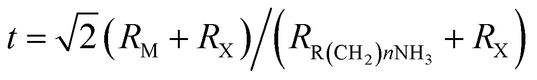 , where RR(CH2)nNH3, RM and RX are the ionic radii of the corresponding substances. In the case that the radii of the organic chain are larger than that of propylamine, an organic–inorganic hybrid R(CH2)nNH3MX4 perovskite will adopt a 2D layered structure.23 Hence, there are on-going efforts to develop 2D layered perovskites in the form of R(CH2)nNH3MX4 monolayers. Such 2D layered organic–inorganic halide R(CH2)nNH3PbX4 perovskite materials exhibit a self-organized quantum-well electronic structure (Fig. 1a), consisting of alternating ∼0.6 nm inorganic layers and ∼1 nm organic layers.24–26 They exhibit strong solar absorption, large exciton binding energies and small Bohr radii, which endow these R(CH2)nNH3PbX4 materials with excellent optical properties, such as sharp resonant emission with a narrow full width at half maximum (FWHM) and a high quantum yield.27 Previous reports have demonstrated that the PL peaks of R(CH2)nNH3MX4 perovskites can be tuned within the visible-infrared range by adjusting the organic component, R; the metal cation, M (M = Pb, Sn, Ge); and the halide, X (X = I, Br, Cl).28–30 Recently, single- and few-layer (C4H9NH3)2PbBr4 single-crystalline perovskite squares have been successfully prepared via a solution-phase growth method. The optical band gap of the 2D square sheets was found to be slightly blue-shifted by 40 meV compared with that of the bulk crystal, but it was otherwise nearly indistinguishable for configurations ranging from 1 to 22 layers.23 In addition, mechanical exfoliation has been applied to produce 2D few-layer (C6H5C2H4NH3)2PbI4 perovskites, in which strong anti-Stokes PL results in laser cooling by ∼58.7 K.31 However, the nature of the excitons in 2D layered R(CH2)nNH3MX4 perovskites is still not well understood.
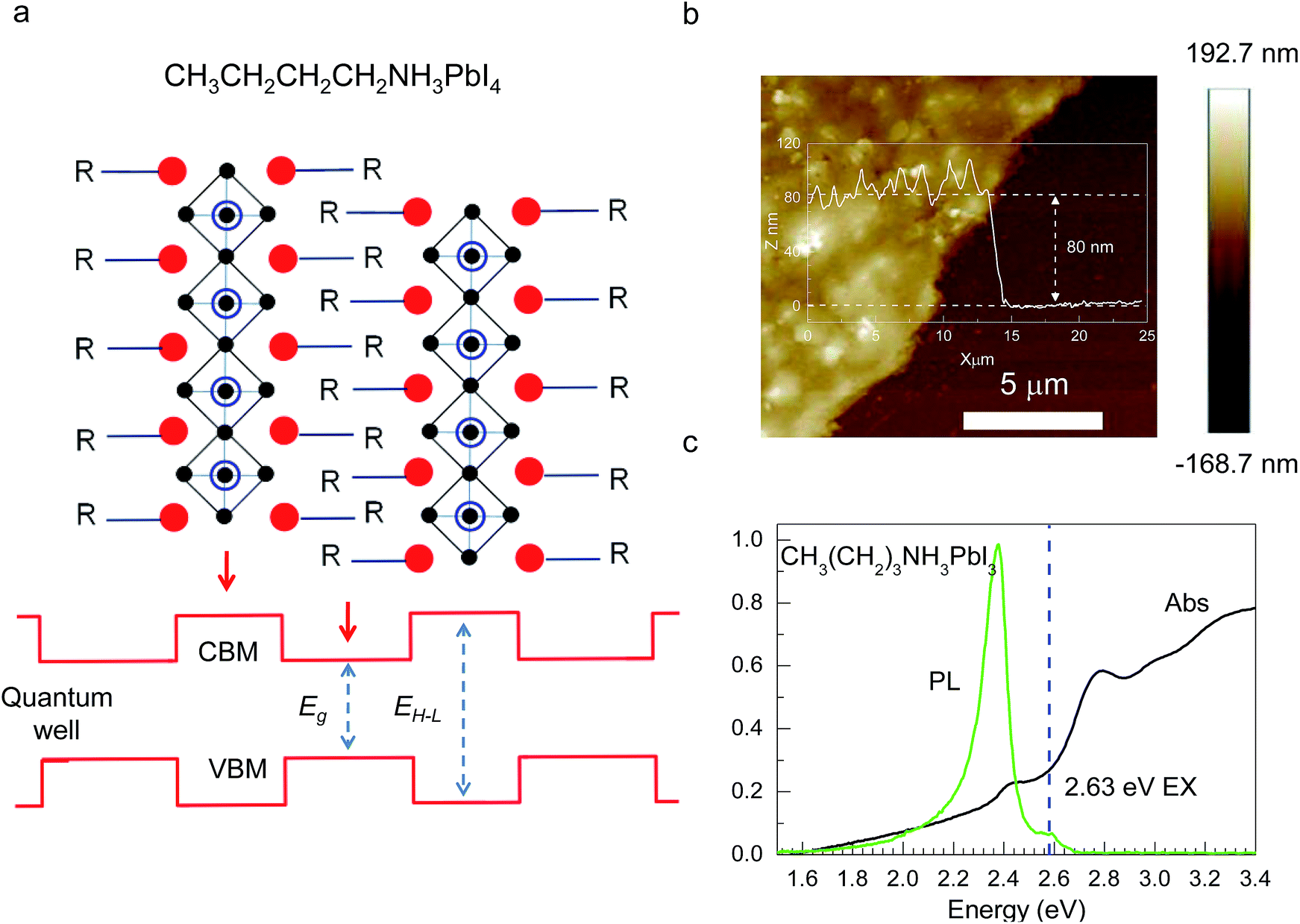 | ||
| Fig. 1 (a) Schematic illustration of 2D layered CH3CH2CH2CH2NH3PbI4 perovskite and its quantum-well electronic structures. (b) AFM image of a CH3CH2CH2CH2NH3PbI4 perovskite film spin coated on quartz. (c) Absorption and photoluminescence spectra of the 2D perovskite at room temperature. | ||
Herein, we investigate the exciton dynamics in 2D layered CH3(CH2)3NH3PbI4 perovskite in the range of 10–300 K by means of PL spectroscopy and two-pulse emission modulation (TPEM) spectroscopy. Interestingly, we find that the variation of the PL peak energy as a function of temperature deviates from Varshni's empirical expression; the phase transition occurs in the range of 200–250 K. Below 200 K, the band gap energy first increases to a maximum of ∼2.374 eV at 150 K but then monotonically drops to ∼2.364 eV at 13 K as the temperature decreases. We demonstrate that Bose–Einstein oscillation contributes to the positive temperature variation of the PL peak energy as a result of free excitons. We also investigate the excitation mechanism of two-photon photoluminescence (TPPL), in which two photons are simultaneously absorbed through a virtual state to excite a single electronic transition. Our work reveals the mechanisms underlying exciton dynamics and excitation in 2D perovskites.
Experiment
CH3(CH2)3NH3I synthesis and film preparation
CH3(CH2)3NH3I was synthesized using the reported method.32 Briefly, 1.5 mL of CH3(CH2)3NH2 was added to 50 mL of ethanol under Ar gas and stirred for 30 min at 0 °C. Subsequently, 1 mL of hydroiodic acid (55 wt% in water, Sigma-Aldrich) was added. The mixed solution was stirred for a further 2 h. The white raw product CH3(CH2)3NH3I was obtained through rotary evaporation at 50 °C, washed three times with diethyl ether, and then finally recrystallized from a mixed solvent of diethyl ether and ethanol. The white solid was dried in vacuum for 24 h and stored in a glovebox. Then, 138 mg of PbI2 and 105 mg of CH3(CH2)3NH3I were dissolved in 2.31 mL of DMF. A volume of 20 μL of the mixed solution was spin coated onto quartz with dimensions of 1 × 1 cm2 at 2000 rpm for 2 min, and the samples were then placed in vacuum for 24 h for the removal of residual DMF solvent.TPPL measurements
The TPPL spectra were measured using a home-built two-photon optical microscope. A mode-locked Ti:sapphire oscillator (TiF-100M, Avesta) was used as the excitation source, generating 80 fs pulses with a central wavelength of 785 nm and repetition rate of 84.5 MHz. The laser beam was passed through a 785/10 nm band-pass filter (LD01-785/10-25, Semrock), 5× spatially expanded, and then reflected by a 50/50 beam splitter to the objective lens (NA = 0.5). The emission signals were collected by the same objective lens and filtered with two 785 nm notch filters (NF03-785E-25, Semrock) to reduce laser scattering and with a long-pass filter with a cut-off wavelength of 450 nm (Chroma) to remove the second-harmonic generation signal. The spectra of the emission signals were measured using a monochromator (Acton SpectraPro 2300i, Princeton Instruments) coupled to a CCD (Pixis 100B, Princeton Instruments) via an optical fibre.TPEM measurements
Two-pulse correlation measurements were performed using a dual-channel regenerative amplifier (ORPHEUS Twins, Light Conversion) pumped by a femtosecond laser oscillator (PHAROS, Light Conversion). This system provided laser pulses centred at 800 nm, with a pulse duration of 200 fs and a repetition rate of 1 MHz. The laser beam was split into two pulse replicas. The two laser pulses were spatially overlapped and focused by an objective (×20) onto the 2D perovskite thin film (the laser pulses were broadened to ∼330 fs after the objective). The TPPL of the 2D perovskite thin film was collected using the same objective and detected by a photomultiplier tube (E717-63, Hamamatsu). The emission was filtered using a 550 nm ± 50 nm band-pass filter and a 700 nm short-pass filters. The two-pulse correlation curve was obtained by varying the time delays between the two pulse replicas through a translational stage (M-ILS250HA, Newport).UV-vis absorption, PL, and AFM measurements
UV-vis absorption data for CH3(CH2)3NH3PbI4 were obtained using a PerkinElmer LAMBDA 750 spectrophotometer. The steady-state PL signal was recorded using a Witec Alpha 300R confocal Raman microscope under 0.67 mW laser excitation at 4.88 eV. The samples were placed in a closed-cycle cryogenic system for low-temperature measurements over a range of 10–300 K. The AFM data were recorded using a BRUKER Dimension FastScan system.Results and discussion
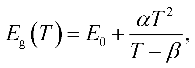
CH3(CH2)3NH3I was synthesized through the reaction of CH3(CH2)3NH3 and HI at 0 °C for 2 h and was then dissolved in dimethylformamide (DMF) with PbI2 (10% wt). The as-grown crystallites were spin coated onto quartz at 2000 rpm for 2 min, and then dried under vacuum for 24 h. An AFM image shows that the thickness of the 2D layered CH3(CH2)3NH3PbI4 films was ∼80 nm (Fig. 1b). Fig. 1c displays the absorption and PL spectra measured for the prepared 2D perovskite films at room temperature. Two obvious absorption features are evident at ∼2.79 and ∼2.43 eV, which are assigned as the band-edge peak and the free-exciton peak,24,30 respectively. Intrinsic free-exciton recombination dominates the PL emission, resulting in a strong PL peak at ∼2.38 eV under laser excitation at 2.63 eV (Fig. 1c).To further clarify the underlying dynamics responsible for the evolution of the free-exciton emission, we plot the evolution of the excitonic energy (normalized PL) as a function of the temperature from 13 to 300 K under laser excitation at 4.88 eV, as shown in Fig. 2a. Surprisingly, an anomalous non-monotonic relationship between the PL peak energy and temperature is observed for the 2D layered CH3(CH2)3NH3PbI4 films. As the temperature decreases from room temperature, the PL peak energy first increases from ∼2.367 eV to a maximum of ∼2.375 eV at 230 K, however sharply drops to ∼2.373 eV at 200 K, which further increases to ∼2.374 eV at 150 K and then monotonically decreases to ∼2.364 eV at 13 K (Fig. 2b). Typically, the PL peak energy monotonically increases as the temperature decreases, as expressed by the Varshni model:33
 | (1) |
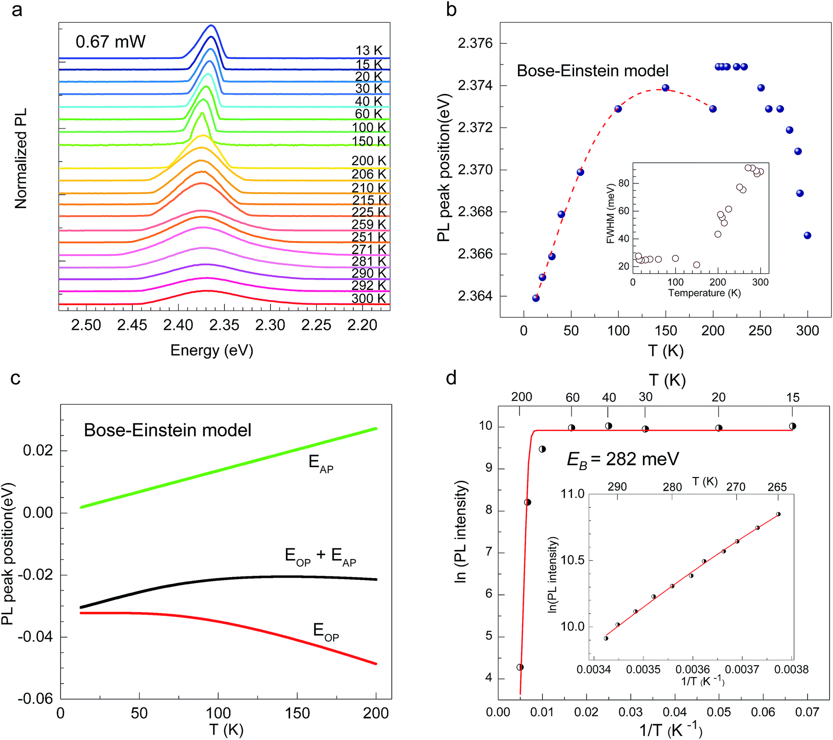 | ||
| Fig. 2 (a) PL spectra of 2D layered CH3CH2CH2CH2NH3PbI4 perovskite for temperatures from 13 to 300 K. (b) PL peak energy vs. temperature, fitted using the Bose–Einstein oscillator model (dashed red curve). The inset show the FWHM as a function of temperature. (c) The optical and acoustic phonon energies as functions of temperature in the Bose–Einstein oscillator model. (d) PL intensity as a function of temperature. The exciton binding energy is ∼282 meV. | ||
Generally, the temperature variation of the PL peak energy has its origins in the effects of lattice thermal expansion (TE) and electron–phonon interaction (EP), which, at constant temperature, can be expressed as follows:42
| (ΔE0)T = (ΔE0)EP + (ΔE0)TE | (2) |
(ΔE0)TE represents the harmonic corrections to the crystal volume at low temperatures, which can be related to the isotope masses through the zero-point vibrational amplitudes, (∂E0/∂Mk)TE. (ΔE0)TE is usually much smaller than (ΔE0)EP; thus, it is justifiable to neglect (ΔE0)TE at low temperatures.43,44 We focus on investigating the exciton dynamics below 200 K, and suggest that the renormalization of the band gap and PL emission stems from electron–phonon interactions that occur below 200 K. In 2D layered perovskites, the valence bands (VBs) consist mainly of the Pb(6s)2 and I(5p)6 orbitals, and the conduction band (CB) is mainly composed of the Pb(6s)(6p) orbital.45,46 The organic component does not play a significant role in determining the electronic structure.41,47 The optical transitions in 2D perovskites thus stem from the 6s to 6p transition in Pb2+, which is similar to that in PbI2. Because Pb(207) has a larger atomic mass than I(126), the Pb atoms undergo Bose–Einstein oscillation at a low frequency that induces acoustic phonons, whereas the I atoms predominantly exhibit high-frequency Bose–Einstein oscillations, resulting in optical phonons. The electron–phonon interactions critically depend on the amplitudes of the phonons and the corresponding coupling constants. Thus, the temperature dependence of the free-exciton emission energy Eg(T) should be related to that of both the optical phonon energy, EOP(T), and the acoustic phonon energy, EAP(T):39,40
 | (3) |
 | (4) |
| Eg(T) = E0 + EOP(T) + EAP(T), | (5) |
Fig. 2d shows the PL intensity as a function of 1/T under laser excitation at 4.88 eV; the plot indicates that the PL intensity first gradually increases and then dramatically decreases as the temperature increases. Under steady-state excitation, the temperature dependence of the PL intensity can be expressed as48
 | (6) |
CH3(CH2)3NH3PbI4 exhibits excellent non-linear optical properties. A home-built two-photon optical microscope was used to investigate the TPPL of CH3(CH2)3NH3PbI4 perovskite.55 Fig. 3 shows the one- and two-photon photoluminescence (OPPL and TPPL) spectra of the 2D layered CH3(CH2)3NH3PbI4 films under pulsed laser excitation at 3.1 and 1.55 eV. The PL intensity shows a linear relationship with the excitation power under optical pumping with 3.1 eV (Fig. 3a and b). Under 1.55 eV excitation, an exponential relationship between PL intensity and excitation power is observed, which can be well fitted using the function y = ax1.8 (Fig. 3c and d), indicating the occurrence of TPPL. Considering the long tails of the absorption spectrum of the 2D layered CH3(CH2)3NH3PbI4 films (Fig. 1c), two possible excitation mechanisms may be responsible for the TPPL, namely, a coherent two-photon absorption process or two sequential one-photon absorption processes. The schematic excitation diagrams of these processes are displayed in Fig. 4, respectively. In the coherent two-photon absorption model, two photons are absorbed simultaneously to drive a single electron from the VB into the CB via a virtual intermediate state (Fig. 4a). In the sequential one-photon absorption model, two photons are absorbed sequentially, mediated by a real intermediate state between the VB and CB (Fig. 4b).
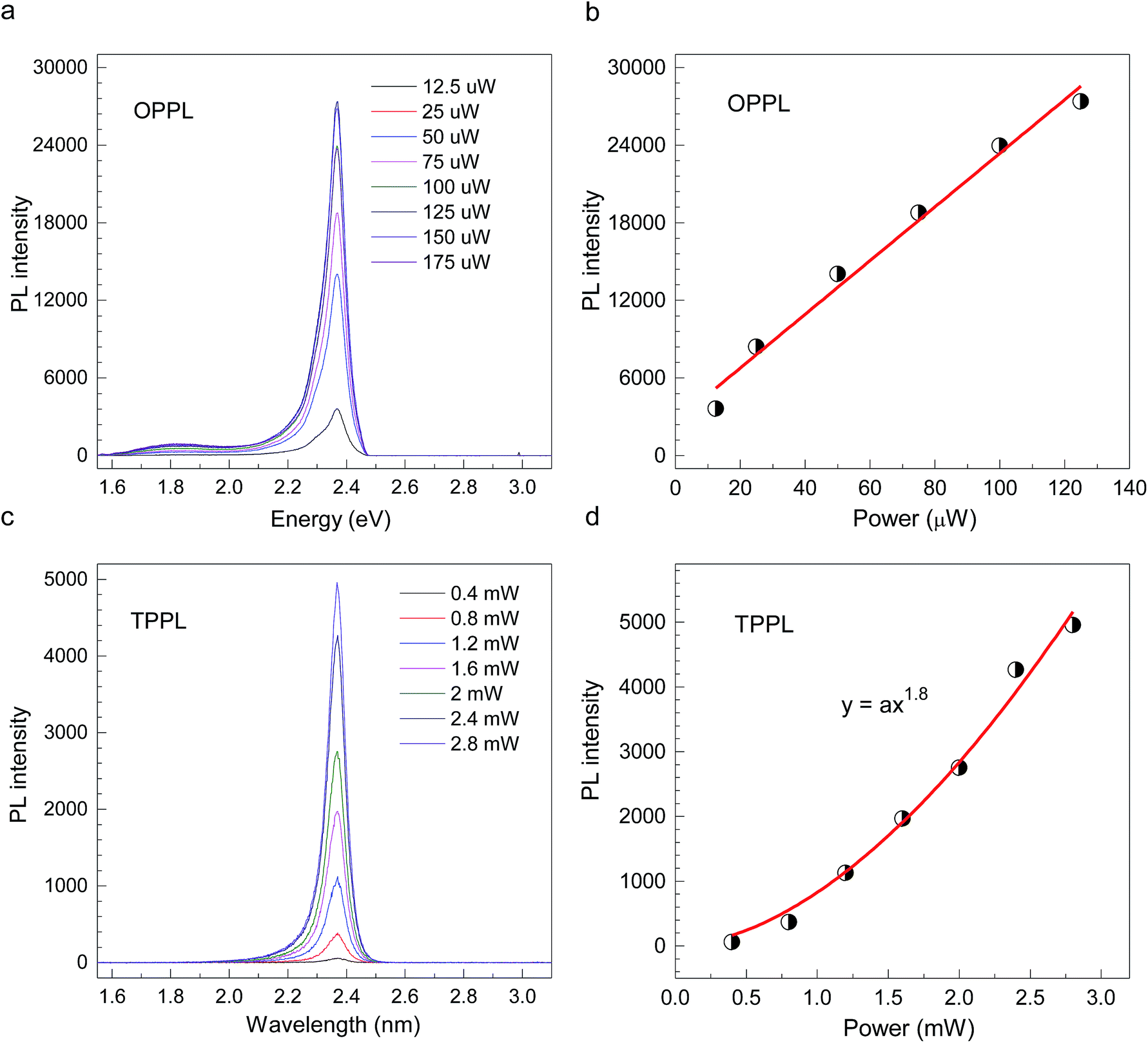 | ||
| Fig. 3 (a and b) OPPL spectra and (c and d) TPPL spectra of 2D layered CH3CH2CH2CH2NH3PbI4 perovskite films at room temperature. | ||
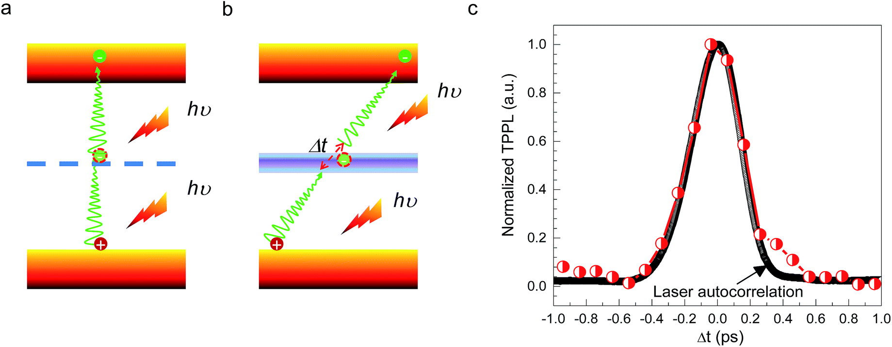 | ||
| Fig. 4 (a and b) Schematic illustrations of two excitation mechanisms: (a) coherent two-photon absorption through a virtual state and (b) two sequential one-photon absorptions through real intermediate states. (c) TPEM measurement of 2D layered CH3CH2CH2CH2NH3PbI4 perovskite (BAPI) at room temperature. | ||
To investigate the TPPL excitation mechanism of the 2D layered CH3(CH2)3NH3PbI4 films, two-pulse emission modulation (TPEM) measurements were conducted to probe the correlated effects of two pulses on the observed PL emission.56 Two 1.55 eV femtosecond laser pulses with similar power were focused onto a 2D layered CH3(CH2)3NH3PbI4 film with a good spatial overlap. The TPPL intensity was recorded as a function of the time delay (Δt) between the two laser pulses. In this configuration, the recorded TPPL emission has two possible origins: (1) two photons from the same laser excitation pulse and (2) two photons from different excitation pulses. It is easy to see that the contribution from the former process is independent of the time delay between two laser pulses, as the excitation photons originate from the same pulse. By contrast, the latter represents the cross-contribution of two individual laser pulses to the TPPL; thus, its contribution is maximal when the two pulses temporally overlap and decreases in intensity as they temporally separate. In the case of the coherent two-photon absorption model, the TPEM curve should show the same profile as that of the laser pulses because the emission originates from the simultaneous absorption of two photons through a virtual state. In the case of sequential one-photon excitations, the two one-photon excitation processes occur at the time scale of the lifetime of the real intermediate state; consequently, the TPEM dynamics should follow the lifetime of the intermediate state, similar to our previous reported TPPL excitation mechanism of gold nanorods.56 As shown in Fig. 4c, the measured TPEM curve of CH3(CH2)3NH3PbI4 perovskite exhibits a FWHM of ∼360 fs, which is consistent with the laser autocorrelation profile. These results suggest that the TPPL in CH3(CH2)3NH3PbI4 perovskite is excited through the coherent two-photon absorption mechanism (Fig. 4a).
Conclusions
In 2D layered CH3(CH2)3NH3PbI4 perovskite films, we observed a non-monotonic temperature variation of the PL peak energy in which the acoustic phonon energy exhibits a positive temperature variation, which is attributed to Bose–Einstein oscillation, whereas the optical phonon energy displays the opposite behaviour. The dielectric confinement effect due to the quantum-well structure of the material strengthens the Coulomb interaction between an electron and a hole, imparting the CH3(CH2)3NH3PbI4 perovskite with a large exciton binding energy of ∼282 meV and thus providing an opportunity to study the exciton dynamics. The nonlinear optical properties of TPPL in 2D layered CH3(CH2)3NH3PbI4 perovskite were also observed, and we confirmed that the excitation is driven by a coherent two-photon absorption mechanism. The strong electron–phonon interactions and large exciton binding energy in 2D layered CH3(CH2)3NH3PbI4 perovskite suggest its potential for use for high-efficiency excitonic energy transfer in lighting and display applications.Author contributions
B. P. and K. P. L. conceived and supervised the experiment. B. P. synthesized CH3(CH2)3NH3PbI4 perovskites. H. Z. and Q. X. carried out two photon PL measurements and TPEM measurement. J. L., Y. L., L. B., H. L., J. X., L. D., L. Z., X. W. carried out the absorption and low temperature PL measurement. All authors discussed the results and wrote the manuscript.Acknowledgements
B. P. acknowledges financial support from National Science Foundation of China (51602040) and Scientific Research Foundation for new teachers of University of Electronic Science and Technology of China (ZYGX2015KYQD057, A03013023601007). K. P. L. thanks A* star-DST project number 1425203139 “Flexible and high performance perovskite based solar cells on grapheme electrodes”.Notes and references
- G. Xing, N. Mathews, S. Sun, S. S. Lim, Y. M. Lam, M. Grätzel, S. Mhaisalkar and T. C. Sum, Science, 2013, 342, 344–347 CrossRef CAS PubMed.
- M. A. Green, A. Ho-Baillie and H. J. Snaith, Nat. Photonics, 2014, 8, 506–514 CrossRef CAS.
- J.-H. Im, I.-H. Jang, N. Pellet, M. Grätzel and N.-G. Park, Nat. Nanotechnol., 2014, 9, 927–932 CrossRef CAS PubMed.
- A. Kojima, K. Teshima, Y. Shirai and T. Miyasaka, J. Am. Chem. Soc., 2009, 131, 6050–6051 CrossRef CAS PubMed.
- M. Liu, M. B. Johnston and H. J. Snaith, Nature, 2013, 501, 395–398 CrossRef CAS PubMed.
- A. Marchioro, J. Teuscher, D. Friedrich, M. Kunst, R. van de Krol, T. Moehl, M. Gratzel and J.-E. Moser, Nat. Photonics, 2014, 8, 250–255 CrossRef CAS.
- C. S. Ponseca, T. J. Savenije, M. Abdellah, K. Zheng, A. Yartsev, T. Pascher, T. Harlang, P. Chabera, T. Pullerits, A. Stepanov, J.-P. Wolf and V. Sundström, J. Am. Chem. Soc., 2014, 136, 5189–5192 CrossRef CAS PubMed.
- S. D. Stranks, G. E. Eperon, G. Grancini, C. Menelaou, M. J. P. Alcocer, T. Leijtens, L. M. Herz, A. Petrozza and H. J. Snaith, Science, 2013, 342, 341–344 CrossRef CAS PubMed.
- M. M. Lee, J. Teuscher, T. Miyasaka, T. N. Murakami and H. J. Snaith, Science, 2012, 338, 643–647 CrossRef CAS PubMed.
- Y. Hu, J. Schlipf, M. Wussler, M. L. Petrus, W. Jaegermann, T. Bein, P. Müller-Buschbaum and P. Docampo, ACS Nano, 2016, 10, 5999–6007 CrossRef CAS PubMed.
- Best Research-Cell Efficiencies, http://www.nrel.gov/ncpv/images/efficiency_chart.jpg, 2016.
- N. J. Jeon, J. H. Noh, W. S. Yang, Y. C. Kim, S. Ryu, J. Seo and S. I. Seok, Nature, 2015, 517, 476–480 CrossRef CAS PubMed.
- J. Burschka, N. Pellet, S.-J. Moon, R. Humphry-Baker, P. Gao, M. K. Nazeeruddin and M. Gratzel, Nature, 2013, 499, 316–319 CrossRef CAS PubMed.
- Y. Wang, X. Li, J. Song, L. Xiao, H. Zeng and H. Sun, Adv. Mater., 2015, 27, 7101–7108 CrossRef CAS PubMed.
- L. Protesescu, S. Yakunin, M. I. Bodnarchuk, F. Krieg, R. Caputo, C. H. Hendon, R. X. Yang, A. Walsh and M. V. Kovalenko, Nano Lett., 2015, 15, 3692–3696 CrossRef CAS PubMed.
- S. Sun, D. Yuan, Y. Xu, A. Wang and Z. Deng, ACS Nano, 2016, 10, 3648–3657 CrossRef CAS PubMed.
- J. Song, J. Li, X. Li, L. Xu, Y. Dong and H. Zeng, Adv. Mater., 2015, 27, 7162–7167 CrossRef CAS PubMed.
- W. Niu, A. Eiden, G. Vijaya Prakash and J. J. Baumberg, Appl. Phys. Lett., 2014, 104, 171111 CrossRef.
- S. T. Ha, X. Liu, Q. Zhang, D. Giovanni, T. C. Sum and Q. Xiong, Adv. Opt. Mater., 2014, 2, 838–844 CrossRef CAS.
- Q. Zhang, S. T. Ha, X. Liu, T. C. Sum and Q. Xiong, Nano Lett., 2014, 14, 5995–6001 CrossRef CAS PubMed.
- Q. Liao, K. Hu, H. Zhang, X. Wang, J. Yao and H. Fu, Adv. Mater., 2015, 27, 3405–3410 CrossRef CAS PubMed.
- J. Liu, Y. Xue, Z. Wang, Z.-Q. Xu, C. Zheng, B. Weber, J. Song, Y. Wang, Y. Lu, Y. Zhang and Q. Bao, ACS Nano, 2016, 10, 3536–3542 CrossRef CAS PubMed.
- L. Dou, A. B. Wong, Y. Yu, M. Lai, N. Kornienko, S. W. Eaton, A. Fu, C. G. Bischak, J. Ma, T. Ding, N. S. Ginsberg, L.-W. Wang, A. P. Alivisatos and P. Yang, Science, 2015, 349, 1518–1521 CrossRef CAS PubMed.
- X. Hong, T. Ishihara and A. V. Nurmikko, Phys. Rev. B: Condens. Matter Mater. Phys., 1992, 45, 6961–6964 CrossRef CAS.
- D. B. Mitzi, J. Chem. Soc., Dalton Trans., 2001, 1–12, 10.1039/b007070j.
- C. C. Stoumpos, D. H. Cao, D. J. Clark, J. Young, J. M. Rondinelli, J. I. Jang, J. T. Hupp and M. G. Kanatzidis, Chem. Mater., 2016, 28, 2852–2867 CrossRef CAS.
- K. Gauthron, J. S. Lauret, L. Doyennette, G. Lanty, A. Al Choueiry, S. J. Zhang, A. Brehier, L. Largeau, O. Mauguin, J. Bloch and E. Deleporte, Opt. Express, 2010, 18, 5912–5919 CrossRef CAS PubMed.
- D. B. Mitzi, Chem. Mater., 1996, 8, 791–800 CrossRef CAS.
- D. B. Mitzi, Inorg. Chem., 2000, 39, 6107–6113 CrossRef CAS PubMed.
- D. B. Mitzi, D. R. Medeiros and P. R. L. Malenfant, Inorg. Chem., 2002, 41, 2134–2145 CrossRef CAS PubMed.
- S.-T. Ha, C. Shen, J. Zhang and Q. Xiong, Nat. Photonics, 2016, 10, 115–121 CrossRef CAS.
- L. Etgar, P. Gao, Z. Xue, Q. Peng, A. K. Chandiran, B. Liu, M. K. Nazeeruddin and M. Grätzel, J. Am. Chem. Soc., 2012, 134, 17396–17399 CrossRef CAS PubMed.
- Y. P. Varshni, Physica, 1967, 34, 149–154 CrossRef CAS.
- J. Zhang, D. Li, R. Chen and Q. Xiong, Nature, 2013, 493, 504–508 CrossRef CAS PubMed.
- S. Tongay, J. Zhou, C. Ataca, K. Lo, T. S. Matthews, J. Li, J. C. Grossman and J. Wu, Nano Lett., 2012, 12, 5576–5580 CrossRef CAS PubMed.
- Y. J. Lu, J. Kim, H. Y. Chen, C. H. Wu, N. Dabidian, C. E. Sanders, C. Y. Wang, M. Y. Lu, B. H. Li, X. G. Qiu, W. H. Chang, L. J. Chen, G. Shvets, C. K. Shih and S. Gwo, Science, 2012, 337, 450–453 CrossRef CAS PubMed.
- J. S. Ross, S. Wu, H. Yu, N. J. Ghimire, A. M. Jones, G. Aivazian, J. Yan, D. G. Mandrus, D. Xiao, W. Yao and X. Xu, Nat. Commun., 2013, 4, 1474 CrossRef PubMed.
- J. Huang, T. B. Hoang and M. H. Mikkelsen, Sci. Rep., 2016, 6, 22414 CrossRef CAS PubMed.
- J. Bhosale, A. K. Ramdas, A. Burger, A. Muñoz, A. H. Romero, M. Cardona, R. Lauck and R. K. Kremer, Phys. Rev. B: Condens. Matter Mater. Phys., 2012, 86, 195208 CrossRef.
- V. D'Innocenzo, G. Grancini, M. J. P. Alcocer, A. R. S. Kandada, S. D. Stranks, M. M. Lee, G. Lanzani, H. J. Snaith and A. Petrozza, Nat. Commun., 2014, 5, 3586 Search PubMed.
- T. Ishihara, J. Takahashi and T. Goto, Phys. Rev. B: Condens. Matter Mater. Phys., 1990, 42, 11099–11107 CrossRef CAS.
- A. Göbel, T. Ruf, M. Cardona, C. T. Lin, J. Wrzesinski, M. Steube, K. Reimann, J. C. Merle and M. Joucla, Phys. Rev. B: Condens. Matter Mater. Phys., 1998, 57, 15183–15190 CrossRef.
- S. Ozaki and Y. Horikoshi, J. Appl. Phys., 2014, 115, 053526 CrossRef.
- M. Cardona and M. L. W. Thewalt, Rev. Mod. Phys., 2005, 77, 1173–1224 CrossRef CAS.
- T. Kenichiro, T. Takayuki, K. Takashi, U. Kenichi, E. Kazuhiro, U. Tsutomu, A. Keisuke, U. Kazuhito and M. Noboru, Jpn. J. Appl. Phys., 2005, 44, 5923 CrossRef.
- J. Even, L. Pedesseau, M. A. Dupertuis, J. M. Jancu and C. Katan, Phys. Rev. B: Condens. Matter Mater. Phys., 2012, 86, 205301 CrossRef.
- D. Giovanni, W. K. Chong, H. A. Dewi, K. Thirumal, I. Neogi, R. Ramesh, S. Mhaisalkar, N. Mathews and T. C. Sum, Sci. Adv., 2016, 2, e1600477 Search PubMed.
- M. Leroux, N. Grandjean, B. Beaumont, G. Nataf, F. Semond, J. Massies and P. Gibart, J. Appl. Phys., 1999, 86, 3721–3728 CrossRef CAS.
- G. Xing, N. Mathews, S. S. Lim, N. Yantara, X. Liu, D. Sabba, M. Grätzel, S. Mhaisalkar and T. C. Sum, Nat. Mater., 2014, 13, 476–480 CrossRef CAS PubMed.
- B. Peng, G. Yu, X. Liu, B. Liu, X. Liang, L. Bi, L. Deng, T. C. Sum and K. P. Loh, 2D Mater., 2016, 3, 025020 CrossRef.
- B. Peng, G. Yu, Y. Zhao, Q. Xu, G. Xing, X. Liu, D. Fu, B. Liu, J. R. S. Tan, W. Tang, H. Lu, J. Xie, L. Deng, T. C. Sum and K. P. Loh, ACS Nano, 2016, 10, 6383–6391 CrossRef CAS PubMed.
- B. Peng, Q. Zhang, X. F. Liu, Y. Ji, H. V. Demir, C. H. A. Huan, T. C. Sum and Q. H. Xiong, ACS Nano, 2012, 6, 6250–6259 CrossRef CAS PubMed.
- B. Peng, X. Lu, S. Chen, C. H. A. Huan, Q. Xiong, E. Mutlugun, H. V. Demir and S. F. Yu, Nano Res., 2016, 9, 549–559 CrossRef CAS.
- B. Peng, Z. Li, E. Mutlugun, P. L. Hernandez Martinez, D. Li, Q. Zhang, Y. Gao, H. V. Demir and Q. Xiong, Nanoscale, 2014, 6, 5592–5598 RSC.
- M. Garai, T. Zhang, N. Gao, H. Zhu and Q.-H. Xu, J. Phys. Chem. C, 2016, 120, 11621–11630 CAS.
- X.-F. Jiang, Y. Pan, C. Jiang, T. Zhao, P. Yuan, T. Venkatesan and Q.-H. Xu, J. Phys. Chem. Lett., 2013, 4, 1634–1638 CrossRef CAS PubMed.
| This journal is © The Royal Society of Chemistry 2017 |