
 Open Access Article
 This Open Access Article is licensed under a
 Creative Commons Attribution 3.0 Unported Licence
A moderate synthesis route of 5.6 mA-current LaB6 nanowire film with recoverable emission performance towards cold cathode electron source applications
Haibo Gan†
,
Luxi Peng†,
Xun Yang,
Yan Tian,
Ningsheng Xu,
Jun Chen,
Fei Liu * and
Shaozhi Deng*
* and
Shaozhi Deng*
State Key Laboratory of Optoelectronic Materials and Technologies, Guangdong Province Key Laboratory of Display Material and Technology, School of Electronics and Information Technology, Sun Yat-sen University, Guangzhou 510275, PR China. E-mail: liufei@mail.sysu.edu.cn; stsdsz@mail.sysu.edu.cn
First published on 9th May 2017
Abstract
Lanthanum hexaboride (LaB6) nanostructures have attracted much attention in recent years because they exhibit high electrical conductivity and thermal conductivity, low work function and high chemical stability, and can be expected to be an ideal cold cathode electron source for power device applications. Although some groups have developed means to grow LaB6 nanostructures and investigated their emission properties, the moderate synthesis of the LaB6 nanostructure cathode with high-performance is still a challenging issue. Here we developed a simple one-step chemical vapour deposition (CVD) method to prepare the LaB6 nanowire cold cathode film. The LaB6 nanowires have a mean length of tens of micrometres and their average diameter is about 100 nm. The formation of the nanowires is attributed to the synergy of the vapour–liquid–solid (VLS) and vapour–solid (VS) mechanisms. The LaB6 nanowires are found to have a low turn-on (2.2 V μm−1) and threshold field (2.9 V μm−1) as well as nice field emission (FE) stability with a current fluctuation of only 1.7%. And their emission current can reach 5.6 mA (16.7 mA cm−2) at 4.1 V μm−1, which is large enough for the high-current requirements of cathodes used in power devices. Moreover, the LaB6 nanowires still retain excellent performance even if the operation temperature is raised up to 773 K. It is noted that the LaB6 nanowire film exhibits quite different emission behaviours during a temperature cycling between room temperature and 773 K. The adsorption and desorption of oxygen onto and from the nanowire's surface is suggested to explain the discrepancy of such emission properties based on a series of our designed experiments. Most importantly, the LaB6 nanowire cathode film can almost recover to the original excellent FE performances after detachment of the surface oxygen molecules, which suggests that they should be ideal cathode nanomaterials for power device applications.
Introduction
LaB6 has attracted intense attention in the past few years because of its unique characteristics, such as high melting-point (2715 °C), large electrical conductivity (1.7 or 3 × 10⁻⁵ Ω cm) and thermal conductivity (110 W (m−1 K−1)), low work function (∼2.67 eV) and strong endurance to harsh environments.1–4 Because the LaB6-based thermal electron gun can produce a very large emission current (23 A) and current density (20 A cm−2) at high voltage and high temperature,5 it is very popular as a thermal electron source material. In comparison to the thermal emission, the field emission (FE) can operate at room temperature without any time delay and external heating source, which is suitable for cold cathode electron sources. Considering that LaB6 possesses the required excellent properties of cold cathode materials, many researchers endeavour to explore their potential applications in high-current cold cathode devices. It is known that microwave tubes and X-ray tube devices demand high-current (over 0.1 A) cathode electron sources.6,7 Even for the THz devices with low-current requirements, the electron source must possess at least a mA emission current.6,8 In comparison with their bulk counterparts, the LaB6 nanostructures have larger aspect ratios, and thus they should be more suitable for high-current cold cathode electron sources. Recently, a low-noise and high-resolution images has been acquired by a modified scanning electron microscope (SEM),9 in which a single LaB6 nanowire was used as a cold cathode electron source. It also arouses the renewed interests of the researchers on the high-current performances of LaB6 nanostructures.As known to all, most reports focused on the growth and room-temperature FE properties of the LaB6 nanostructures,10–16 only a few researches concerned on their FE properties at different operation temperatures.17,18 Because the research on the FE properties of the LaB6 structures at variable temperature is very essential for cold cathode electron sources, the lack of the relevant researches will prevent them from rapid developments in cold cathode devices. In addition, it is found that either the poisonous liquid or inflammable gas is usually chosen as boron sources in all existing procedures for synthesis of the LaB6 nanostructures.10,11,13,16,18 The use of the poisonous or inflammable sources not only inevitably produces pollution to the environment but also increases the production cost. So it becomes a great challenge for the researchers to find a cheap and moderate way to prepare the LaB6 nanostructures with high-current FE performances at various temperatures.
In this paper, we developed a simple and moderate method to synthesize LaB6 nanowire film with high-current performance. Moreover, the FE properties of the LaB6 nanowire film at varied ambient temperature will be compared to evaluate their feasibility in cold cathode electron source applications. Finally, a possible FE mechanism is proposed to explain their different emission behaviours during cycling of the temperature between the room temperature and 773 K.
Experimental section
The LaB6 nanowire film was prepared by a low-pressure CVD method in a tube-furnace, as described in our recent studies.19–21 The mixed powders of B, B2O3 and LaCl3 were used as source materials, all of which are nontoxic and low-cost. And then they were loaded into a vessel and placed into the central region of the furnace. A 10 nm Ni film was deposited onto the surface of heavily-doped p-type Si substrate as the catalysts by magnetron-sputtering way. The synthesis of the LaB6 nanowires can be depicted as follows. Firstly, the furnace was rapidly heated to 700 °C and kept for one hour under the mixed gas of Ar and H2. The ratio between the flow rates of Ar and H2 was kept at 285 sccm![[thin space (1/6-em)]](https://www.rsc.org/images/entities/char_2009.gif) :200 sccm in this step. Secondly, when the temperature reached 1100 °C, the growth of the LaB6 nanowires was initiated. In this stage, the flow rate of Ar to H2 were adjusted to be 285 sccm and 10 sccm, respectively. The chamber pressure was kept at about 0.2 kPa, and the reaction lasted for about half an hour. Finally, a dark-blue film was found on the surface of the Si substrate after the furnace was cooled down to room temperature in flowing Ar ambient.
:200 sccm in this step. Secondly, when the temperature reached 1100 °C, the growth of the LaB6 nanowires was initiated. In this stage, the flow rate of Ar to H2 were adjusted to be 285 sccm and 10 sccm, respectively. The chamber pressure was kept at about 0.2 kPa, and the reaction lasted for about half an hour. Finally, a dark-blue film was found on the surface of the Si substrate after the furnace was cooled down to room temperature in flowing Ar ambient.
X-ray diffractometer (Rigaku, D-MAX 2200 VPC) and Raman spectroscope (Renishaw, Invia Reflex) were used to ascertain the chemical compositions of the products. The morphology and crystalline structure of the sample were respectively characterized by scanning electron microscope (SEM, Zeiss, SUPER-55) and transmission electron microscope (TEM, FEI, Titan3 G2 60-300). The surface compositions of the sample were investigated by X-ray photoelectron spectrometer (XPS, Thermo Fisher, ESCALAB 250Xi). The conductivity and FE characteristics of a single nanowire were in situ studied on our modified SEM system.19,20 The FE measurements of the LaB6 nanowire film at different temperature or in oxygen ambient of varied partial pressure were performed in our self-built FE analysis and measurement system.
Results and discussion
By choosing the cheap and nontoxic B, B2O3 and LaCl3 powders as the source materials, aligned LaB6 nanowires have been successfully fabricated on a heavily-doped p-type Si substrate. Typical SEM images of the as-grown nanowires are shown in Fig. 1(a)–(c). As in Fig. 1(a), the nanowires exhibit a uniform morphology and are adhered to the substrate with tilting angles ranging from 50° to 80°. In addition, the nanowires are seen to have a smooth surface and uniformly distributed all over the substrate (Fig. 1(b)). One can see in Fig. 1(c) that the averaged diameter and length of the nanowires are 100 nm and tens of micrometres, respectively. The aspect ratio of the as-prepared nanowires reaches several hundred, which can be helpful for their low-field FE operation. If the chamber pressure and growth time were further increased, the length of nanowires can reach as long as several millimetres.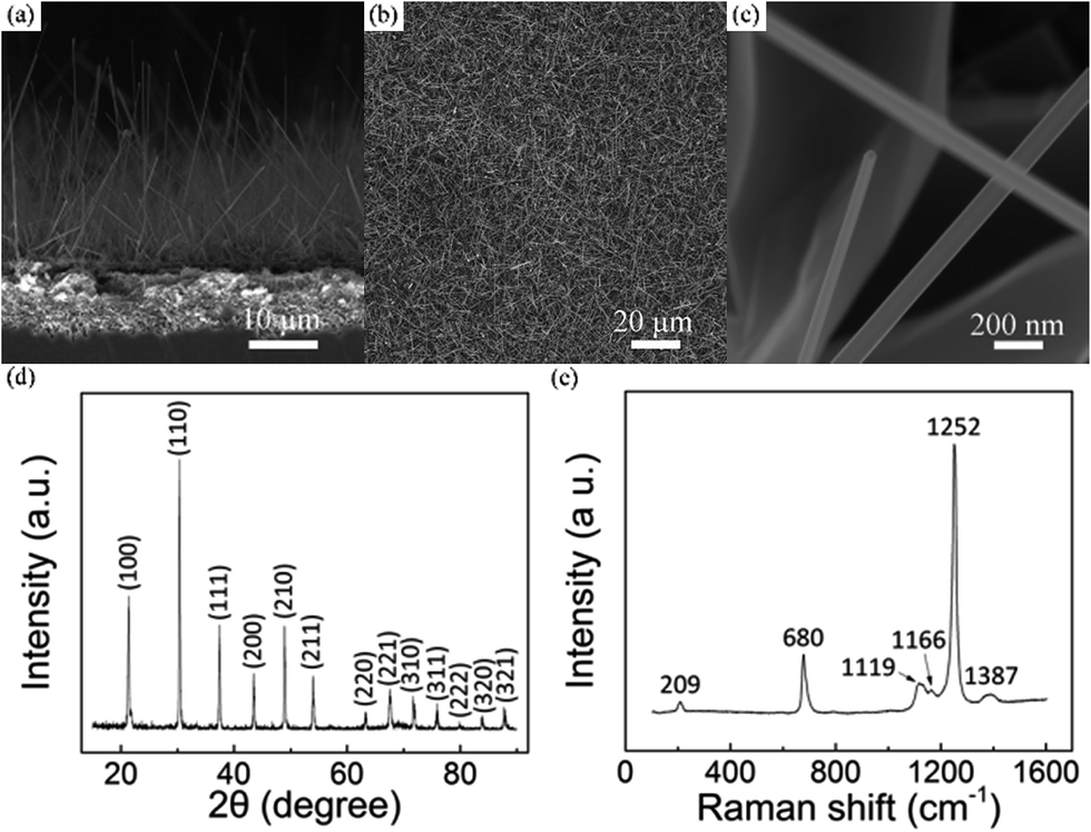 | ||
| Fig. 1 (a and b) Typical low- and high-resolution SEM images of LaB6 nanowires. (c) The cross-section image of LaB6 nanowires. (d and e) Typical XRD pattern and Raman spectroscopy of LaB6 nanowire film. | ||
To ascertain the chemical compositions of the as-prepared nanowires, X-ray diffraction (XRD) and Raman spectroscopy techniques were respectively performed on the sample. One can see in Fig. 1(d) that all of the diffraction peaks agree to LaB6 phase well according to the data from the Joint Committee for Powder Diffraction Standards (JCPDS) card no. 73-1669. No impurity phase appears in this pattern, suggesting that the sample is pure LaB6 crystal. Fig. 1(e) gives the representative Raman spectrum of the sample. There are five characteristic peaks in this spectrum, which are respectively 209, 680, 1119, 1166, 1252 and 1387 cm−1. The Raman peaks of the sample also conform to bulk LaB6 as well as nanostructures reported previously.18,22–24 As explained in these studies, the peak at 209 cm−1 may originate from the vibration of the La ions in the cage formed by B6 molecule.18,23 The peak at 680 cm−1 belongs to T2g vibrational mode, and the peak at 1387 cm−1 results from the second-order excitation of the T2g mode.18,22–24 The peaks at 1119 and 1166 cm−1 come from Eg mode, and the peak at 1252 cm−1 originates from A1g mode.18,22–24 Based on the XRD and Raman results, the as-prepared nanowires can be confirmed to be LaB6 crystals.
Typical low- and high-magnification TEM images of the LaB6 nanowire were respectively given in Fig. 2(a) and (b) to further ascertain their crystallinity and growth direction. The inset is the corresponding selected-area electron diffraction (SAED) pattern, in which one can see that the diffraction spots are very sharp and clear. It is seen in Fig. 2(a) that the nanowire has a smooth configuration. As shown in Fig. 2(b), the lattice distance between adjacent crystalline planes is about 0.42 nm, which is in good agreement with the interplanar spacing of the cubic LaB6 crystal along the [111] direction. It is also found in Fig. 2(b) that a very thin amorphous shell exists on the surface of the nanowire and its thickness is usually less than 1 nm. The energy dispersive X-ray (EDX) spectrum of the nanowire is given in Fig. 2(c) to analyse its compositions, in which one can see that the nanowire is mainly consisted of La and B elements (>98%). The O and Si contents are very tiny, as found in this spectrum. The Cu signal results from the TEM grid, and Si element should originate from the Si substrate. The O signal may come from the adsorbed oxygen molecules or amorphous oxide shell on the nanowire surface, which is likely formed upon exposure of the nanowires to the air after the growth process. To further confirm the element distribution of the nanowire, the EDX line scanning of the nanowire was provided in Fig. 2(d). The result reveals that the La and B elements uniformly distribute throughout the whole nanowire whereas the O element only exists at the sheath of the nanowire. Combined the TEM with EDX results, it can be concluded that the nanowire is single crystalline LaB6 with a growth orientation along the [111] direction.
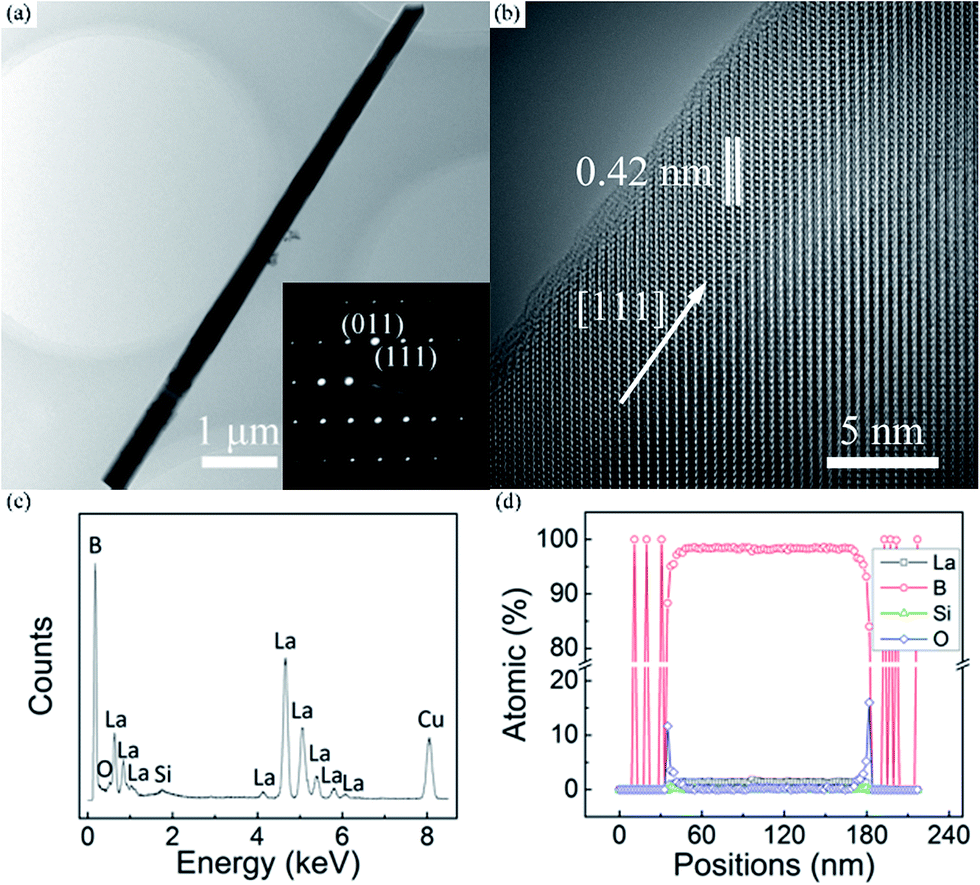 | ||
| Fig. 2 (a and b) Low- and high-resolution TEM image of LaB6 nanowire, and the corresponding SAED pattern is given in the inset. (c and d) EDX spectrum and element distribution curve of the LaB6 nanowire. The inset gives the corresponding scanning area of the nanowire, as referred by the yellow line. | ||
Although the Ni catalysts are used in the growth process of the LaB6 nanowires, the traditional VLS mechanism can't be directly used to illustrate their formation in our work. Based on our experiment results, the synergy of the VLS and VS mechanisms should be responsible for the growth of the LaB6 nanowires. The possible process is depicted as follows. Firstly, when the temperature is raised to 1000 °C, the B2O2 vapour is generated by the reaction of B and B2O3 powders, which will be transferred to the substrate region. Secondly, the B2O2 vapour reacts with the LaCl3 vapour and produces the LaB6 solids on the surface of the Si substrate with the help of the Ni catalysts. In this step, the VLS mechanism dominates over the formation of the LaB6 solids. Thirdly, the following LaCl3 and B2O2 vapour continuously reacts with each other in the high-temperature region and deposit on the surface of the LaB6 solids. The LaB6 solids act as the seed for the growth of the nanowire. Subsequently, the nanowires grow along the energetically-favourable direction via the VS mechanism. In this step, the Ni nanoparticles can't play a catalytic role. It is reasonable that nearly all the Ni nanoparticles are encapsulated or buried by the LaB6 solids and lost the catalysis ability in the second procedure, as found in our experiments. Finally, the LaB6 nanowires are formed on the Si substrate with the proceeding of the reaction. Therefore, it can be comprehensible that the growth of the LaB6 nanowires should be attributed to be the synergy of the VLS and VS mechanisms rather than the VLS mechanism.
The bulk LaB6 crystals are believed to be conductors, while the conductivity of the LaB6 nanowires is seldom concerned despite of which is very important for their power device applications. Here, in situ measurement technique is applied to investigate the conductivity of individual LaB6 nanowires, as described in our recent works.25 In a specific measurement, the tungsten probe is utilized as anode and an individual LaB6 nanowire is selected as cathode, which are tightly contacted for I–V measurements. For the FE measurements, the probe and nanowire are kept several micrometres away using the piezoelectric nanomotor. We randomly choose three nanowires as the research goals, and Fig. 3(a) and (c) respectively give the SEM images of a single LaB6 nanowire during the I–V and FE measurements. Typical I–V curves of three individual LaB6 nanowires are shown in Fig. 3(b). It is obviously seen that the I–V curves of these individual LaB6 nanowires are linear, which suggest nice ohmic contacts exist between probe and nanowire. One can also see that the slopes of the I–V curves of three individual nanowires are not equal, which suggest that the electric resistances of the nanowires are different. Such differences should come from the discrepancy of the length and diameter of the nanowires, because the length of nanowire_1, nanowire_2 and nanowire_3 is respectively 19.7, 23.4 and 16.9 μm and their diameter is 263, 243 and 232 nm. It is found that the resistivity of nanowire_1 (7.2 × 10⁻⁵ Ω cm), nanowire_2 (9.4 × 10⁻⁵ Ω cm) and nanowire_3 (1.2 × 10⁻⁴ Ω cm) is very close despite that their resistances are different. Thus the averaged resistivity of LaB6 nanowires is calculated to be about 9.5 × 10⁻⁵ Ω cm, which is very close to the room-temperature resistivity of the bulk LaB6. It can be concluded that the LaB6 nanowires prepared by our method are the same excellent conductors as their bulk counterparts. Furthermore, we measured the FE properties of these three individual LaB6 nanowires, and their representative J–E curves are shown in Fig. 3(d). It is found that all of these three LaB6 nanowires exhibit the maximum emission current of over 40 μA. Among them, the highest emission current of individual LaB6 nanowire can reach as high as 96.0 μA. It is also found that the FE curves of these three individual nanowires exhibit different evolvements, which should originate from the differences of their electric resistances as well as the distances between the nanowire and tungsten probe. The area (S) of the cross-section of an individual LaB6 can be calculated by S = πr2, in which r is the tip radius of the nanowire. Considering that r is about 14 nm, the highest current density of a single LaB6 nanowire can arrive at 1.6 × 10⁷ A cm−2. Table 1 summarizes the FE properties of some individual nanomaterials with excellent emission performances. It is clearly seen that the emission behaviours of individual LaB6 nanowires are far better than those of most of the nanomaterials26–28 and it is even comparable to those of the vertically-aligned CNT.29 Therefore, it is suggested that the LaB6 nanowires should be one of the most excellent cold cathode nanomaterials.
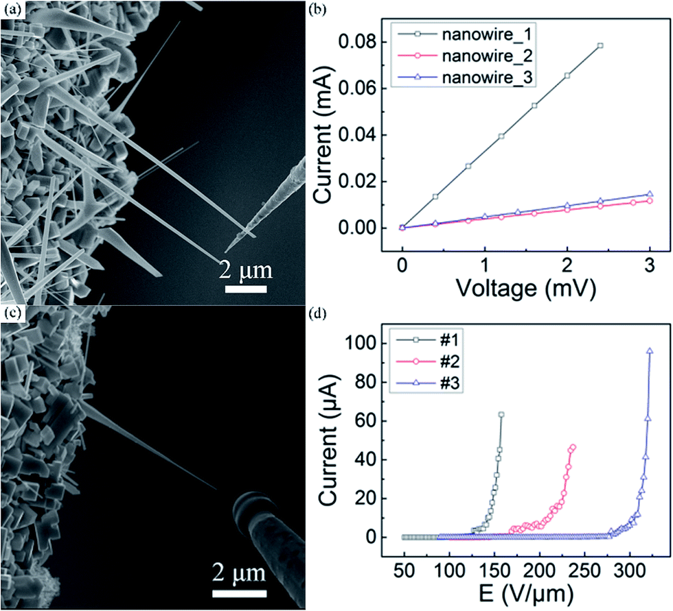 | ||
| Fig. 3 (a and c) The SEM images of an individual LaB6 nanowire during conductivity and FE measurements, respectively. (b and d) Typical I–V and FE curves of single LaB6 nanowires. | ||
FE measurements of the LaB6 nanowire film were carried out in our self-built FE analysis and measurement system, in which a flat metal sheet was used as the anode. The total area of the sample was about 0.3 cm2, and the distance between cathode nanowires and anode was kept at about 220 μm in all of the measurements. The chamber pressure was about 2 × 10⁻⁵ Pa. Representative J–E curve of the LaB6 nanowire film is given in Fig. 4(a). One can see that the turn-on and threshold fields of the LaB6 nanowires are respectively 2.2 V μm−1 (at 10 μA cm−2) and 2.9 V μm−1 (at 1 mA cm−2), which are low enough for practical applications in cold-cathode electron sources. The highest current of the LaB6 nanowire films can reach as high as 5.6 mA (16.7 mA cm−2) when the electric field is increased to 4.1 V μm−1. It is also found in Fig. 5(b) that the fluctuation at a very high emission current (5.2 mA) is only 1.7% in measurements lasting for 2 hours, which implies that the nanowire film possesses excellent emission stability. Based on the excellent emission performances of the LaB6 nanowires, they can meet the high-current requirements of cold-cathode electron sources.
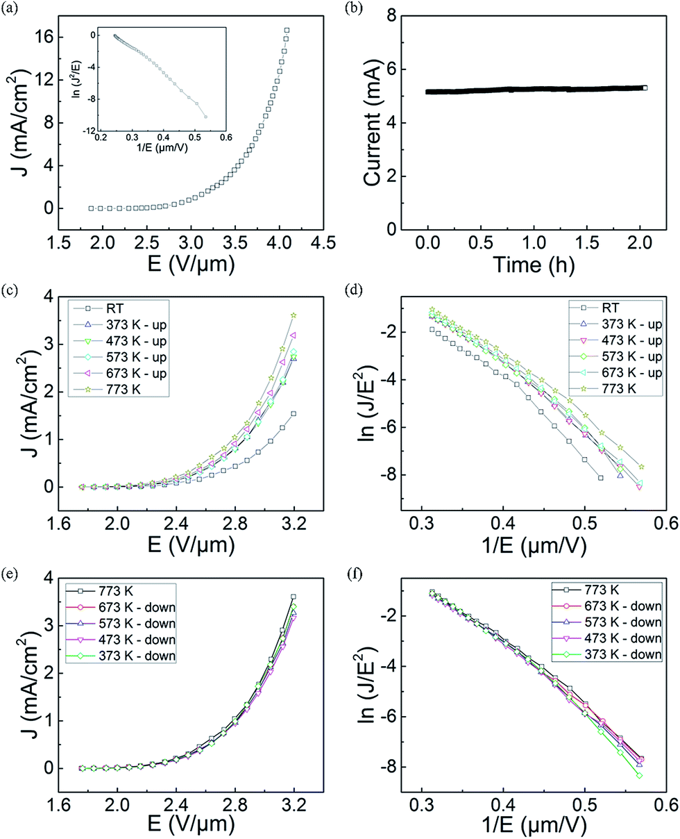 | ||
| Fig. 4 (a) Room-temperature J–E curves of the LaB6 nanowire film. The inset is their corresponding FN plots. (b) The FE stability curve of the LaB6 nanowires at room temperature. (c and d) The temperature-rising FE curves and FN plots of the LaB6 nanowires. (e and f) The temperature-dropping FE curves and FN plots of the LaB6 nanowires. | ||
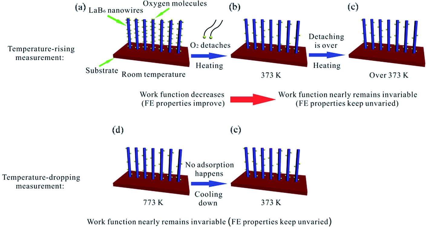 | ||
| Fig. 5 The diagram schematically illustrates the different emission performances of the LaB6 nanowires during temperature-rising and temperature-dropping FE measurements. | ||
For practical cold electron source applications, evaluating the temperature-dependent FE properties of the LaB6 nanowire film is very important. But up to now, there are a few groups investigating the effects of the temperature on the emission properties of the LaB6 nanowires.17,18 In these reports, the FE properties of the LaB6 nanowires are observed to be improved with the increase of temperature. But because the relevant experimental evidences are absent in these studies, it is hard to find out the intrinsic mechanisms for the temperature-dependent FE properties of LaB6 nanowires. Here, the FE measurements upon varied temperature are performed on the LaB6 nanowire film. The detailed experimental procedures are described as follows. Firstly, the sample is heated to over 773 K in an ultra-high vacuum chamber. Secondly, the sample is kept at 773 K for 1 hour to detach the adsorbed gas molecules on the surface of the nanowires. Finally, the FE properties are respectively recorded in a cycle of rising and reducing the temperatures. In this procedure, the whole FE measurements may last several days until all I–V curves exhibit the same change tendency at a given temperature to obtain enough accurate experimental data. Typical J–E curves and FN plots of the LaB6 nanowire film at temperature-rising process are indicated in Fig. 4(c) and (d), respectively. It is clearly seen in Fig. 4(c) that the FE behaviours of the LaB6 nanowires have been improved to some extent when the ambient temperature increases from room temperature to 773 K. The emission current density (3.61 mA cm−2) of the sample at 773 K is observed to be 2.3 times larger than that (1.54 mA cm−2) at room temperature at the same applied field of 3.2 V μm−1. But in the temperature-dropping measurements, the LaB6 nanowire film is seen to exhibit quite different variation tendency from that performed in temperature-rising measurements. As found in Fig. 4(e), the emission properties of the LaB6 nanowire film almost keep constant in the temperature-dropping measurements. To better compare their different variance tendency, Table 2 lists some important emission characteristics of the LaB6 nanowire film during temperature-rising and temperature-dropping measurements. In the whole temperature-dropping experiments, the turn-on and threshold fields of the sample are respectively 1.97 V μm−1 and 2.81 V μm−1. Moreover, their corresponding FN plots are seen to have a similar variance tendency and exhibit a slight deviation from the straight line at variable-temperature FE measurements. Generally, the space-charge effect30,31 or thermally-assisted emission32,33 effect is employed to illustrate the nonlinear behaviors of the FN plots. According to the space-charge model, high electric field can't timely remove the space charges from the surface of the nanowire and inhibit the electron emission to some extent, which results that the increase speed of the FE current at high fields turns slower than that at low fields. On the contrary, the increase of the FE current at high fields will become faster than that at low fields in the thermally-assisted emission model because larger emission current goes through the nanowires at high fields, which induces higher temperature occurs in the nanowires than that at low fields. Based on the FE behaviors of the LaB6 nanowires (Fig. 4), it can be concluded that rather than the thermal emission effect, the space charge effect should dominate over the emission process of the nanowire film.
| Temperature (K) | FE properties | ||||
|---|---|---|---|---|---|
| Turn-on field (V μm−1) | Threshold field (V μm−1) | Current density at 3.2 V μm−1 (mA cm−2) | Surface work function | ||
| Rising | RT | 2.13 | 3.05 | 1.54 | 2.96 |
| 373 | 2.03 | 2.86 | 2.69 | 2.87 | |
| 473 | 2.03 | 2.86 | 2.74 | 2.83 | |
| 573 | 2.00 | 2.86 | 2.85 | 2.78 | |
| 673 | 2.01 | 2.82 | 3.19 | 2.80 | |
| 773 | 1.94 | 2.78 | 3.61 | 2.67 | |
| Dropping | 673 | 1.94 | 2.80 | 3.4 | 2.67 |
| 573 | 1.98 | 2.81 | 3.27 | 2.75 | |
| 473 | 1.98 | 2.81 | 3.17 | 2.71 | |
| 373 | 1.98 | 2.80 | 3.4 | 2.77 | |
Because the FE performance of the LaB6 nanowires exhibit quite different variation tendency during the temperature-rising and temperature-dropping experiments, we try to explore the intrinsic temperature-dependent emission performances of the LaB6 nanowires to further evaluate their feasibility in applications of cold cathode electron sources. According to the classical FN theory,34,35 the effective work function and the field enhancement factor are two pivotal parameters for the emission properties of cathode materials. Because the field enhancement factor of the LaB6 nanowire film can be believed to keep invariable (1187) in the whole measurement range from room temperature to 773 K, the surface work function should be the key factor in determining their FE performances. It is known that the surface work function of the nanostructures is usually dependent on two factors, i.e., the ambient temperature and the content of gas molecules adsorbed onto the nanostructure surfaces. Generally, the work function of the LaB6 nanowires remains at 2.67 eV in the range from 300 K to 700 K based on previous study.2 But the surface work function of LaB6 is very sensitive to the gas molecules adsorbed onto the nanowire surfaces, especially for oxygen,36–38 which clearly differs from the temperature effect. So in our experiments, the FE properties of the LaB6 nanowires are likely determined by the oxygen content on the nanowires' surfaces, which is in good agreement with the explanations for the field emission process of α-Fe2O3 nanostructures.39 According to the above-mentioned analysis, we propose a possible mechanism to explain different FE performances of the LaB6 nanowires between temperature-rising and temperature-dropping measurements, as schematically illustrated in Fig. 5. Fig. 5(a)–(c) give the possible temperature-rising measurement process whereas the possible temperature-dropping measurement process are shown in Fig. 5(d) and (e). As seen in Fig. 5(b), the adsorbent oxygen molecules will gradually detach from the surface of the LaB6 nanowires when the temperature rises from room temperature to 373 K. Under this circumstance, the nanowires' surface work function becomes smaller with the successive desorption of oxygen molecules. It can be comprehensible that the desorption of oxygen gas will drive the La atoms to move much closer to the nanowire surfaces, which leads to the increase of the ionic surface dipole.40 As a result, the surface work function of LaB6 nanowires will decrease accordingly. Therefore, their turn-on and threshold fields correspondingly decrease, which is are in good agreement with initial temperature-rising results in Table 2. But if the temperature is continuously raised from 373 K to 773 K, the surface oxygen content nearly keeps unvaried because almost all of the oxygen molecules are already detached from the nanowires' surfaces except a little content of surface oxide residues generated by the initial heating treatment, as shown in Fig. 5(c). Correspondingly, the effective work function of the LaB6 nanowires nearly remains invariable in the subsequent temperature-rising measurements, which results that the turn-on and threshold fields of the sample are observed to be similar, as found in Fig. 4(c). In addition, more nanowires are activated with the proceeding of the measurement and involved in the FE process, which may be responsible for the slight improvement of their FE properties with the increase of temperature. But for the subsequent temperature-dropping measurements, the evolvement of the nanowire's work function is completely different from the temperature-rising measurements. Because the surface oxygen molecules have been eliminated from the ultra-high vacuum chamber in the temperature-rising process and no foreign oxygen gas can be supplied, oxygen molecules have no way to be attached onto the nanowire's surfaces in the temperature-dropping experiments, as explained in Fig. 5(e). In this situation, the oxygen content of the nanowires' surface still keeps unvaried in the temperature-dropping experiments (Fig. 5(e)), which will cause the invariance of their surface work function. Therefore, it is reasonable that FE performances of the LaB6 nanowire film during reduction of the temperature almost keep unvaried, as observed in Fig. 4(e) and (f).
To prove our above propositions, we designed two experiments, which are respectively the variable-temperature XPS measurements and the FE measurement of the LaB6 nanowires in oxygen ambient with different partial pressures. Fig. 6(a) gives the room-temperature XPS spectrum of the LaB6 nanowire film. As observed in Fig. 6(a), there are La, B, O, Si and C elements on the surface of the sample. The O peaks are found to be respectively located at 533.1 eV and 531.2 eV in high-resolution XPS spectrum (Fig. 6(c)). The peak at 533.1 eV may come from SiO2, boron oxide or oxygen molecules adsorbed on the boron atoms,41–43 and another peak at 531.2 eV results from the adsorbent oxygen on the La atoms.41,44 Hence, it can be confirmed that the oxygen molecules have been adsorbed onto the nanowire's surface, which is in good agreement with the EDX result shown in Fig. 2(d). Subsequently, the variable-temperature XPS measurements are performed on the same region of the sample, and the curve of the oxygen content versus the temperature is provided in Fig. 6(c) to further study the surface adsorption effect of the oxygen molecules. It is clearly seen that the oxygen concentration adsorbed onto the nanowire's surface will turn smaller with the increase of ambient temperature. When the temperature ranges from room temperature to 473 K, the concentration of the adsorbent oxygen has reduced to only 60% of room temperature concentration, which coincides with our above temperature-rising mechanism very well. It is also found that the oxygen content exhibits a slight increase with the temperature over 473 K. This slight increase can be attributed to the measurement errors of the XPS technique on the quantitatively analysis of the atom ratio inevitably exists in our experiments, which usually ranges from 0.5% to 1%. It can be understood that the oxygen content (4.92%) at 523 K can be considered as invariable in comparison with that (4.68%) at 473 K, which also conforms to our FE results (Fig. 4). So the XPS results reveal that our mechanism should be reasonable.
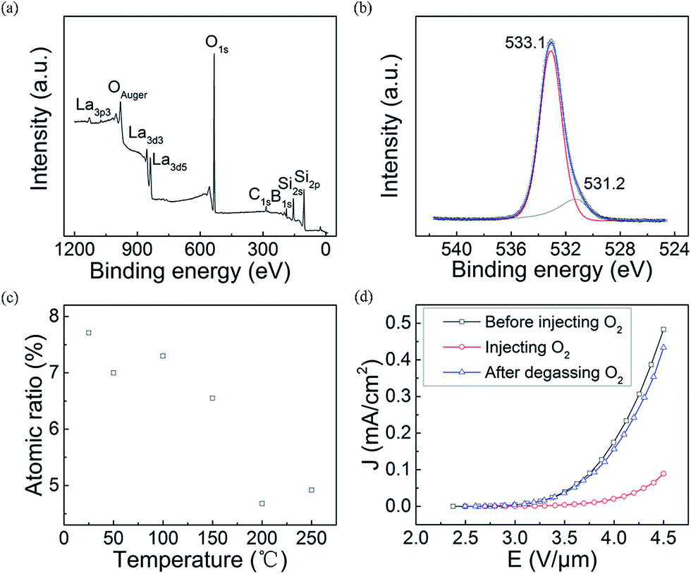 | ||
| Fig. 6 (a) A survey scan of LaB6 nanowire film; (b) XPS of O1s region of LaB6 nanowires. (c) The curve of the adsorbent oxygen content of LaB6 nanowires versus temperature; (d) FE curves of LaB6 nanowires at different oxygen contents. | ||
Meanwhile, FE properties of the LaB6 nanowire film in different oxygen atmosphere were compared together to simulate their emission performances in the aforementioned temperature-rising or temperature-dropping measurement process. Fig. 6(d) shows the J–E curves of LaB6 nanowires in different oxygen atmosphere. When a small amount of oxygen gas was fed into the vacuum chamber, the chamber pressure varied from about 1 × 10⁻⁵ Pa to 7.9 × 10⁻⁵ Pa. One can see that the turn-on field of LaB6 nanowires clearly increases from 3.2 V μm−1 to 3.8 V μm−1 with the introduction of the oxygen gas. It is also seen that the maximum emission current density (0.089 mA cm−2) of the sample after oxygen adsorption has decreased by 81.5% in comparison with it (0.48 mA cm−2) before oxygen adsorption at the same field of 4.5 V μm−1. It proves that the FE properties of the LaB6 nanowires after oxygen adsorption deteriorate to great extent compared with those before the adsorption, which also matches the temperature-rising results very well (Fig. 4(c)). It is noted that the FE properties of LaB6 nanowires can nearly recover (89.8%) to the original excellent performances after the oxygen molecules detaches from the nanowires' surfaces. This conforms to our temperature-dropping measurement results (Fig. 4(d)), which corroborates our mechanism again. Therefore, it comes to a conclusion that the oxygen content adsorbed onto the surfaces of the LaB6 nanowires plays a key role in determining their emission properties at variable temperatures. In addition, the recoverable emission characteristics of the LaB6 nanowires after desorbing the oxygen molecules suggest that they should have a long-term duration in air, which is very beneficial for their practical applications in power devices.
Conclusions
In this work, we have developed a moderate and low-cost method to fabricate single-crystal LaB6 nanowires on Si substrate. The LaB6 nanowires are indexed as single crystals with cubic structure, which grow along the [111] direction. In situ FE measurements show that individual LaB6 nanowires can bear the maximum current of 96.0 μA. The turn-on and threshold fields of the as-grown LaB6 nanowire film are respectively 2.2 V μm−1 and 2.9 V μm−1, which are low enough for cold cathode electron source applications. Their maximum current can reach as high as 5.6 mA (16.7 mA cm−2) at 4.1 V μm−1, which meets the high-current requirement of cold cathode electron sources. Meanwhile, the LaB6 nanowire film is found to exhibit quite different temperature-dependent FE properties in temperature-rising and temperature-dropping measurements, which should be attributed to the adsorption and desorption of the oxygen gas on the nanowire's surface. Considering that the LaB6 nanowires after O2 desorption still have recoverable FE performances comparable to other excellent cathode nanomaterials, they should have potential applications in cold cathode electron sources.Acknowledgements
The authors are very thankful for the support of the National Key Basic Research Program of China (grant No. 2013CB933601), National Project for the Development of Key Scientific Apparatus of China (2013YQ12034506), the Fundamental Research Funds for the Central Universities of China, the Science and Technology Department of Guangdong Province and the Education Department of Guangdong Province.References
- T. Tanaka, J. Phys. C: Solid State Phys., 1974, 7, 177–180 CrossRef.
- J. M. Lafferty, J. Appl. Phys., 1951, 22, 299 CrossRef CAS.
- P. A. Popov, V. V. Novikov, A. A. Sidorov and E. V. Maksimenko, Inorg. Mater., 2007, 43, 1187–1191 CrossRef CAS.
- S. Otani and Y. Ishizawa, J. Cryst. Growth, 1992, 118, 461–463 CrossRef CAS.
- K. Ebihara and S. Hiramatsu, Rev. Sci. Instrum., 1996, 67, 2765 CrossRef CAS.
- J. X. Qiu, B. Levush, J. Pasour, A. Katz, C. M. Armstrong, D. R. Whaley, J. Tucek, K. Kreischer and D. Gallagher, IEEE Microw. Mag., 2009, 10, 38–51 CrossRef.
- H. Makishima, H. Imura, M. Takahashi, H. Fukui and A. Okamoto, Int. Vac. Microelectron. Conf., Tech. Dig., 10th, 1997, 194–199 CAS.
- J. Tucek, D. Gallagher, K. Kreischer and R. Mihailovich, Int. Vac. Microelectron. Conf., 9th, 2008, 16–17 Search PubMed.
- H. Zhang, J. Tang, J. Yuan, Y. Yamauchi, T. T. Suzuki, N. Shinya, K. Nakajima and L. C. Qin, Nat. Nanotechnol., 2016, 11, 273–279 CrossRef CAS PubMed.
- H. Zhang, Q. Zhang, J. Tang and L. C. Qin, J. Am. Chem. Soc., 2005, 127, 2862–2863 CrossRef CAS PubMed.
- J. Q. Xu, Y. M. Zhao and C. Y. Zou, Chem. Phys. Lett., 2006, 423, 138–142 CrossRef CAS.
- D. J. Late, M. A. More, D. S. Joag, P. Misra, B. N. Singh and L. M. Kukreja, Appl. Phys. Lett., 2006, 89, 123510 CrossRef.
- J. R. Brewer, N. Deo, Y. Morris Wang and C. L. Cheung, Chem. Mater., 2007, 19, 6379–6381 CrossRef CAS.
- D. J. Late, K. S. Date, M. A. More, P. Misra, B. N. Singh, L. M. Kukreja, C. V. Dharmadhikari and D. S. Joag, Nanotechnology, 2008, 19, 265605 CrossRef PubMed.
- D. J. Late, M. A. More, S. Sinha, K. Dasgupta, P. Misra, B. N. Singh, L. M. Kukreja, S. V. Bhoraskar and D. S. Joag, Appl. Phys. A, 2011, 104, 677–685 CrossRef CAS.
- Q. H. Fan, Y. M. Zhao and D. D. Li, Ceram. Int., 2013, 39, 6271–6275 CrossRef CAS.
- J. Q. Xu, Y. M. Zhao and Q. Y. Zhang, J. Appl. Phys., 2008, 104, 124306 CrossRef.
- J. Q. Xu, G. H. Hou, H. Q. Li, T. Y. Zhai, B. P. Dong, H. L. Yan, Y. R. Wang, B. H. Yu, Y. Bando and D. Golberg, NPG Asia Mater., 2013, 5, e53 CrossRef CAS.
- F. Liu, J. F. Tian, L. H. Bao, T. Z. Yang, C. M. Shen, X. Y. Lai, Z. M. Xiao, W. G. Xie, S. Z. Deng, J. Chen, J. C. She, N. S. Xu and H. J. Gao, Adv. Mater., 2008, 20, 2609–2615 CrossRef CAS.
- F. Liu, H. B. Gan, D. M. Tang, Y. Z. Cao, X. S. Mo, J. Chen, S. Z. Deng, N. S. Xu, D. Golberg and Y. Bando, Small, 2014, 10, 685–693 CrossRef CAS PubMed.
- F. Liu, D. M. Tang, H. B. Gan, X. S. Mo, J. Chen, S. Z. Deng, N. S. Xu, Y. Bando and D. Golberg, ACS Nano, 2013, 7, 10112–10120 CrossRef CAS PubMed.
- P. Teredesai, D. V. S. Muthu, N. Chandrabhas, S. Meenakshi, V. Vijayakumar, P. Modak, R. S. Rao, B. K. Godwal, S. K. Sikka and A. K. Sood, Solid State Commun., 2004, 129, 791–796 CrossRef CAS.
- N. Ogita, S. Nagai, N. Okamoto, F. Iga, S. Kunii, J. Akimitsu and M. Udagawa, Phys. B, 2003, 328, 131–134 CrossRef CAS.
- N. Ogita, S. Nagai, N. Okamoto, M. Udagawa, F. Iga, M. Sera, J. Akimitsu and S. Kunii, Phys. Rev. B: Condens. Matter Mater. Phys., 2003, 68, 224305 CrossRef.
- F. Liu, C. M. Shen, Z. J. Su, X. L. Ding, S. Z. Deng, J. Chen, N. S. Xu and H. J. Gao, J. Mater. Chem., 2010, 20, 2197 RSC.
- Y. Shen, N. S. Xu, S. Z. Deng, Y. Zhang, F. Liu and J. Chen, Nanoscale, 2014, 6, 4659–4668 RSC.
- H. Zhang, J. Tang, Q. Zhang, G. P. Zhao, G. Yang, J. Zhang, O. Zhou and L. C. Qin, Adv. Mater., 2006, 18, 87–91 CrossRef CAS.
- Z. Xu, X. D. Bai, E. G. Wang and Z. L. Wang, Appl. Phys. Lett., 2005, 87, 163106 CrossRef.
- E. Minoux, O. Groening, K. B. Teo, S. H. Dalal, L. Gangloff, J. P. Schnell, L. Hudanski, I. Y. Bu, P. Vincent, P. Legagneux, G. A. Amaratunga and W. I. Milne, Nano Lett., 2005, 5, 2135–2138 CrossRef CAS PubMed.
- J. P. Barbour, W. W. Dolan, J. K. Trolan, E. E. Martin and W. P. Dyke, Phys. Rev., 1953, 92, 45–51 CrossRef.
- Y. Chen, S. Z. Deng, N. S. Xu, J. Chen, X. C. Ma and E. G. Wang, Mater. Sci. Eng., A, 2002, 327, 16–19 CrossRef.
- E. L. Murphy and R. H. Good, Phys. Rev., 1956, 102, 1464–1473 CrossRef CAS.
- Y. Z. Liu, Z. C. Wang and Y. Q. Dong, Electron Emission and Optoelectronic Cathodes, Beijing Institute of Technology Press, 1995, ch. 2, pp. 109–125 Search PubMed.
- R. H. Fowler and L. Nordheim, Proc. R. Soc. London, Ser. A, 1928, 119, 173–181 CrossRef CAS.
- H. Tomaschke and D. Alpert, J. Appl. Phys., 1967, 38, 881–883 CrossRef.
- M. Trenary, Sci. Technol. Adv. Mater., 2012, 13, 023002 CrossRef PubMed.
- R. Nishitani, S. Kawai, H. Iwasaki, S. Nakamura, M. Aono and T. Tanaka, Surf. Sci., 1980, 92, 191–200 CrossRef CAS.
- R. Nishitani, C. Oshima, M. Aono, T. Tanaka, S. Kawai, H. Iwasaki and S. Nakamura, Surf. Sci., 1982, 115, 48–60 CrossRef CAS.
- J. P. Lu, T. Yun, M. R. Zheng and S. C. Haur, J. Phys. Chem. C, 2011, 115, 8816–8824 CAS.
- M. A. Uijttewaal, G. A. de Wijs and R. A. de Groot, J. Phys. Chem. B, 2006, 110, 18459–18465 CrossRef CAS PubMed.
- C. L. Perkins, M. Trenary, T. Tanaka and S. Otani, Surf. Sci., 1999, 423, L222–L228 CrossRef CAS.
- D. S. Jensen, S. S. Kanyal, N. Madaan, M. A. Vail, A. E. Dadson, M. H. Engelhard and M. R. Linford, Surf. Sci. Spectra, 2013, 20, 36–42 CrossRef.
- W. C. Foo, J. S. Ozcomert and M. Trenary, Surf. Sci., 1991, 255, 245–258 CrossRef CAS.
- L. Schlapbach, Solid State Commun., 1981, 38, 117–123 CrossRef CAS.
Footnote |
| † These authors contribute equally to this work. |
| This journal is © The Royal Society of Chemistry 2017 |