
 Open Access Article
 This Open Access Article is licensed under a
 Creative Commons Attribution 3.0 Unported Licence
Enhanced photoelectrochemical performance of tungsten oxide film by bifunctional Au nanoparticles†
Yueqi Kongab,
Honggang Sun*a,
Weiliu Fanb,
Li Wanga,
Hongkai Zhaob,
Xian Zhao*b and
Shengzhong Yuanc
aSchool of Mechanical, Electrical & Information Engineering, Shandong University, Weihai, 264209, China. E-mail: sunhg@sdu.edu.cn; Fax: +86-531-88364864; Tel: +86-531-88366330
bState Key Laboratory of Crystal Materials, Shandong University, Jinan, 250100, China. E-mail: zhaoxian@sdu.edu.cn
cSupercomputing Center, Shandong University, Weihai, 264509, China
First published on 7th March 2017
Abstract
In the present study, Au nanoparticles were used to improve the photoelectrochemical performance of tungsten oxide film. Our study indicated that the surface plasmon resonance (SPR) of the Au nanoparticles at about 560 nm wavelength extended the light adsorption of the WO3 film. Mott–Schottky measurements and theoretical calculations determined that an inner electric field is built at the Au/WO3 interface through electronic transfer from Au to WO3. The measured photocurrent density and quantum efficiency results indicated that the synergistic effect of SPR and the inner electric field improved the PEC performance of the Au/WO3 photoelectrodes. However, the load of Au nanoparticles should be carefully considered due to the introduction of the surface recombined centers. The present study provides a reasonable understanding of the effects of the Au nanoparticles on the PEC performance of the WO3 film.
1. Introduction
Photoelectrochemical (PEC) water splitting for hydrogen and oxygen production has been paid considerable attention as it is a promising technology to alleviate both the energy crisis and environmental issues.1–5 For the PEC system, the properties of photoelectrode materials play an important role on the system performance. In recent years, the photoelectrode consisting of nanostructured n-type transition metal oxide has attracted increasing research interest due to the advantages of chemical stability, efficient light absorption, and ease of fabrication.6–11 Herein, tungsten oxide (WO3) has been seen as a promising photoelectrode material for the PEC water oxidation system due to its 2.6–2.8 eV band gap and photostability in water.12–15 Furthermore, WO3 can also provide enough overpotential for the crucial half reaction of oxygen evolution due to its favorable valence position (which is approximately 3 V versus NHE). Recently, Ma and coworkers reported that a mesoporous WO3 photoanode with a dual oxygen and tungsten vacancies-containing overlayer could greatly enhance the PEC activity for water oxidation, which was attributed to alleviating charge recombination at the electrode/electrolyte interface.16 Wang's group successfully prepared WO3 nanoplate arrays on FTO glass substrates by tuning the hydrothermal conditions, which presented the highest photocurrent density for the bare WO3 photoanode without any cocatalysts or sacrificial reagents.17Nevertheless, WO3 still suffers from some inadequacies, such as the rapid electron–hole recombination, lower reducibility of conduction band electrons, and limited response in most of the visible light region. To overcome these issues, various endeavors have been applied by controlling the nanostructure, doping other elements, constructing heterojunction, and loading cocatalysts.18–22 Ding et al. prepared one-dimensional nanostructured WO3 by a flame vapor deposition process, which achieved a maximum IPCE efficiency of 45.8% at 410 nm through controlling the size of the WO3 nanostructure.12 Yang and coworkers used Fe-doping to enhance the PEC performance of the WO3 photoanode, suggesting that this enhancement was related to doping-enhanced charge carrier density.23 Bard's group demonstrated that the efficient heterojunction formed on the interface of the ZnWO4/WO3 composite induced an increased PEC activity for water oxidation under both UV and visible illumination.24 In general, noble metals (such as Pt, Au, etc.) and some metal oxides (such as IrO2, RuO2, etc.) can act as the water splitting cocatalysts to improve the PEC performance of semiconductor based materials.25–30 Pt is usually used as a suitable hydrogen evolution cocatalyst. Bao et al. obtained a considerably high quantum yield (about 60.34%) when 3–5 nm Pt nanocrystals were loaded as cocatalysts onto CdS.26 Yang et al. fabricated a HfO2 passivation layer on the WO3 surface using a dip-coating method, which improved the WO3 PEC performance by suppressing the interfacial recombination of electrons and holes. Among them, Au nanoparticles have been focused on and used to extend the light response region due to their surface plasmon resonance (SPR)31,32 when coupled with appropriate materials.33–35 TiO2 decorated by Au nanoparticles showed an enhanced PEC performance due to the increased optical absorption associated with the SPR effect. Wu's group noted that the Au nanoparticles in the CdS–Au–TiO2 system not only acted as a photosensitizer extending the light response wavelength from 525 to 725 nm but also promoted the interfacial charge transfer.33 Two effects of the loaded Au nanoparticles, both the surface catalysis and the optical functions, were also observed on the CeO2 surface to determine the final photocatalytic performance.36 Therefore, a positive role of the Au nanoparticles on the WO3 photoelectrode can be expected for improving the PEC performance.
Herein, we report a facile hydrothermal method for in situ preparing WO3 films, and successfully obtaining a series of Au modified WO3 photoanodes by an immersion–calcination method. We characterized the PEC performance for all the samples under both simulated sunlight and visible light irradiation. DFT calculations together with experimental studies were employed to determine the optimal loading amount of Au nanoparticles, which revealed that the enhanced PEC performance is attributed to the two effects of the loaded Au nanoparticles. Our study takes the bifunctional roles of Au nanoparticles into consideration simultaneously, and thus can provide a new insight in designing different metal–semiconductor systems for PEC water oxidation.
2. Experimental
2.1 Preparation of WO3 crystal seeds
All reagents were of analytical grade and used as received without further purification. The WO3 film was fabricated with pre-seeding. In a typical procedure, 3.299 g of Na2WO4·2H2O was dissolved in 50 mL deionized water, and the abovementioned solution was vigorously stirred for 10 min. Then, 30 mL of 3 M HCl solution was added until no more faint yellow precipitate was formed. The yellow precipitate was collected by centrifugation and washed with deionized water. After that, the precipitate was dissolved into 2 mL H2O2 solution to obtain a yellow transparent sol, which was used as the WO3 crystal seed precursor. The as-prepared WO3 crystal seed precursor was then spun coated onto fluorine-doped tin oxide (FTO) glasses (with a size of 3 × 3.3 cm2 and a resistance of 7 ohm), which were ultrasonically washed beforehand by deionized water, acetone, and isopropyl alcohol in sequence. Finally, all the spin coated substrates were calcined at 523 K for 1 h.2.2 Preparation of WO3 film
1.1547 g Na2WO4·2H2O and 2.0453 g NaCl were dissolved into 70 mL deionized water and the abovementioned solution was vigorously stirred for 10 min. Then, the pH value of the solution was adjusted to 1.70 by drop-wise adding of 3 M HCl solution under constant stirring. The as-prepared solution was transferred into a 100 mL Teflon-lined stainless-steel autoclave and was the precursor for WO3 film growth. The FTO glass substrate coated by WO3 crystal seeds was placed at an incline against the internal wall of the Teflon-lined stainless-steel autoclave, which was sealed and maintained at 413 K for 4 h. The as-prepared WO3 film was rinsed with deionized water and alcohol in sequence and dried at 333 K for 1 h. Then, the WO3 film was treated in atmosphere at 523 K for 2 h.2.3 Preparation of Au nanoparticles modified WO3 film
5 M HAuCl4 solutions were prepared with high purity water at room temperature, and then the pH value of the abovementioned HAuCl4 solution was adjusted to 4.5 with 5 M NaOH solution. The WO3 film prepared as 2.2 was immersed into the HAuCl4 solution (pH 4.5) to form [AuCl(OH)3]− complex on WO3 surface, followed by calcination at 523 K for 2 h to grow Au nanoparticles.37 For the purpose of obtaining a series of Au-decorated WO3 film samples with different loading amounts, the immersion time was increased from 15 min to 4 h. The as-prepared Au modified WO3 films are denoted as Au/WO3-X (X represents the immersing time) in this study.2.4 Characterization
Powder X-ray diffraction (XRD) patterns were obtained on a D8 Advanced X-ray diffractometer (Bruker Germany), using Cu Kα radiation at a scan rate of 0.02° 2θ s−1. Scanning electron microscopy (SEM) was carried out using an S-4800 field emission SEM (FESEM, Hitachi, Japan) with an accelerating voltage of 5 kV. High-resolution transmission electron microscopy (HRTEM) analysis was conducted with the use of a JEM 2100 microscope at an accelerating voltage of 200 kV. X-ray photoelectron spectroscopy (XPS) measurements were performed on an ESCALAB 250 spectrometer equipped with an Al Kα source. All the binding energies were referenced to the C1s peak at 284.8 eV of the surface adventitious carbon. Ultraviolet visible (UV-vis) diffuse reflectance spectra were recorded using a UV-vis spectrophotometer (Shimadzu UV-2550, Japan).2.5 Photoelectrochemical measurements
The photoelectrochemical measurements were carried out by a workstation with a standard three electrode system, in which three electrodes were composed of the as-prepared WO3 film (with and without Au nanoparticles) samples as the working electrode, a Pt foil as the counter electrode and Ag/AgCl (saturated KCl) as the reference electrode. The electrolyte was 0.5 M Na2SO4 aqueous solution, and it was bubbled with nitrogen for 30 min under vigorous stirring before measurement. A 300 W Xe lamp (PLS-SXE300C, Beijing Trusttech Co., Ltd) was employed as the light source, and it was equipped with band-pass or cut-off filters to provide the required light irradiation. The photocurrent density with light on and off was measured by I–t curves at open circuit potential. Mott–Schottky curves were measured with an AC potential frequency of 1 kHz under dark conditions. The electrochemical impedance spectroscopy (EIS) was measured in the frequency range from 105 to 10−1 Hz under simulated sunlight irradiation. Moreover, the incident-photon-to-current-conversion efficiency (IPCE) was performed in the same three-electrode system at a zero bias versus Ag/AgCl using an electrochemical workstation.3. Results and discussion
3.1 Material characterization
The crystalline phases of the as-prepared WO3 film were determined from the XRD patterns. The XRD pattern of the FTO substrate is given in Fig. 1a, which is assigned to tetragonal SnO2 (JCPDS no. 41-1445). Fig. 1b gives the XRD patterns of the WO3 film on the FTO substrate, in which the characteristic peaks are assigned to hexagonal WO3·0.33H2O (JCPDS no. 35-1001). As shown in Fig. 1c, no impurity peaks and phase changes were observed after treating the film at 523 K. The strengthened peaks of the WO3 film indicated that the high-temperature annealing improved the WO3 crystallinity. The Au/WO3-X samples were also characterized by XRD, as shown in the ESI (Fig. S1†). All samples presented negligible changes compared with the bare WO3 film, which we attributed to trace amounts of Au loading.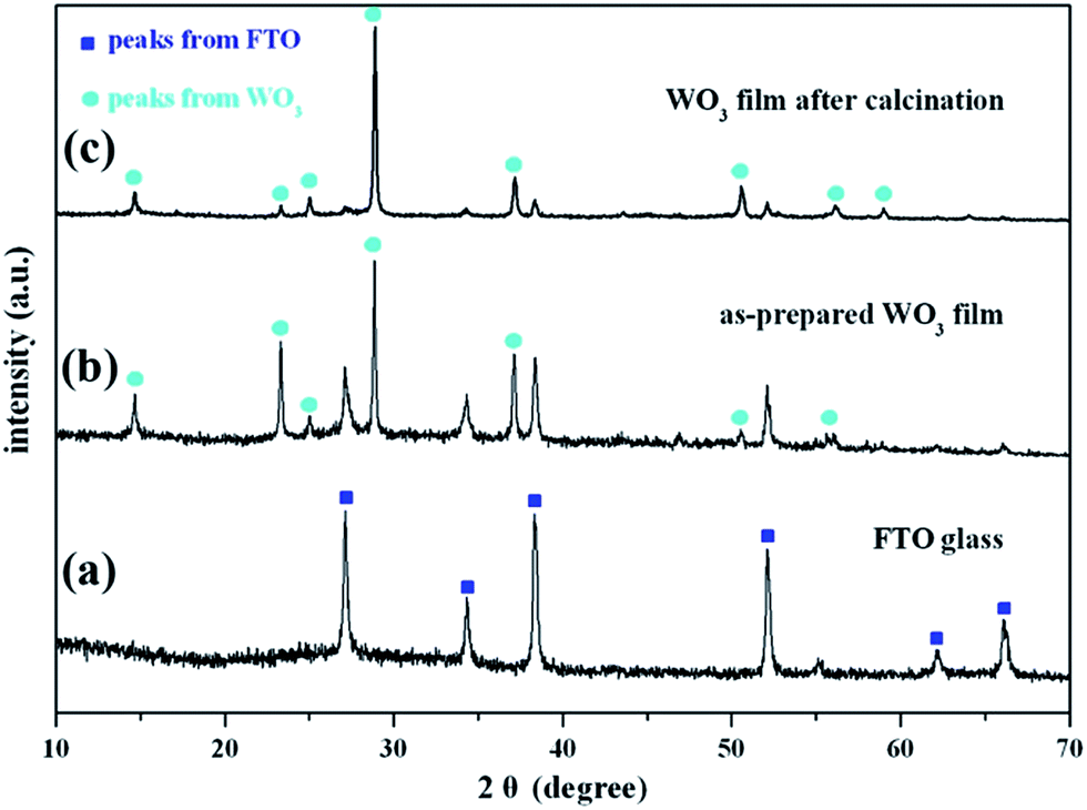 | ||
| Fig. 1 X-ray diffraction (XRD) patterns of (a) FTO substrate, as-prepared WO3 film samples (b) before and (c) after calcination at 523 K for 1 h in air. | ||
Fig. 2 shows the SEM of the as-prepared WO3 film before and after calcination at 523 K. As shown in Fig. 2a, the WO3 film mainly consisted of several block-like particles with 0.5–2 μm sizes after the hydrothermal process. Some nanorods were found to be dispersed on the substrate, which is consistent with the nanorods of the WO3 crystal seed layer. Fig. 2b shows that the particles mainly consisted of bundled nanorods with about 30 nm diameter. The nanorod-like WO3 morphology is in agreement with the previous results under the same experimental conditions.38 Fig. 2c and d present the morphology of the WO3 film after calcination, wherein more block-like particles on the substrate can be observed. Furthermore, as shown in Fig. 2e and f, the 560 nm thickness WO3 film with high-temperature treatment is much thicker than the 360 nm untreated film. The observation indicates that the high-temperature treatment promoted the growth and assembly of WO3 nanorods, which is in agreement with the improved WO3 film crystallinity from the XRD analysis.
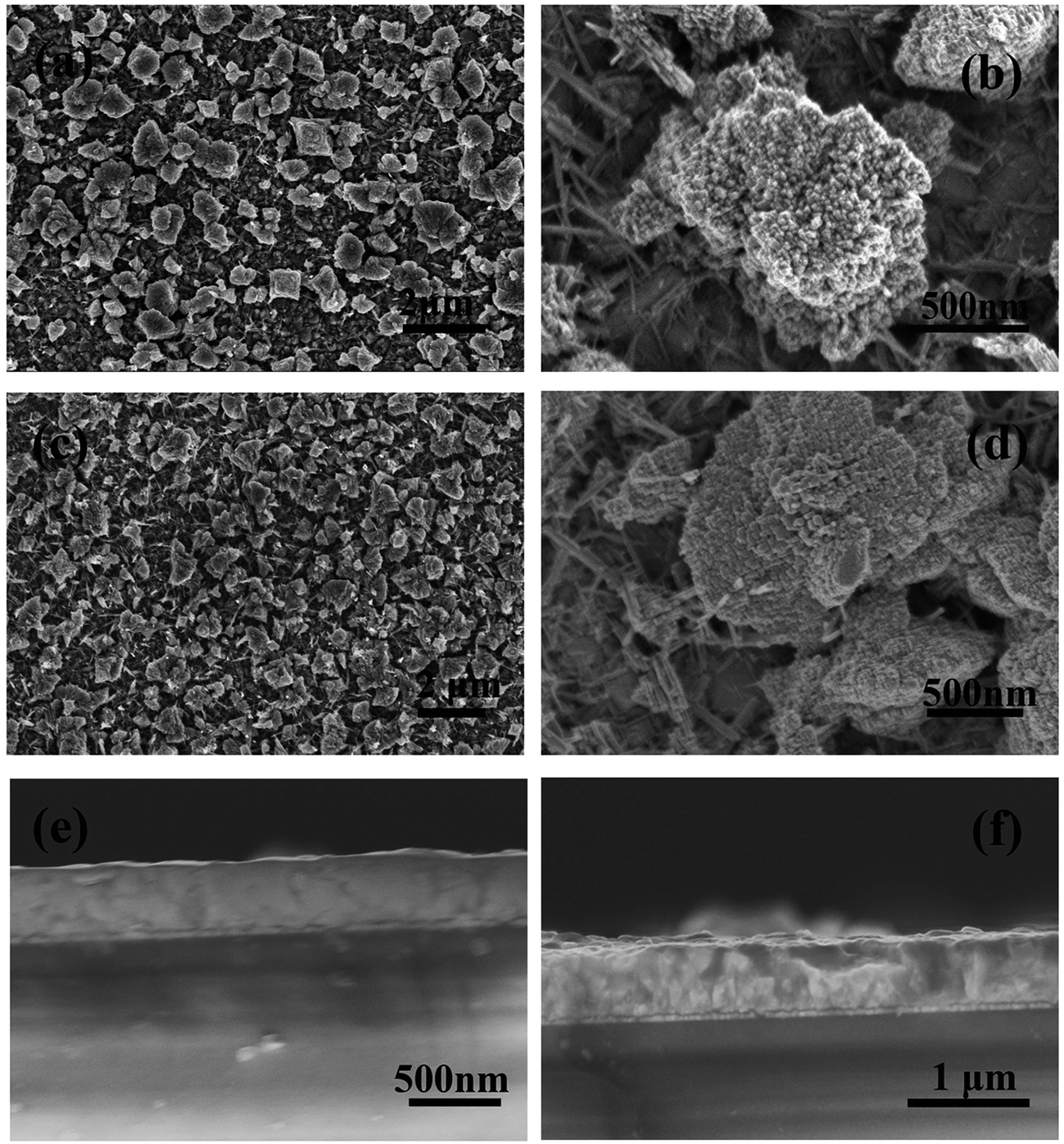 | ||
| Fig. 2 Top-view SEM images of WO3 film before (a and b) and after (c and d) calcination at 523 K, and cross-section SEM images of WO3 film before (e) and after (f) calcination at 523 K. | ||
Based on the abovementioned analysis, a three-stage growth technique of the WO3 film is proposed and illustrated in Fig. 3. First, peroxopolytungstic acid (PTA) is prepared by a sol–gel method, and then it is spin-coated onto the clean FTO substrate. The WO3 crystal seed layer with some tiny nanorods is formed by the decomposition of PTA under high-temperature treatment, as shown in Fig. S2.† Second, the crystal seed layer acts as nucleation sites for the WO3 particles to grow in the hydrothermal process. Over time, the initial nanorods gradually aggregate to form broccoli-like structures, and then the WO3 film is formed on the substrate. It is suggested that the precursor condition in the hydrothermal process plays an important role in the WO3 crystal phase and morphology.39 Third, WO3 nanorods further grow and aggregate by the high-temperature treatment. In the process, the continuation of the Ostwald ripening induces increased thickness and improved WO3 film crystallinity. The changes promote their electrical contact to the underlying FTO electrode.
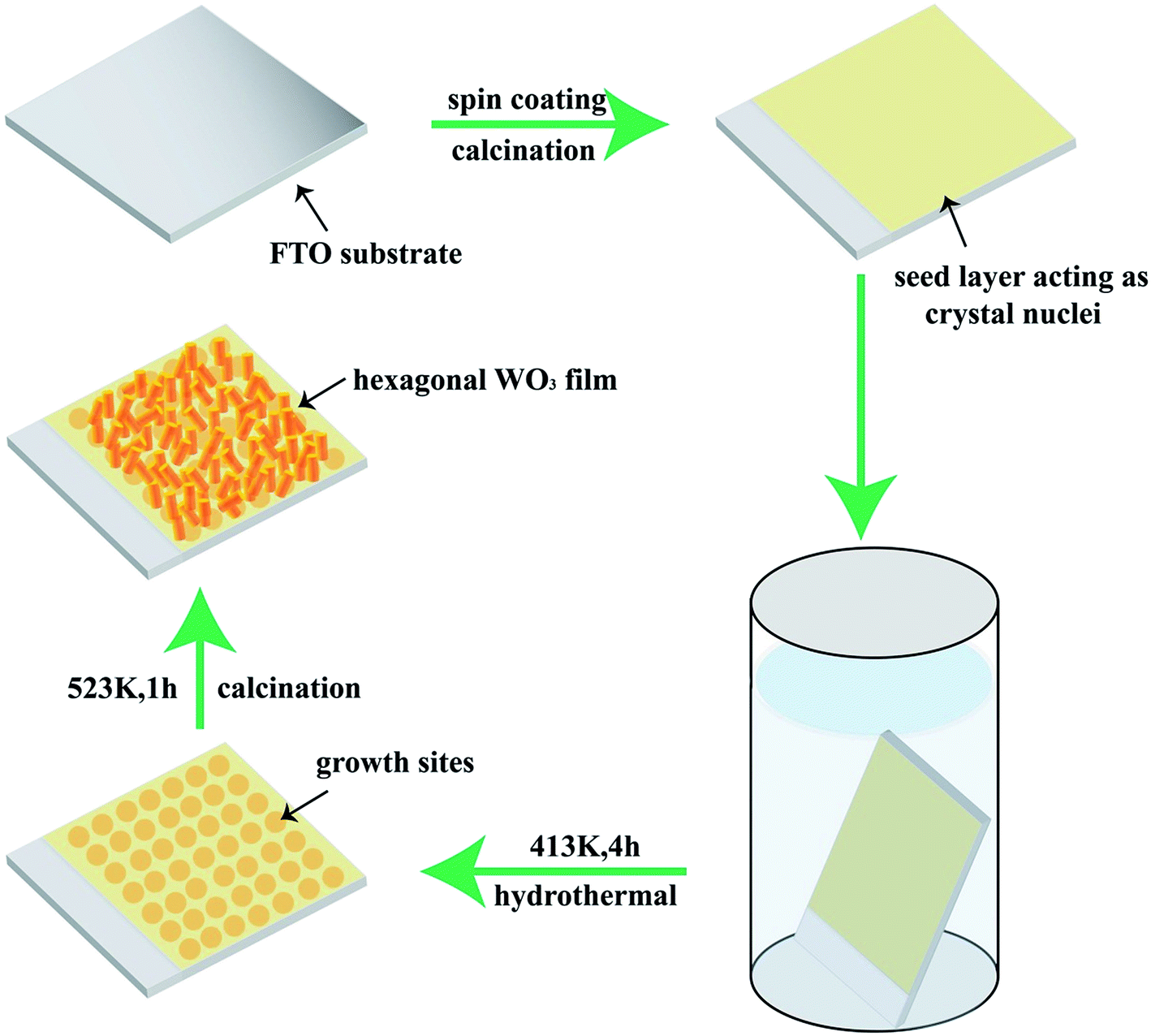 | ||
| Fig. 3 Schematic of the formation mechanism for the as-prepared WO3 film. | ||
The WO3 films are then immersed in the Au precursor solution, followed by calcination at 523 K to load Au nanoparticles. Fig. 4a and b give the SEM images of the Au/WO3-1 h sample, which show a similar morphology to the bare WO3 film. It should be noted that some nanoparticles were distributed on the WO3 film with 15–30 nm size. As shown in Fig. 4c and d, the HRTEM image taken at the interface of the nanoparticle and the WO3 nanorods clearly reveals two distinct sets of lattice fringes. The nanoparticle presented an interplanar spacing of 0.24 nm, which is indexed to the Au (111) plane. The interplanar spacing of 0.38 nm corresponds to the hexagonal WO3 (0001) plane, which indicates the 〈0001〉 growth orientation of the WO3 nanorod. The measured diameters of the Au nanoparticle and the WO3 nanorods were about 25 nm and 30 nm, respectively. In fact, no noticeable changes were observed for the size and shape of the Au nanoparticles with increased immersion time, as shown in Fig. S3,† which is in agreement with previous study.37 The good interface is in favor of the interaction between the Au nanoparticles and the WO3 nanorods.
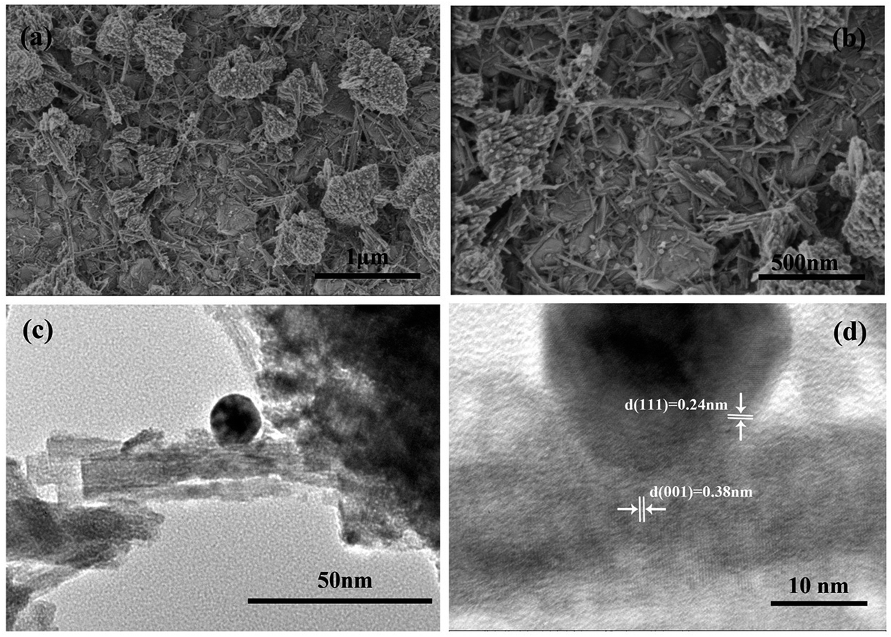 | ||
| Fig. 4 (a and b) SEM images and (c and d) HRTEM image for the Au/WO3-1 h sample. | ||
Fig. 5 gives the main surface chemical composition of the bare WO3 and Au/WO3-1 h films investigated by the XPS technique. As shown in Fig. 5a and b, the peaks have been divided into two different peaks (W4f5/2 and W4f7/2), and each W4f peak contains two oxidation states: W6+ with binding energies of 35.45 and 37.58 eV, and W5+ with binding energies of 34.90 and 37.05 eV.40,41 The calculated W5+/W6+ ratios are about 3.24% and 8.39% for the bare WO3 and Au/WO3-1 h films, respectively. Fig. 5c and d show the O1s core level spectra, in which the peak at 530.5 eV is ascribed to the lattice oxygen, while the peak at 532.0 eV is ascribed to oxygen vacancy and OH group adsorbed on the vacancy sites.42–44 Stronger vacancy states for the Au/WO3-1 h film were observed. Two reasons contribute to this observation: one is the interaction between Au nanoparticles and the surface oxygen of WO3, and the other is the remnant –OH from [AuCl(OH)3]− compound. The Au XPS spectrum, as shown in Fig. 5e, gives the characteristic peaks (Au4f5/2 and Au4f7/2). The peak with binding energy of 83.7 eV is attributed to Au0 states, and the peak with binding energy of 84.4 eV is attributed to Au+ states.41,45 The formation of Au+ states suggests that some holes were left at the Au/WO3 interface through the electronic transfer from Au to WO3. The process will influence the properties of the Au/WO3 photoelectrode, as discussed below. Moreover, the ratios of Au/W on the Au/WO3-X surfaces using XPS analysis are listed in Table 1, which shows an increasing Au amount as the immersion time is increased.
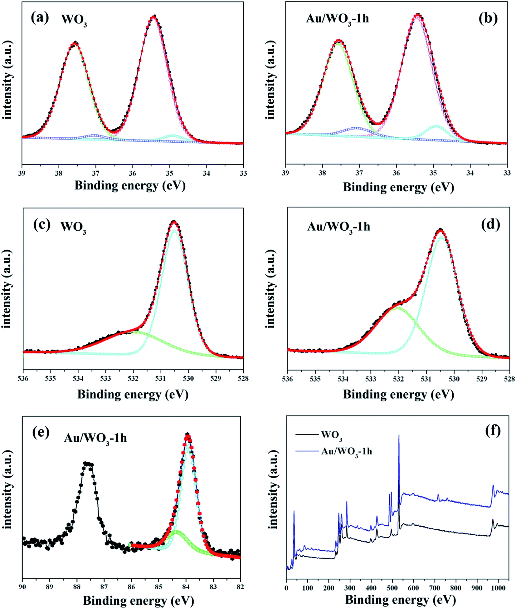 | ||
| Fig. 5 X-ray photoelectron spectra of region scans of (a and b) W4f, (c and d) O1s, (e) Au4f, and (f) the whole survey scans for the bare WO3 and Au/WO3-1 h samples. | ||
| Au/WO3-X | 0 | 15 min | 30 min | 1 h | 2 h | 4 h |
|---|---|---|---|---|---|---|
| Au/W (%) | — | 0.52 | 0.84 | 1.73 | 2.45 | 3.68 |
| W5+/W6+ (%) | 3.24 | 4.35 | 6.14 | 8.39 | 9.16 | 9.98 |
| Au+/Au (%) | — | 0.32 | 0.57 | 0.75 | 0.94 | 1.21 |
3.2 Photoelectrochemical performance
With the three-electrode system mentioned above, we studied the photocurrents of the WO3 photoelectrodes as a function of Au loading amount and compared them to those of the bare WO3 film. As shown in Fig. 6a and b, eliminating the effect of dark current, the simulated sun- and visible-light photocurrent densities of the bare WO3 film were about 5.1 and 0.02 μA cm−2, respectively. All the Au/WO3-X photoelectrodes showed a higher photocurrent density, as listed in Table 2. The results indicated that the loaded Au nanoparticles were favorable for improving the PEC performance. The Au/WO3-1 h photoelectrode presents the highest photocurrent densities of about 21.7 and 1.1 μA cm−2.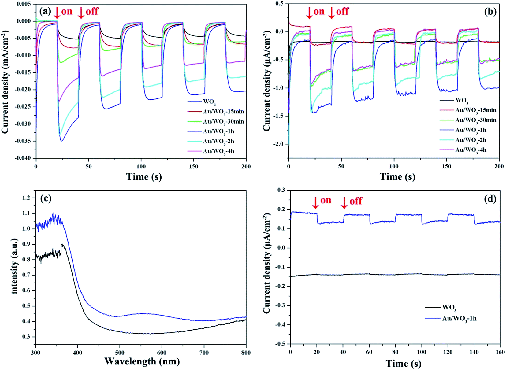 | ||
| Fig. 6 Photocurrent response of WO3 and Au/WO3-X samples (a) under simulated sunlight irradiation, and (b) under visible light (λ > 420 nm) irradiation. (c) UV-Vis diffuse reflectance spectra, and (d) photocurrent response with λ > 520 nm light irradiation of the bare WO3 and Au/WO3-1 h samples. | ||
| Au/WO3-X | 0 | 15 min | 30 min | 1 h | 2 h | 4 h | |
|---|---|---|---|---|---|---|---|
| Photocurrent densities (μA cm−2) | Sunlight | 5.1 | 6.6 | 6.7 | 21.7 | 16.5 | 12.2 |
| Visible light | 0.02 | 0.2 | 0.5 | 1.1 | 0.8 | 0.6 | |
| Vfb (eV) | 0.78 | 0.57 | 0.53 | 0.50 | 0.46 | 0.42 | |
| Rct (ohm) | 5537 | 5083 | 4521 | 2164 | 3661 | 5485 | |
| IPCE (%) | 350 nm | 10.81 | 19.14 | 24.83 | 35.79 | 26.99 | 21.67 |
| 420 nm | 0.39 | 1.07 | 2.07 | 3.51 | 1.57 | 1.16 | |
| 500 nm | 0.08 | 0.18 | 0.35 | 0.47 | 0.46 | 0.29 | |
Fig. 6c shows the UV-vis absorption spectra obtained from the WO3 films in the absence and presence of Au nanoparticles. The bare WO3 film displays an absorption edge at around 420 nm, which matches the band gap of hexagonal tungsten trioxide. The broad and weak absorption region beyond 700 nm is assigned to the effect of oxygen vacancy.46,47 Although there are almost no changes of the host absorption edge, the presence of Au nanoparticles loaded on the WO3 films extended the absorption range up to 700 nm. The absorption band centered at 560 nm corresponds to the surface plasmon resonance (SPR) of the Au nanoparticles. The SPR peak is correlated with the size, shape, and the surrounding environment of the Au nanoparticle.48 Although the center of the SPR peak of 10 nm Au nanospheres in an aqueous solution is typically at 520 nm, the SPR peak would redshift to 560 nm when the Au nanoparticles were deposited on the WO3 surface.49 The redshift was also observed in the Au/TiO2 system, where the size and shape of the Au nanoparticle are similar to those in the present study. As shown in Fig. 6d, the photocurrent density of the Au/WO3-1 h photoelectrode was about 0.05 μA cm−2 under the λ > 520 nm light irradiation.
The results provide that the SPR of the Au nanoparticle plays an important role in improving the PEC performance through harvesting more sunlight.
We next emphasized the shape changes of the photocurrent curve. As shown in Fig. 6a and b, the photocurrent densities of the bare WO3 photoelectrode increased over time during each circulation. This characteristic is attributed to the continuous accumulation of the photoexcited electrons on the surface of the electrode, which originates from the weak reducibility of the WO3 semiconductor.50 However, for the Au/WO3-X photoelectrodes, the photocurrent curves became square, and the steady-state photocurrents were quickly reached with increasing cyclic times, where the generating and consuming of the photoexcited electrons levelled off. The result implies that Au nanoparticles improved the reducibility of the WO3 semiconductor and promoted the reduction reactions on the electrode surface. In addition, a remarkable decay of the photocurrent curve was observed for the initial light-on stage in the Au/WO3-X photoelectrodes, and the effect was augmented with increasing Au amounts. The observation indicates that the electron–hole recombination process is present at the surface of photoelectrodes before achieving steady-state photocurrents.5 One of the reasons for the recombination is due to the reduction of the initially adsorbed O2 on the WO3 surface by the photoexcited electrons with improved reducibility; another reason should be the compensation of the initial holes accumulated at the Au/WO3 interface, as discussed with the XPS analysis. Therefore, although the SPR effect of the Au nanoparticles could expand the light response region of photoelectrodes, the modification should be carefully evaluated due to the losses of surface recombination.
In the present study, Mott–Schottky measurements for the bare WO3 and Au/WO3-X electrodes in the dark were conducted to investigate the influence of the Au nanoparticles on the WO3 electronic properties. As shown in Fig. 7a, all WO3 electrodes showed a positive slope in the Mott–Schottky plots, as expected for an n-type semiconductor. The flat band potential (Vfb) of the bare WO3 electrode was 0.26 eV versus Ag/AgCl. For the Au/WO3-X electrodes, this value was shifted to the negative direction. For comparison, the Vfb values were converted to go against a reversible hydrogen electrode (RHE) according to the Nernst equation51 as follows:
| ERHE (V) = EAg/AgCl + [0.059 (V) × pH] + E0Ag/AgCl (0.194 V) |
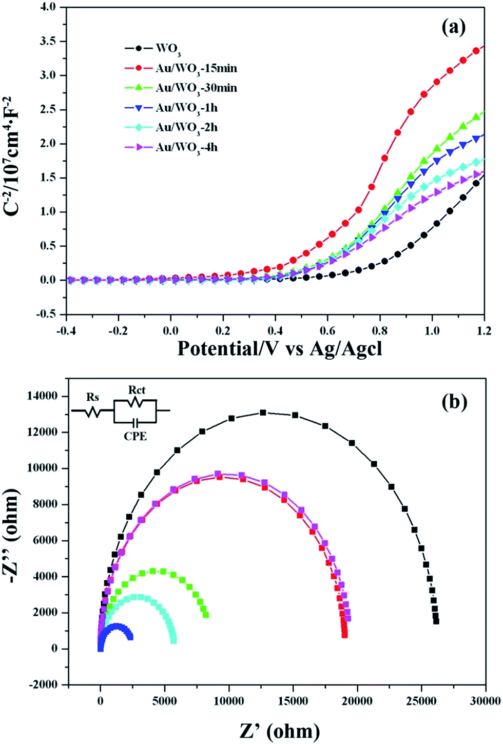 | ||
| Fig. 7 (a) Mott–Schottky plot and (b) electrochemical impedance spectroscopy Nyquist plots of WO3 and Au/WO3-X samples. | ||
The standardized flat band potentials were 0.78, 0.57, 0.53, 0.50, 0.46 and 0.42 eV for the bare WO3 and Au/WO3-X electrodes, respectively. The decreasing of the Vfb is related to the negative shift of the Fermi level of the electrodes, which is due to electronic accumulation on the WO3.52 DFT calculations were employed to analyze the electronic transfer process at the Au/WO3 interface. Fig. 8a and b present the optimized structures of the bare WO3 and Au/WO3 (010) surfaces. The two strong O–Au bonds were formed with 2.147 and 2.139 Å lengths, and the surface O–W bonds were elongated from 1.708 Å to 1.812 Å. The elongated bonds indicate that the surface O were activated by the adjacent Au, which agreed with the changes of O1s core level in the XPS analysis. Fig. 8c gives the electron density difference map at the Au/WO3 interface. It could be seen that some electrons of the Au are captured by the adjacent surface O ions, which causes a decrease in the work function of the WO3 surface from 7.32 eV to 6.90 eV. That is, the strong interaction of the Au and the surface O at the Au/WO3 interface is responsible for the negative shift of the Fermi level observed in the Mott–Schottky measurements. Importantly, the shift tendency with more Au loading was also observed by theoretical calculations, as shown in Fig. S4.† Therefore, we conclude that an inner electric field at the Au/WO3 interface with direction from Au to WO3 was built through the electron transfer process. The introduction of the inner electric field will promote the separation of the photoexcited electron–hole at the Au/WO3 interface, which is one of the reasons for the enhanced photocurrent density. To better understand the dynamics of electronic migration in the Au/WO3 photoelectrodes, the electrochemical impedance spectroscopy (EIS) measurements were conducted, and the results are shown in Fig. 7b. The semicircle in each Nyquist plot can be fitted using an equivalent circuit containing a series resistance (Rs), a charge transfer resistance (Rct) and a constant phase element (CPE). The EIS results gave a smaller charge transfer resistance (5083, 4521, 2164, 3661 and 5485 ohm) for the Au/WO3-X photoelectrodes compared with the 5537 for the bare WO3 photoelectrode. The result again confirms the present and effect of the inner electric field at the Au/WO3 interface. Note that further increasing the amount of Au nanoparticles did not further improve electronic transport in the Au/WO3-2 h and -4 h photoelectrodes. This characteristic is in accordance with the result of the photocurrents, which is attributed to the effect of the surface/interface recombination process induced by the Au nanoparticles.
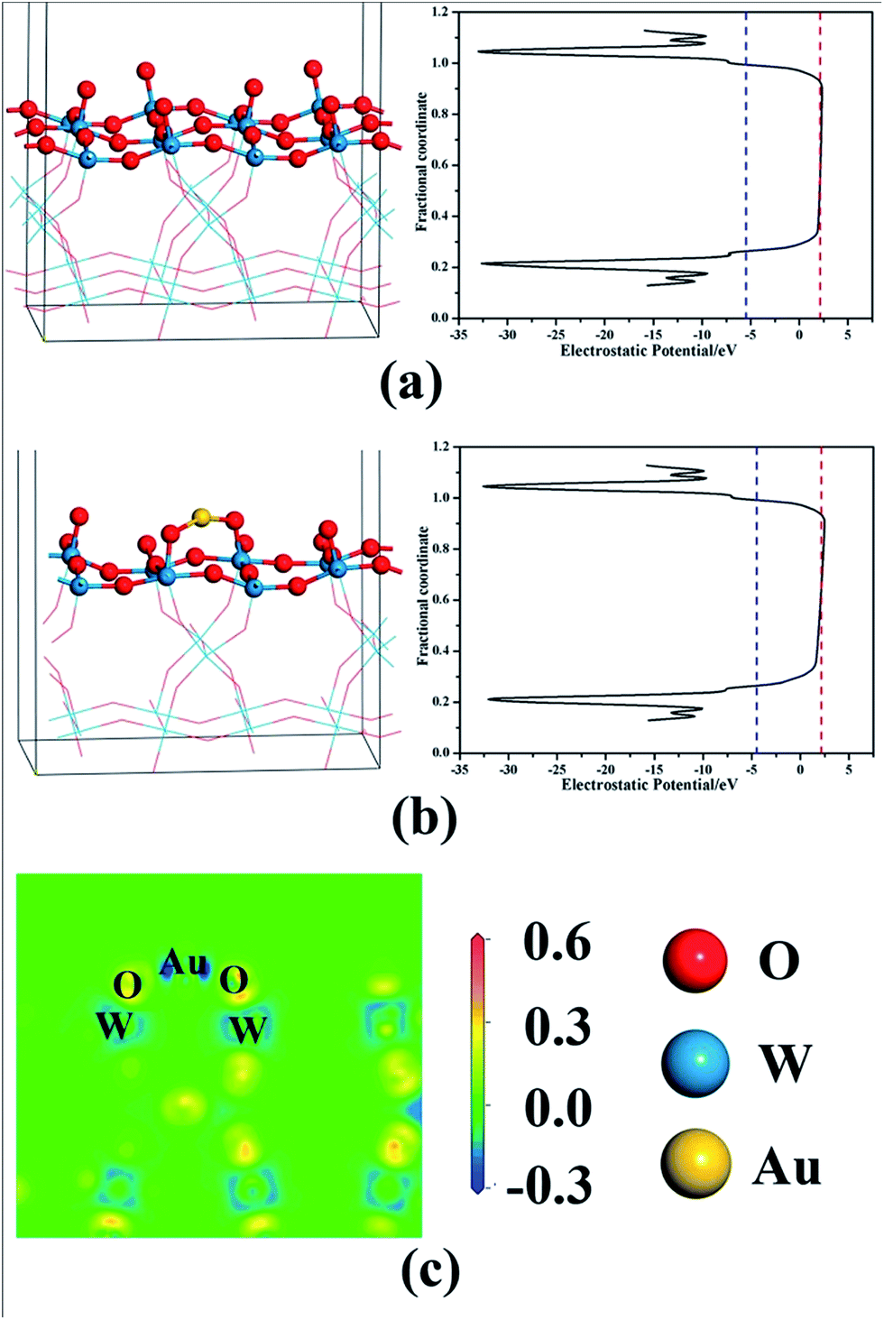 | ||
| Fig. 8 The structures and the potentials for (a) the bare WO3 and (b) the Au/WO3 surfaces, and (c) the electron different density map at the Au/WO3 interface. The blue and red dashed lines represent the Fermi and vacuum levels, respectively. | ||
The incident-photon-to-current-conversion efficiency (IPCE) spectra were collected to elucidate the contribution of the loaded Au nanoparticles. The IPCE values at specific wavelengths were calculated as follows:6
| IPCE = (1240I)/(λJlight) |
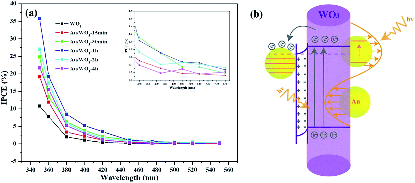 | ||
| Fig. 9 (a) IPCE plots of the WO3 and Au/WO3-X samples in 0.5 M Na2SO4 aqueous solution under illumination, and (b) proposed mechanism of the bifunctional Au nanoparticles under simulated sunlight irradiation. | ||
4. Conclusion
In the present study WO3 films were prepared by the hydrothermal method, and then the Au nanoparticles were loaded through an immersion method. The 10–20 nm Au nanoparticles showed a significant surface plasmon resonance, which induced the light adsorption at around 560 nm wavelength. The Mott–Schottky measurements and theoretical calculations indicated that an inner electric field is built at the Au/WO3 interface, which will promote separation of the photo-excited electron–hole pairs. The synergistic effect of SPR and the inner electric field improve the PEC performance of the Au/WO3 photoelectrodes. However, we also noted that the loading quantity for the Au nanoparticles should be carefully considered due to introduction of the recombined centers. The present study proposes bifunctional Au nanoparticles to improve the PEC performance of the WO3 photoelectrode, and provides a basic understanding to construct metal/semiconductor systems.Acknowledgements
This study is supported by the National Natural Science Foundation of China (Grant No. 51402169), and the Shandong Provincial Natural Science Foundation, China (Grant No. ZR2014BP005). The numerical calculations in this study were carried out on the supercomputing system in the Supercomputing Center, Shandong University, Weihai.References
- R. Abe, J. Photochem. Photobiol., C, 2010, 11, 179–209 CrossRef CAS.
- Y. J. Hwang, C. Hahn, B. Liu and P. D. Yang, ACS Nano, 2012, 6, 5060–5069 CrossRef CAS PubMed.
- L. Li, Y. Yu, F. Meng, Y. Tan, R. J. Hamers and S. Jin, Nano Lett., 2012, 12, 724–731 CrossRef CAS PubMed.
- G. Wang, H. Wang, Y. Ling, Y. Tang, X. Yang, R. C. Fitzmorris, C. Wang, J. Z. Zhang and Y. Li, Nano Lett., 2011, 11, 3026–3033 CrossRef CAS PubMed.
- D. K. Zhong, S. Choi and D. R. Gamelin, J. Am. Chem. Soc., 2011, 133, 18370–18377 CrossRef CAS PubMed.
- M. G. Ahmed, T. A. Kandiel, A. Y. Ahmed, I. Kretschmer, F. Rashwan and D. Bahnemann, J. Phys. Chem. C, 2015, 119, 5864–5871 CAS.
- M. Barroso, S. R. Pendlebury, A. J. Cowan and J. R. Durrant, Chem. Sci., 2013, 4, 2724 RSC.
- A. Kargar, Y. Jing, S. J. Kim, C. T. Riley, X. Q. Pan and D. L. Wang, ACS Nano, 2013, 7, 11112–11120 CrossRef CAS PubMed.
- M. T. Mayer, C. Du and D. Wang, J. Am. Chem. Soc., 2012, 134, 12406–12409 CrossRef CAS PubMed.
- K. Sivula, F. Le Formal and M. Gratzel, ChemSusChem, 2011, 4, 432–449 CrossRef CAS PubMed.
- X. Y. Yang, A. Wolcott, G. M. Wang, A. Sobo, R. C. Fitzmorris, F. Qian, J. Z. Zhang and Y. Li, Nano Lett., 2009, 9, 2331–2336 CrossRef CAS PubMed.
- J.-R. Ding and K.-S. Kim, AIChE J., 2016, 62, 421–428 CrossRef CAS.
- H. Li, G. Shi, H. Wang, Q. Zhang and Y. Li, J. Mater. Chem. A, 2014, 2, 11305 CAS.
- J. Yang, W. Li, J. Li, D. Sun and Q. Chen, J. Mater. Chem., 2012, 22, 17744 RSC.
- Y. Yang, R. Xie, Y. Liu, J. Li and W. Li, Catalysts, 2015, 5, 2024–2038 CrossRef CAS.
- M. Ma, K. Zhang, P. Li, M. S. Jung, M. J. Jeong and J. H. Park, Angew. Chem., Int. Ed., 2016, 55, 11819–11823 CrossRef CAS PubMed.
- S. C. Wang, H. J. Chen, G. P. Gao, T. Butburee, M. Q. Lyu, S. Thaweesak, J. H. Yun, A. J. Du, G. Liu and L. Z. Wang, Nano Energy, 2016, 24, 94–102 CrossRef CAS.
- H. I. Kim, J. Kim, W. Kim and W. Choi, J. Phys. Chem. C, 2011, 115, 9797–9805 CAS.
- C. W. Lai, S. Sreekantan, E. Pei San and W. Krengvirat, Electrochim. Acta, 2012, 77, 128–136 CrossRef CAS.
- S. L. Liew, Z. Zhang, T. W. G. Goh, G. S. Subramanian, H. L. D. Seng, T. S. A. Hor, H. K. Luo and D. Z. Chi, Int. J. Hydrogen Energy, 2014, 39, 4291–4298 CrossRef CAS.
- Y. Y. Liu, Y. Li, W. Z. Li, S. Han and C. J. Liu, Appl. Surf. Sci., 2012, 258, 5038–5045 CrossRef CAS.
- T. Zhu, M. N. Chong and E. S. Chan, ChemSusChem, 2014, 7, 2974–2997 CrossRef CAS PubMed.
- T. Zhang, Z. Zhu, H. Chen, Y. Bai, S. Xiao, X. Zheng, Q. Xue and S. Yang, Nanoscale, 2015, 7, 2933–2940 RSC.
- K. C. Leonard, K. M. Nam, H. C. Lee, S. H. Kang, H. S. Park and A. J. Bard, J. Phys. Chem. C, 2013, 117, 15901–15910 CAS.
- X. B. Chen, S. H. Shen, L. J. Guo and S. S. Mao, Chem. Rev., 2010, 110, 6503–6570 CrossRef CAS PubMed.
- N. Bao, L. Shen, T. Takata and K. Domen, Chem. Mater., 2008, 20, 110–117 CrossRef CAS.
- S. S. K. Ma, K. Maeda, R. Abe and K. Domen, Energy Environ. Sci., 2012, 5, 8390–8397 CAS.
- K. Maeda and K. Domen, J. Phys. Chem. Lett., 2010, 1, 2655–2661 CrossRef CAS.
- M. Ni, M. K. H. Leung, D. Y. C. Leung and K. Sumathy, Renewable Sustainable Energy Rev., 2007, 11, 401–425 CrossRef CAS.
- J. H. Yang, D. G. Wang, H. X. Han and C. Li, Acc. Chem. Res., 2013, 46, 1900–1909 CrossRef CAS PubMed.
- D. B. Ingram and S. Linic, J. Am. Chem. Soc., 2011, 133, 5202–5205 CrossRef CAS PubMed.
- A. Primo, T. Marino, A. Corma, R. Molinari and H. Garcia, J. Am. Chem. Soc., 2011, 133, 6930–6933 CrossRef CAS PubMed.
- J. Li, S. K. Cushing, P. Zheng, T. Senty, F. Meng, A. D. Bristow, A. Manivannan and N. Wu, J. Am. Chem. Soc., 2014, 136, 8438–8449 CrossRef CAS PubMed.
- F. Xu, Y. Yao, D. Bai, R. Xu, J. Mei, D. Wu, Z. Gao and K. Jiang, J. Colloid Interface Sci., 2015, 458, 194–199 CrossRef CAS PubMed.
- J. Zhu, X. Huo, X. Liu and H. Ju, ACS Appl. Mater. Interfaces, 2016, 8, 341–349 CAS.
- J. H. Yang, H. J. Yan, X. L. Wang, F. Y. Wen, Z. J. Wang, D. Y. Fan, J. Y. Shi and C. Li, J. Catal., 2012, 290, 151–157 CrossRef CAS.
- Y. C. Pu, G. Wang, K. D. Chang, Y. Ling, Y. K. Lin, B. C. Fitzmorris, C. M. Liu, X. Lu, Y. Tong, J. Z. Zhang, Y. J. Hsu and Y. Li, Nano Lett., 2013, 13, 3817–3823 CrossRef CAS PubMed.
- Y. Kong, H. Sun, X. Zhao, B. Gao and W. Fan, Appl. Catal., A, 2015, 505, 447–455 CrossRef CAS.
- L. Wang, J. Zhan, W. Fan, G. Cui, H. Sun, L. Zhuo, X. Zhao and B. Tang, Chem. Commun., 2010, 46, 8833 RSC.
- R. Azimirad, O. Akhavan and A. Z. Moshfegh, J. Phys. Chem. C, 2009, 113, 13098–13102 CAS.
- N. Naseri, R. Azimirad, O. Akhavan and A. Z. Moshfegh, Thin Solid Films, 2010, 518, 2250–2257 CrossRef CAS.
- Y. Baek and K. Yong, J. Phys. Chem. C, 2007, 111, 1213–1218 CAS.
- F. Peng, L. F. Cai, H. Yu, H. J. Wang and J. Yang, J. Solid State Chem., 2008, 181, 130–136 CrossRef CAS.
- Y. Wang, C. X. Feng, M. Zhang, J. J. Yang and Z. J. Zhang, Appl. Catal., B, 2010, 100, 84–90 CrossRef CAS.
- N. Naseri, M. Amiri and A. Z. Moshfegh, J. Phys. D: Appl. Phys., 2010, 43, 105405–105413 CrossRef.
- D. D. Du, W. J. Li, S. S. Chen, T. J. Yan, J. M. You and D. S. Kong, New J. Chem., 2015, 39, 3129–3136 RSC.
- S. J. Hong, H. Jun, P. H. Borse and J. S. Lee, Int. J. Hydrogen Energy, 2009, 34, 3234–3242 CrossRef CAS.
- J. T. Li, S. K. Cushing, J. Bright, F. K. Meng, T. R. Senty, P. Zheng, A. D. Bristow and N. Q. Wu, ACS Catal., 2013, 3, 47–51 CrossRef CAS.
- Y. C. Pu, G. M. Wang, K. D. Chang, Y. C. Ling, Y. K. Lin, B. C. Fitzmorris, C. M. Liu, X. H. Lu, Y. X. Tong, J. Z. Zhang, Y. J. Hsu and Y. Li, Nano Lett., 2013, 13, 3817–3823 CrossRef CAS PubMed.
- Y. Liu, C. S. Xie, J. Li, T. Zou and D. W. Zeng, Appl. Catal., A, 2012, 433, 81–87 CrossRef.
- S. Ikeda, N. Sugiyama, B. Pal, G. Marci, L. Palmisano, H. Noguchi, K. Uosaki and B. Ohtani, Phys. Chem. Chem. Phys., 2001, 3, 267–273 RSC.
- V. Subramanian, E. E. Wolf and P. V. Kamat, J. Am. Chem. Soc., 2004, 126, 4943–4950 CrossRef CAS PubMed.
Footnote |
| † Electronic supplementary information (ESI) available: The XRD patterns of the Au/WO3-X samples, the top-view images of the bare FTO glass with and without crystal seed, the HRTEM of Au/WO3-2 h and Au/WO3-4 h samples, and the surface structures and potentials for the WO3 (010) faces with two, three and four Au atoms. See DOI: 10.1039/c7ra01426k |
| This journal is © The Royal Society of Chemistry 2017 |