
 Open Access Article
 This Open Access Article is licensed under a Creative Commons Attribution-Non Commercial 3.0 Unported Licence
Improving the stability of the perovskite solar cells by V2O5 modified transport layer film†
Zhiyong Liu *ac,
Tingwei Hea,
Huihui Wangb,
Xiaohui Songac,
Hairui Liuac,
Jien Yangc,
Kaikai Liuc and
Heng Mac
*ac,
Tingwei Hea,
Huihui Wangb,
Xiaohui Songac,
Hairui Liuac,
Jien Yangc,
Kaikai Liuc and
Heng Mac
aDepartment of Physics and Materials Science, Henan Normal University, Xinxiang 453007, China. E-mail: zyliu01@163.com
bCollege of Civil Engineering and Architecture, Jiaxing University, Zhejiang 314001, China
cHenan Key Laboratory of Photovoltaic Materials, Xinxiang 453007, China
First published on 27th March 2017
Abstract
This study describes a method for producing highly stable perovskite solar cells (PSCs). On the basis of conventional PSCs, a high-performance device was prepared using a vanadium pentoxide (V2O5) film to modify the poly(3,4-ethylene dioxy-thiophene)–poly(styrene sulfonate) (PEDOT:PSS) hole transport layer (HTL). The V2O5 modified layer prevents the acidic PEDOT:PSS film from etching the indium tin oxide (ITO) electrode and maintains the stability of the PSC structure. In addition, a 4,7-diphenyl-1,10-phenanthroline (Bphen) modified layer prevented the photoactive layer film from coming into direct contact with the Ag electrode to enhance the lifetime of the PSC stored in the air. In our study, a stable power conversion efficiency (PCE) of 15.49% was achieved using this method. Compared to the same type of devices, this type of device exhibited excellent performance and its stability was much higher than that of other device structures when stored in air. On modifying the transport layers to enhance the stability and longevity of the PSC, a method is provided for reference for further research.
1. Introduction
With the increasing demand for global energy, energy issues have become the primary problem restricting the economic development of countries with solar energy, a green sustainable energy source, becoming a widespread concern.1–3 Recently, organic–inorganic halide perovskite solar cells (PSCs) have attracted significant attention due to their various advantages, such as long charge carrier diffusion length,4,5 broad and strong light absorption,6–8 longer carrier lifetime,9,10 and bipolar transport properties.11,12 The first PSC was prepared in 2009 with a power conversion efficiency (PCE) of 3.84%,13 and it has achieved fruitful research results in just eight years.14–23 The certified PCE of PSCs has reached 22.11%.24 Although we have improved the PCE, we still need to confront the problems of improving the stability and lifetime of the cells. These problems are a major obstacle for PSCs used to generate economic and social benefits. Therefore, this study describes a preparation method used to improve the stability and lifetime of PSCs.Planar heterojunction (PHJ) PSCs have a much simpler device structure with the perovskite active layer sandwiched between a hole transport layer (HTL) and electron transport layer (ETL), which avoids the high temperature process and pore-filling problems that occur during the preparation of the metal oxide scaffold layer. PHJ PSCs have two typical architectures: one with the regular configuration (n–i–p, ETL/CH3NH3PbI3/HTL),25 the other with an inverted configuration (p–i–n, HTL/CH3NH3PbI3/ETL).26 Since significant amounts of charge carriers are generated near the transparent conductive oxide, the inverted p–i–n configuration is more beneficial for charge collection compared to the regular n–i–p type because of the asymmetric diffusion length of the holes and the electrons in perovskite.27 So the configuration of PSCs has been improved on the basis of the latter in our study. Poly(3,4-ethylene dioxy-thiophene)–poly(styrene sulfonate) (PEDOT:PSS) is commonly used as the HTL in inverted PHJ PSCs.28–31 However, the acidic PEDOT:PSS layer sandwiched between indium tin oxide (ITO) and perovskite can etch the ITO electrode and decompose the perovskite film, which damages the stability of the devices.32–35 Some other HTL materials, such as nickel oxide (NiOx),36–39 lead sulfide (PbS)40 and graphene oxide41 have been adopted as the alternatives to the acidic PEDOT:PSS layer. However, they exhibit lower PCEs compared to the devices based on PEDOT:PSS.42 Although vanadium pentoxide (V2O5) nanowires and V2O5 mixed with PEDOT:PSS have been used to prepare the PSC device,43–45 their preparation process is more complicated. In addition, the device displayed a relatively low efficiency and little discussion was made in terms of its stability. Phenyl-C61-butyric acid methyl ester (PCBM) is commonly used as the ETL in PHJ PSCs.46–49 However, PCBM spin-coated on a CH3NH3PbI3 film surface will result in the appearance of some pores, which will be detrimental to the ETL electron transporting properties.50
Herein, the configuration of the PSC devices prepared was glass/ITO/V2O5/PEDOT:PSS/CH3NH3PbI3/PCBM/4,7-diphenyl-1,10-phenanthroline (Bphen)/Ag. CH3NH3PbI3, a perovskite active layer, was prepared by dissolving CH3NH3I and PbCl2 into N,N-dimethylformamide (DMF) at a molar ratio of 3![[thin space (1/6-em)]](https://www.rsc.org/images/entities/char_2009.gif) :1.51–53 PEDOT:PSS and PCBM were used as HTL and ETL, respectively. ITO and Ag were used as the top and bottom electrodes, respectively. V2O5 and Bphen were used as in the modified HTLs and ETLs,54 respectively. The V2O5 film is sandwiched between ITO electrode and PEDOT:PSS film, resulting in modification of HTL, and the Bphen film is sandwiched between Ag electrode and PCBM film, resulting in modification of ETL. We added a V2O5 modified layer film to prevent the acidic PEDOT:PSS film from etching the ITO electrode to protect the structure of the PSCs. The stability and lifetime of the devices produced using this method have been improved significantly. On the other hand, the V2O5 film utilizes different refractive index characteristics of the adjacent films, so that the absorption of photons by the perovskite layer was increased, and the photoelectric conversion efficiency of the device was improved. Bphen is a well-known organic electron transport material with high conductivity and electron transport rate. On one hand, we spin-coated a Bphen film on the PCBM film to increase the coverage of the ETL (PCBM/Bphen film) and prevent the photoactive layer film from coming into direct contact with the Ag electrode. On the other hand, a dense HTL (V2O5/PEDOT:PSS film) will prevent the photoactive layer film from coming into direct contact with water and oxygen from the external environment, and it will maintain the stability of the device when the device is stored in the air.
:1.51–53 PEDOT:PSS and PCBM were used as HTL and ETL, respectively. ITO and Ag were used as the top and bottom electrodes, respectively. V2O5 and Bphen were used as in the modified HTLs and ETLs,54 respectively. The V2O5 film is sandwiched between ITO electrode and PEDOT:PSS film, resulting in modification of HTL, and the Bphen film is sandwiched between Ag electrode and PCBM film, resulting in modification of ETL. We added a V2O5 modified layer film to prevent the acidic PEDOT:PSS film from etching the ITO electrode to protect the structure of the PSCs. The stability and lifetime of the devices produced using this method have been improved significantly. On the other hand, the V2O5 film utilizes different refractive index characteristics of the adjacent films, so that the absorption of photons by the perovskite layer was increased, and the photoelectric conversion efficiency of the device was improved. Bphen is a well-known organic electron transport material with high conductivity and electron transport rate. On one hand, we spin-coated a Bphen film on the PCBM film to increase the coverage of the ETL (PCBM/Bphen film) and prevent the photoactive layer film from coming into direct contact with the Ag electrode. On the other hand, a dense HTL (V2O5/PEDOT:PSS film) will prevent the photoactive layer film from coming into direct contact with water and oxygen from the external environment, and it will maintain the stability of the device when the device is stored in the air.
To further understand the performance of this type of cell structure, we compared four types of devices comprising V2O5 and Bphen modified layer films, without the V2O5 and Bphen modified layer films, with only the V2O5 modified layer film and with only Bphen modified layer film. The best device performance was observed with the V2O5 and Bphen modified layer films compared to the other three types of cell devices, and a stable PCE of 15.49% was achieved. In our study, 72 identical PSC devices with the V2O5 and Bphen modified layer films have an average power conversion efficiency (PCEAVE) of 13.96%. More importantly, after being stored in air for 300 h under ambient conditions of light soaking, the unencapsulated PSC devices with V2O5 and Bphen modified layer films still have a PCE of 11.45%, with a fall of about 73.9%. When the PCE of the other three types of PSC devices significantly decreased, the PCE of even the worst-performing PSC device was about 11.0% after being stored under same ambient conditions for 300 h.
2. Experimental
2.1 Materials and preparation
Chlorobenzene (C6H5Cl), hydrogen iodide (HI), methylamine (CH3NH2) and V2O5 were purchased from Shanghai Chemical Industry Co. PEDOT:PSS was purchased from Heraeus (Germany). PbCl2 (99.999%) and N,N-dimethylformamide (DMF) (anhydrous, amine free; 99.9%) were purchased from Alfa-Aesar. PC61BM and Bphen were produced by Nichem Fine Technology Co., Ltd. (Taiwan). CH3NH3I was synthesized from CH3NH2 with HI according to a literature procedure.55 V2O5 aqueous solutions were prepared by dissolving V2O5 powder directly into deionized water with stirring for over 12 h in air at room temperature at an optimized concentration of 0.05 wt%. The CH3NH3PbI3 solutions were prepared by solubilizing CH3NH3I and PbCl2 in DMF at a molar ratio of 3:1 whilst agitating the compound in a glovebox filled with N2 at 60 °C for 12 h. The PCBM solutions were prepared by dissolving the PCBM powder in chlorobenzene and churning the mixture in a glovebox for 12 h at an optimized concentration of 20 mg mL−1. The Bphen solutions were prepared from lysing Bphen powder in ethanol and rabbling the admixture in a glovebox for 12 h at an optimized concentration of 0.5 mg mL−1.
2.2 Etching and cleaning of the ITO substrate
First, the bulk ITO glass (Fine Chemicals Industry Co., Gyeonggi-do, Korea, 10 Ω sq−1) was cut into rectangles with a size of 13 mm × 15 mm. Next, 12 mm-wide conductive tape was stuck to the middle of the short side of the glass, ensuring no bubbles were trapped under the tape. Then, Zn powder was spread on the rim of the glass not covered by conductive paste, and concentrated hydrochloric acid was dropped onto the Zn powder. With the Zn powder as a catalyst, the concentrated hydrochloric acid may corrode the ITO film not covered with the conductive paste. To remove the stains on the ITO substrate, the substrate was repeatedly scrubbed using a cotton ball with detergent. Later, the substrate was washed using ultrasound in an NaOH solution to neutralize the acid, which does not react with the solution, for 10 min. Then, the ITO substrates were cleaned twice with ultrasound in deionized water, ethanol and acetone sequentially for 10 min in order to remove the water-soluble and organic impurities on the substrate. After being washed, the substrate was dried in a dry box at 100 °C for 10 min and treated in UV-Ozone cleaner for 15 min.2.3 Fabrication of the device
We prepared PSCs comprising the V2O5 and Bphen modified layer films using the following method. First, the V2O5 film was easily deposited on the clean ITO substrates under ambient conditions because water and oxygen in the air have no effect on the growth of the film. An aqueous solution of V2O5 was spin-coated at 2000 rpm for 40 s on the clean ITO substrates and dried at 140 °C for 15 min. Then, a PEDOT:PSS solution was spin-coated on the V2O5 films at 4500 rpm for 40 s and then dried at 140 °C for 20 min under ambient conditions. For the perovskite layer film, a CH3NH3PbI3 solution was spin-coated onto the PEDOT:PSS HTL film at 4000 rpm for 40 s in a N2 glovebox. Then, these operations were repeated with spin coating the perovskite thin films once again. The annealing of the wet perovskite films was carried out following a typical gradient increased temperature method that can be seen elsewhere.56–58 The substrates were gradually heated from 30 to 100 °C at a ramp rate of 10 °C/10 min on a hot plate, and the perovskite layer films were dried at 100 °C for 100 min. After that, the PCBM solution was deposited by spin-coating at 4000 rpm for 40 s onto the perovskite layer film in a N2 glovebox. Then, a Bphen solution was deposited by spin-coating at 2000 rpm for 40 s and dried at 60 °C for 10 min in a N2 glove box. Finally, the substrates were transferred to a vacuum chamber for silver electrode evaporation. Silver film was thermally deposited onto the Bphen modified layer film under vacuum at 4.5 × 10⁻⁵ Pa via a shadow mask, defining a single device area of 5.725 mm2. Thus, we could obtain the completed PSC devices.We prepared PSCs with other three types of device structure using the following method. For the first PSC without the V2O5 and Bphen modified layer, PEDOT:PSS films were prepared directly on the ITO electrode and the PCBM films were prepared directly on the Ag electrode. For the second type of PSC with only the V2O5 modified layer, the PEDOT:PSS films were prepared directly on the ITO electrode. For the third type of PSC with only the Bphen modified layer, the PCBM films were prepared directly on the Ag electrode. The other preparation conditions and methods used for these three types of PSCs are the same as the original.
2.4 Characterization
The surface and section morphology were characterized using field emission scanning electron microscopy (FESEM, Quanta 200 FEG, FEI Co.). Energy dispersive spectroscopy (EDS) was carried out using an EDS device connected to FESEM. The crystalline phase and X-ray diffraction (XRD) patterns of the perovskite films were recorded on a Rigaku D/MAX-2400 diffractometer. Steady-state photoluminescence (PL) measurements were conducted using an Edinburgh FLS980 fluorescence spectrophotometer with an excitation at 470 nm. The current density–voltage (J–V) curves were measured (2400 Series Source Meter, Keithley Instruments) under simulated Air-Mass (AM) 1.5 sunlight at 100 mW cm−2 (Newport, Class AAA solar simulator, 94023A-U). The incident-photon-to-current efficiency (IPCE) measurements were performed using a system comprising a xenon lamp, a monochromator, a chopper and a lock-in amplifier combined with a calibrated silicon photodetector. Atomic force microscopy (AFM) images were collected on an Agilent 5500 SPM system (Agilent Technologies, USA). UV-Vis absorption measurements were carried out using a Shimadzu UV-2550 spectrometer. Ultraviolet photoelectron spectroscopy (UPS) and the work function (WF) of V2O5 films were measured using UPS (Riken Keiki).3. Results and discussion
In conventional organic–inorganic PSCs, the acidic PEDOT:PSS HTL film is spin-coated on the ITO electrode surface, which causes serious damage to the ITO film and the stability of the device.59–61 In this study, we added a V2O5 modified layer film between the ITO electrode and the PEDOT:PSS HTL film to prevent the acidic PEDOT:PSS film from etching the ITO electrode in the PSCs. In order to learn the effect of the interface modification on the V2O5 film, FESEM together with EDS and elemental mapping was performed on the ITO/V2O5 film (Fig. S1a–j†) and ITO electrode (Fig. S1g–k†). We found that the surface morphology of ITO/V2O5 substrate film (Fig. S1a†) was more smooth and uniform compared with that of the original ITO glass substrate (Fig. S1g†). In the EDS spectrum of the ITO/V2O5 film (Fig. S1b†), an additional and clear signal for element V in addition to the signals for common elements, such as O, In, Sn, Ca, Na, Mg and Si (possibly from ITO or glass), was obtained. Moreover, like the distribution of the other elements (Fig. S1c–e and i–k†) in the ITO glass, the distribution of V (Fig. S1f†) was extremely homogeneous throughout the entire ITO/V2O5 film. In addition, the uniform and smooth film layers could also be observed in the AFM images, as shown in Fig. 1a–c. The surface roughness (root-mean-square, RMS) values of the V2O5 film, PEDOT:PSS film and the V2O5/PEDOT:PSS composite film on the ITO electrode are ∼2.8 nm, ∼2.1 nm and ∼2.0 nm, respectively. From the images, we found that the PEDOT:PSS film and V2O5/PEDOT:PSS film were more flat compared with the V2O5 film, and they had a similar roughness. The roughness of the film has a great influence on the preparation of the device and a reduction in the surface roughness may be advantageous for the device characteristics. Fig. 2a–c presents the FESEM images of the CH3NH3PbI3 films after being annealed on the V2O5 film, pristine PEDOT:PSS film and V2O5/PEDOT:PSS composite film, respectively. A large gap can be seen in the perovskite thin films directly spin-coated on the V2O5 film (Fig. 2a). Fig. 2b and c show that the PEDOT:PSS film and V2O5/PEDOT:PSS composite film were flat with a similar surface morphology. This suggests that V2O5 film with large roughness seriously impedes the spin-coating and crystal growth of the perovskite films. However, the V2O5 film has little impact on the growth and crystallization of the PEDOT:PSS film, as well as the morphology of the perovskite films. In Fig. 2d, we show the XRD patterns of three types of perovskite films. The two strong peaks of the perovskite film can be found at 14.14° and 28.48°,62 which correspond to the (110)- and (220)-orthorhombic crystal peaks for the perovskite films in the XRD pattern. The two highest peaks can be seen in the two perovskite films based on the V2O5/PEDOT:PSS and PEDOT:PSS layers. We found the two lowest peaks in the perovskite films based on the V2O5 layer. When compared with the other two perovskite films, the V2O5/PEDOT:PSS/CH3NH3PbI3 film with the strongest peaks has the highest degree of crystallinity. | ||
| Fig. 1 3D AFM images of (a) ITO glass coated with V2O5 film, (b) ITO glass coated with pristine PEDOT:PSS film and (c) ITO glass coated with the V2O5/PEDOT:PSS composite film. | ||
 | ||
| Fig. 2 FESEM images of the CH3NH3PbI3 films after annealing on (a) V2O5 film, (b) pristine PEDOT:PSS film and (c) the V2O5/PEDOT:PSS composite film, respectively. (d) The XRD spectra of the CH3NH3PbI3 films after annealing on V2O5 film, pristine PEDOT:PSS film and the V2O5/PEDOT:PSS composite film. | ||
A schematic and cross-section FESEM image of the prepared device comprising the V2O5 and Bphen modified layer films are shown in Fig. 3a and b. We added the V2O5 film between the ITO electrode and PEDOT:PSS HTL film to modify the HTL film. It can be seen that a 15 nm thick V2O5 film layer perfectly covers the ITO electrode. Because the acidic PEDOT:PSS film is in direct contact with the ITO electrodes, the acidic PEDOT:PSS penetrates and damages the ITO film, thereby affecting the cell structure and subsequently deteriorating the stability of the device. V2O5 film, as a buffer layer, modified PEDOT:PSS HTL, protecting the ITO electrodes and preventing the acidic film from etching the ITO electrode; this enhanced the stability and lifetime of the PSC. V2O5 film can not only protect the ITO electrode, but can also promote the perovskite layer to absorb photons. Fig. 4a presents the working principle diagram of the PSCs. When the PSC devices are irradiated with sunlight, photons are absorbed by the perovskite layer film to produce excitons after going through the glass, ITO electrode and the HTL films. Then, the excitons can produce electron–hole pairs at the interfaces between the perovskite layer and two transport layers. Due to the long charge carrier diffusion length of the PSCs, most of the electrons and holes will not recombine. After that, the top electrode and bottom electrode of cell can collect them in the ETL and HTL, respectively. Fig. 4b presents a diagram showing the mechanism of reflection of the photons by the V2O5 films in PSCs. When the photons are absorbed by the perovskite layer, some of photons produce electron–hole pairs and other photons are reflected out, which weakens the absorption rate of photons. The V2O5 film utilizes the different refractive index characteristics of the adjacent films63,64 and the photons may be reflected back by the V2O5 film layer. Therefore, there will be more photons being absorbed by the perovskite layer film, which will contribute to improving the PCE of the PSCs. Fig. 4c presents the UV-vis absorption spectra of the stacked films comprising PEDOT:PSS/CH3NH3PbI3 with and without the V2O5 film. A stronger absorption of the stacked films with V2O5 film was observed in the wavelength range of 300–800 nm. PL was carried out on ITO/V2O5/CH3NH3PbI3, ITO/PEDOT:PSS/CH3NH3PbI3 and ITO/V2O5/PEDOT:PSS/CH3NH3PbI3 to examine the radiative and non-radiative recombination channels, in the materials, as well as the charge transfer between the absorber and transport materials. A strong PL quenching of the emission is evidence for the efficient charge transfer from the photoactive layer to the charge transport layer.65 The quenching of the PL emission by the ITO/V2O5/PEDOT:PSS/CH3NH3PbI3 layer can be clearly observed in Fig. 4d. This indicates that the V2O5 film plays an important role for quenching recombination channels of the electrons and holes in the PSC devices.
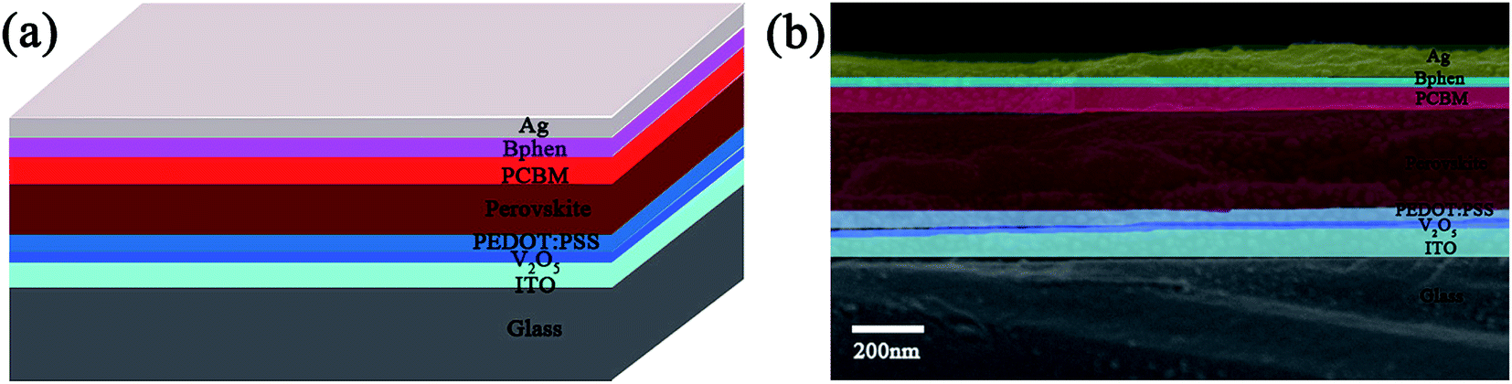 | ||
| Fig. 3 (a) A schematic and (b) cross-section FESEM image of the prepared device comprising the V2O5 and Bphen modified layer films. | ||
 | ||
| Fig. 4 (a) A schematic illustration of the working principle of the PSCs. (b) A schematic illustration of the mechanism in which the V2O5 film reflects photons. (c) The absorbance spectra of the perovskite layer film with the V2O5 film and without the V2O5 film. (d) The steady-state PL spectra of the V2O5/PEDOT:PSS/CH3NH3PbI3, PEDOT:PSS/CH3NH3PbI3 and V2O5/CH3NH3PbI3 layers deposited on ITO glass substrates (excited at 470 nm). | ||
Bphen is a well-known organic electron transport material with high electron mobility.66 It has been widely used as an ETL67 and a host material in the metal-doped electron-injecting layers68 used in organic light-emitting devices. As shown in Fig. 3a and b, we added a Bphen film between the PCBM ETL film and Ag electrode to play a role in modifying the ETL film. It can be seen that a 20 nm thick Bphen film layer perfectly covers the PCBM film. Fig. 5a and b show the FESEM surface images of CH3NH3PbI3/PCBM and CH3NH3PbI3/PCBM/Bphen stacked films. Gaps can be seen in Fig. 5a on the surface of the PCBM ETL film spin-coated on the perovskite layer film. When the Ag electrode is deposited on top of the device, it may come into contact with the perovskite layer, which is not covered completely by the PCBM film. In the absence of charge carrier transport, the electrons and holes will easily recombine and reduce the efficiency of the PSC. Adding a Bphen modified layer between the PCBM ETL and the Ag electrode covers the PCBM film completely and further improves the efficiency and lifetime of the PSC device (Fig. 5b). Some of the perovskite film was not covered by the PCBM film in the PSCs, which exposed the perovskite layer film to air. Perovskite thin films are very sensitive to water and oxygen in the air and are easily decomposed into PbI2, so that the perovskite film loses its ability to absorb photons. The Bphen modified layer on the PCBM film avoids the perovskite films from coming in direct contact with air to prevent the decomposition of the perovskite film, thus enhancing the stability and longevity of the device structure.
 | ||
| Fig. 5 FESEM surface images of the V2O5/PEDOT:PSS/CH3NH3PbI3/PCBM and V2O5/PEDOT:PSS/CH3NH3PbI3/PCBM/Bphen stacked films deposited on ITO glass substrates. | ||
By combining the V2O5 and Bphen modified layer films, PSCs with a structure of ITO/V2O5/PEDOT:PSS/MAPI/PCBM/Bphen/Ag were fabricated. Fig. 6a presents the J–V characteristics of the champion device under AM 1.5G illumination with a light intensity of 100 mW cm−2. A maximum PCE of 15.49% with a short circuit current density (JSC) of 22.88 mA cm−2, an open circuit voltage (VOC) of 0.94 V, and a fill factor (FF) of 0.73 was achieved. Fig. 6b presents the histograms of the PCE parameter in 72 cells. The range of the PCE was from 11% to 16%, with an average and minimum efficiency of 13.96% and 11.87%, respectively. All this suggests that the devices fabricated using this method show high reproducibility.
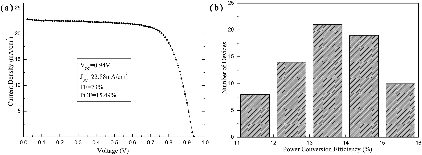 | ||
| Fig. 6 The performance and reproducibility of the PSCs. (a) J–V curve of the champion device with the V2O5 and Bphen modified layer films under AM 1.5G illumination with a light intensity of 100 mW cm−2. (b) A statistical histogram of the PCEs measured from 72 cells. | ||
In order to compare the performance of this device structure, various types of devices were compared comprising the V2O5 and Bphen modified layer films, without V2O5 and Bphen modified layer films, with only V2O5 modified layer film and with only Bphen modified layer film. Fig. 7a shows the IPCE spectra of the PSCs with the different structures. Compared to the device without the V2O5 and Bphen films, interestingly, there was an evident increase in the IPCE with a wide wavelength range in the PSCs with only the V2O5 film. Moreover, the device with V2O5 and Bphen films has a wider wavelength range and stronger absorption intensity. The wide band enhancement in the IPCE was attributed to the improved electrical properties of the V2O5 and Bphen modified transport layer films. Fig. 7b shows the J–V characteristics of the PSCs with different structures under AM 1.5G illumination with a light intensity of 100 mW cm−2. Table 1 shows the key performance parameters of the PSCs with the four different structures, including VOC, JSC, FF and PCE. There was a large effect of V2O5 and Bphen modified layer films on the device performance. The device with V2O5 and Bphen films demonstrated the best performance with a PCE of 15.49%, JSC of 22.88 mA cm−2, VOC of 0.94 V, and FF of 0.73. When compared to the device without the V2O5 and Bphen films, the JSC of the device with only the V2O5 film increased slightly from 19.26 mA cm−2 to 21.80 mA cm−2. For device with only the Bphen film, the VOC increased slightly from 0.86 V to 0.92 V, and the FF increased slightly from 0.64 to 0.71. Noticeably, the V2O5 and Bphen films have a greater impact on improving the JSC, VOC and FF of the PSC device. It is found that the JSC, VOC and FF in the device with the V2O5 and Bphen films increase when compared to that of the reference device. The JSC, VOC and FF improved largely from 19.26 mA cm−2 to 22.88 mA cm−2, from 0.86 V to 0.94 V and from 0.64 to 0.73, respectively. We attributed this to the good interface modification by the V2O5 and Bphen interfacial layer. The difference between the highest occupied molecular of the HTL and the lowest unoccupied molecule orbital of the ETL are reported to determine the upper limit of the VOC.69 UPS analysis was carried out to explore the WF of the V2O5 film. The UPS spectra of the V2O5 film are shown in Fig. S2.† The WF of V2O5 is 5.15 eV, which is 0.5 eV higher than that of PEDOT:PSS (WF of 5.10 eV).65 The higher VOC could be attributed to the higher WF of V2O5, leading to a potentially larger quasi-Fermi level splitting and a higher VOC. This WF change may not only lead to increased VOC but may enhance the extraction of the charge carriers from the absorption layer, and therefore reduce the carrier recombination.
 | ||
| Fig. 7 The (a) IPCE spectra and (b) J–V curves obtained for the PSCs with V2O5 and Bphen modified layer films without the V2O5 and Bphen modified layer films, with only the V2O5 modified layer film and with only the Bphen modified layer film. | ||
| Devices | VOC (V) | JSC (mA cm−2) | FF | PCE (%) |
|---|---|---|---|---|
| With V2O5 and Bphen | 0.94 (0.93 ± 0.02) | 22.88 (22.06 ± 0.82) | 0.73 | 15.49 (13.68 ± 1.81) |
| With only V2O5 | 0.89 (0.88 ± 0.02) | 21.80 (20.97 ± 0.91) | 0.64 | 12.85 (11.23 ± 1.65) |
| With only Bphen | 0.92 (0.91 ± 0.01) | 20.49 (19.77 ± 0.73) | 0.71 | 13.98 (12.45 ± 1.53) |
| None | 0.86 (0.85 ± 0.03) | 19.26 (18.41 ± 0.88) | 0.64 | 11.08 (9.22 ± 1.90) |
The stability of the devices is essential for the commercial application of PSCs. To investigate the effect of Bphen and V2O5 on the cell stability, degradation tests of the perovskite solar cells without encapsulation were carried out under identical storage conditions (in air, at room temperature with the humidity in the range of 25–30%). In addition, the stability measurements of the PSCs were conducted in accordance with the ISOS-L-1 standards.70 J–V measurements were made every 60 h under AM 1.5G illumination with a light intensity of 100 mW cm−2. Fig. 8a–d are the line charts showing the variation of the performance parameters of the four types of PSCs with time. Table 2 shows the changes in the PCE for the four types PSCs with time. In addition, Table S1† shows the key performance parameters of the PSCs with the four different structures after 300 h, including the VOC, JSC, FF and PCE. After 300 h, the PCE of the original device without V2O5 and Bphen modified layers is reduced from 11.08% to 1.22%, reducing down to ∼11.0% compared with initial PCE. However, PCE of the device with V2O5 and Bphen modified layers is reduced from 15.49% to 11.45% after 300 h, and reduced to ∼73.9% of the starting value. Moreover, the rate of decline in the efficiency of the devices with only the V2O5 film and with only the Bphen film was observed for the two types of devices. This directly indicates that the V2O5 and Bphen films play a significant role in maintaining the stability of the PSC devices. After 300 h, the VOC and FF of the device with Bphen film were not significantly reduced, while for the original device it was reduced quickly. This indicates that the perovskite layer film was protected under the Bphen modified layer film and cannot be in direct contact with air, and hence the perovskite layer film was not significantly damaged. Few of the electrons and holes generated recombine in light absorbing layer, significantly improving the stability of the PSCs devices. When compared with the original device, the JSC of the devices with the V2O5 film decreased slowly. This indicates that the V2O5 film effectively prevents the PEDOT:PSS HTL from coming into direct contact with the ITO electrode, protecting the integrity of the PSC structure and the stability of the devices. As known, PEDOT:PSS absorbs oxygen and water from air, which further penetrate to the subsequent layers to eventually reduce the device performance.71 Similarly, PCBM has a stability issue for PSCs due to the hydrophilicity of the ester group.72 In addition, perovskite is extremely sensitive to water in the air. If the perovskite film between PEDOT:PSS and PCBM films comes into contact with water from the air, it will be severely damaged. Herein, the V2O5 and Bphen films serve as protective layers, effectively blocking the passage of water from the air to the perovskite film. The improvement in the stability was achieved due to the simultaneous interfacial modification of the cathode and anode. Therefore, the stability of the device with the V2O5 and Bphen modified layer films is greatly improved when compared with that of the original device. The performance parameters for the four types of devices decrease rapidly in the previous 120 h and later decrease slowly. The devices exposed to the external environment are slightly damaged, and a more significant impact on the performance of the devices is observed initially. In the process used to measure the performance of the PSCs, the measurement probe slightly scratches the Ag electrode, leading to the destruction of device structure. By excluding these negative factors, we will be able to reflect the excellent performance of the devices through more accurate data.
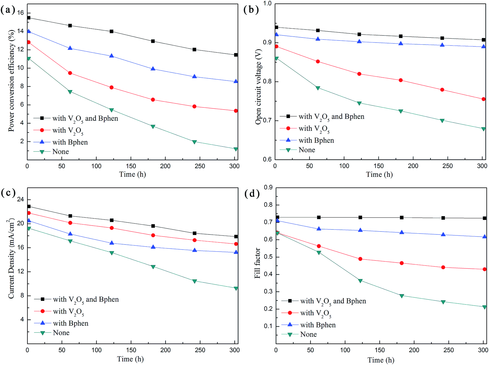 | ||
| Fig. 8 Line charts that show the variation in the performance parameter of the four kinds PSCs with time including the (a) PCE, (b) VOC, (c) JSC and (d) FF. | ||
| Devices | 0 h (%) | 60 h (%) | 120 h (%) | 180 h (%) | 240 h (%) | 300 h (%) |
|---|---|---|---|---|---|---|
| With V2O5 and Bphen | 100 | 94.48 | 90.42 | 83.53 | 77.64 | 73.92 |
| With only V2O5 | 100 | 73.84 | 61.61 | 51.23 | 45.49 | 41.76 |
| With only Bphen | 100 | 86.97 | 81.00 | 70.92 | 64.86 | 61.06 |
| None | 100 | 67.37 | 49.43 | 33.21 | 18.10 | 11.00 |
4. Conclusions
In summary, we demonstrated that the transport layers in planar PSCs can be modified using V2O5 and Bphen films, respectively. When compared with the reference PSC devices without V2O5 and Bphen films, the PCE of the best-performing PSC devices with the V2O5 and Bphen modified layer films was 15.49% and still maintained an efficiency of more than 70% after exposure to air. The V2O5 modified layer film increases the light absorption in the perovskite active layer by reflecting the photons. In addition, it prevents the acidic PEDOT:PSS film from etching the ITO electrode, thereby improving the stability of the cell structure. The Bphen modified layer film can cover the PCBM ETL film completely, preventing the Ag electrode from coming in direct contact with the perovskite layer, which extends the lifetime of the device. This indicates that the PSC devices comprising the V2O5 and Bphen films have more stable characteristics when compared with the devices with different structures. The results imply that the modified HTL and ETL provide a promising approach to improve the device configuration and enhance the device stability.Acknowledgements
The authors gratefully acknowledge the financial support from the Natural Science Foundation of China (NSFC Grant No. 51502081), the Doctoral Research Fund of Henan Normal University (No. 5101026500275, 5101029170256), the Science Funds for Young Scholar of Henan Normal University (No. 5101029279071), the Henan Province Programs for Science and Technology Development (Grant No. 122102210191), the Project of Basic and Advanced Technology Research of Henan Province of China (No. 122300410203), and the Basic Research Program of Education Bureau of Henan Province, China (No. 11A140014, 14A140010).Notes and references
- N. S. Lewis and D. G. Nocera, Proc. Natl. Acad. Sci. U. S. A., 2006, 103, 15729–15735 CrossRef CAS PubMed.
- G. W. Crabtree and N. S. Lewis, Phys. Today, 2007, 60, 37–42 CrossRef CAS.
- N. S. Lewis, Science, 2007, 315, 798–801 CrossRef CAS PubMed.
- J. M. Ball, M. M. Lee, A. Hey and H. J. Snaith, Energy Environ. Sci., 2013, 6, 1739–1743 CAS.
- C. W. Chen, H. W. Kang, S. Y. Hsiao, P. F. Yang, K. M. Chiang and H. W. Lin, Adv. Mater., 2014, 26, 6647–6652 CrossRef CAS PubMed.
- J. W. Cheng, S. T. Zheng and G. Y. Yang, Chem, 2007, 46, 10261–10267 CAS.
- S. Kazim, M. K. Nazeeruddin, M. Gratzel and S. Ahmad, Angew. Chem., Int. Ed., 2014, 126, 2854–2867 CrossRef.
- K. Wojciechowski, S. D. Stranks, A. Abate, G. Sadoughi, A. Sadhanala, N. Kopidakis, G. Rumbles, C. Z. Li, R. H. Friend and A. K. Y. Jen, ACS Nano, 2014, 8, 12701–12709 CrossRef CAS PubMed.
- S. D. Stranks, G. E. Eperon, G. Grancini, C. Menelaou, M. J. Alcocer, T. Leijtens, L. M. Herz, A. Petrozza and H. J. Snaith, Science, 2013, 342, 341–344 CrossRef CAS PubMed.
- C. Wehrenfennig, G. E. Eperon, M. B. Johnston, H. J. Snaith and L. M. Herz, Adv. Mater., 2014, 26, 1584–1589 CrossRef CAS PubMed.
- G. Xing, N. Mathews, S. Sun, S. S. Lim, Y. M. Lam, M. Grätzel, S. Mhaisalkar and T. C. Sum, Science, 2013, 342, 344–347 CrossRef CAS PubMed.
- M. Liu, M. B. Johnston and H. J. Snaith, Nature, 2013, 501, 395–398 CrossRef CAS PubMed.
- K. Akihiro, T. Kenjiro and S. Yasuo, J. Am. Chem. Soc., 2009, 131, 6050–6051 CrossRef PubMed.
- H. J. Snaith, J. Phys. Chem. Lett., 2013, 4, 3623–3630 CrossRef CAS.
- N. G. Park, J. Phys. Chem. Lett., 2013, 4, 2423–2429 CrossRef CAS.
- P. Gao, M. Grätzel and M. K. Nazeeruddin, Energy Environ. Sci., 2014, 7, 2448–2463 CAS.
- D. B. Mitzi, Prog. Inorg. Chem., 2007, 48, 1–121 CrossRef.
- T. C. Sum and N. Mathews, Energy Environ. Sci., 2004, 7, 2518–2534 RSC.
- J. H. Im, C. R. Lee, J. W. Lee, S. W. Park and N. G. Park, Nanoscale, 2011, 3, 4088–4093 RSC.
- H. S. Kim, C. R. Lee, J. H. Im, K. B. Lee, T. Moehl, A. Marchioro, S. J. Moon, R. Humphry-Baker, J. H. Yum, J. E. Moser, M. Gratzel and N. G. Park, Sci. Rep., 2012, 2, 591–597 Search PubMed.
- J. Burschka, N. Pellet, S. J. Moon, R. Humphry-Baker, P. Gao, M. K. Nazeeruddin and M. Gratzel, Nature, 2013, 499, 316–319 CrossRef CAS PubMed.
- H. Zhou, Q. Chen, G. Li, S. Luo, T. Song, H. S. Duan, Z. Hong, J. You, Y. Liu and H. Zhou, Science, 2014, 345, 542–546 CrossRef CAS PubMed.
- M. A. Green and T. Bein, Nat. Mater., 2015, 14, 559–561 CrossRef CAS PubMed.
- NREL, http://www.nrel.gov/ncpv/images/efficiency_chart.jpg, accessed 10 April 2016.
- F. Zuo, S. T. Williams, P. W. Liang, C. C. Chueh, C. Y. Liao and A. K. Y. Jen, Adv. Mater., 2014, 26, 6454–6460 CrossRef CAS PubMed.
- M. A. Green, A. Ho-Baillie and H. J. Snaith, Nat. Photonics, 2014, 8, 506–514 CrossRef CAS.
- J. H. Heo, H. J. Han, D. Kim, T. K. Ahn and S. H. Im, Energy Environ. Sci., 2015, 8, 1602–1608 CAS.
- J. Y. Jeng, Y. F. Chiang, M. H. Lee, S. R. Peng, T. F. Guo, P. Chen and T. C. Wen, Adv. Mater., 2013, 25, 3727–3732 CrossRef CAS PubMed.
- C. Zuo and L. Ding, Nanoscale, 2014, 6, 9935–9938 RSC.
- Z. Xiao, Q. Dong, C. Bi, Y. Shao, Y. Yuan and J. Huang, Adv. Mater., 2014, 26, 6503–6509 CrossRef CAS PubMed.
- J. Seo, S. Park, Y. C. Kim, N. J. Jeon, J. H. Noh, S. C. Yoon and S. I. Seok, Energy Environ. Sci., 2014, 7, 2642–2646 CAS.
- J. S. Yeo, R. Kang, S. Lee, Y. J. Jeon, N. Myoung, C. L. Lee, D. Y. Kim, J. M. Yun, Y. H. Seo, S. S. Kim and S. I. Na, Nano Energy, 2015, 12, 96–104 CrossRef CAS.
- M. P. De Jong, L. J. Van Ijzendoorn and M. J. A. De Voigt, Appl. Phys. Lett., 2000, 77, 2255–2257 CrossRef CAS.
- T. P. Nguyen and S. A. De Vos, Surf. Sci., 2004, 221, 330–339 CrossRef CAS.
- K. Norrman, M. V. Madsen, S. A. Gevorgyan and F. C. Krebs, J. Am. Chem. Soc., 2010, 132, 16883–16892 CrossRef CAS PubMed.
- J. H. Kim, P. W. Liang, S. T. Williams, N. Cho, C. C. Chueh, M. S. Glaz, D. S. Ginger and A. K. Y. Ken, Adv. Mater., 2015, 27, 695–701 CrossRef CAS PubMed.
- J. Y. Jeng, K. C. Chenk, T. Y. Chiang, P. Y. Lin, T. D. Tsai, Y. C. Chang, T. F. Guo, P. Chen, T. C. Wen and Y. J. Hsu, Adv. Mater., 2014, 26, 4107–4113 CrossRef CAS PubMed.
- J. Cui, F. Meng, H. Zhang, K. Cao, H. Yuan, Y. Cheng, F. Huang and M. Wang, ACS Appl. Mater. Interfaces, 2014, 6, 22862–22870 CAS.
- Z. Zhu, Y. Bai, T. Zhang, Z. Liu, X. Long, Z. Wei, Z. Wang, L. Zhang, J. Wang, F. Yan and S. Yang, Angew. Chem., Int. Ed., 2014, 53, 12571–12783 CAS.
- L. Hu, W. Wang, H. Liu, J. Peng, H. Cao, G. Shao, Z. Xie, W. Ma and J. Tang, J. Mater. Chem. A, 2015, 3, 515–518 CAS.
- Z. Wu, S. Bai, J. Xiang, Z. Yuan, Y. Yang, W. Cui, X. Gao, Z. Liu, Y. Jin and B. Sun, Nanoscale, 2014, 6, 10505–10510 RSC.
- J. You, Y. Yang, Z. Hong, T. B. Song, L. Meng, Y. Liu, C. Jiang, H. Zhou, W. H. Chang, G. Li and Y. Yang, Appl. Phys. Lett., 2014, 105, 183902–183906 CrossRef.
- J. Pan, P. Li, L. Cai, Y. Hu and Y. Zhang, Sol. Energy Mater. Sol. Cells, 2016, 144, 616–622 CrossRef CAS.
- C. X. Guo, K. Sun, J. Ouyang and X. Lu, Chem. Mater., 2015, 27, 5813–5819 CrossRef CAS.
- S. J. Lee, H. P. Kim, A. R. Bin Mohd Yusoff and J. Jang, Sol. Energy Mater. Sol. Cells, 2014, 120, 238–243 CrossRef CAS.
- Y. H. Lou, M. Li and Z. K. Wang, Appl. Phys. Lett., 2016, 108, 53301–53309 CrossRef.
- M. T. Dang, L. Hirsch and G. Wantz, Adv. Mater., 2011, 23, 3597–3602 CrossRef CAS PubMed.
- J. B. You, Z. R. Hong, Y. Yang, Q. Chen, M. Cai, T. B. Song, C. C. Chen, S. R. Lu, Y. S. Liu, H. P. Zhou and Y. Yang, ACS Nano, 2014, 8, 1674–1680 CrossRef CAS PubMed.
- J. H. Heo, H. J. Han, D. Kim, T. K. Ahn and S. H. Im, Energy Environ. Sci., 2015, 8, 1602–1608 CAS.
- Y. Bai, H. Yu, Z. Zhu, K. Jiang, T. Zhang, N. Zhao, S. Yang and H. Yang, J. Mater. Chem. A, 2015, 3, 9098–9102 CAS.
- S. Seo, I. J. Park, M. Kim, S. Lee, C. Bae, H. S. Jung, N. G. Park and H. Shin, Nanoscale, 2016, 8, 11403–11412 RSC.
- X. Gong, M. Li, X. B. Shi, H. Ma, Z. K. Wang and L. S. Liao, Adv. Funct. Mater., 2015, 25, 6671–6678 CrossRef CAS.
- Z. K. Wang, M. Li, D. X. Yuan, X. B. Shi, H. Ma and L. S. Liao, ACS Appl. Mater. Interfaces, 2015, 7, 9645–9653 CAS.
- M. Qian, M. Li, X. Shi, H. Ma, Z. K. Wang and L. S. Liao, J. Mater. Chem. A, 2015, 3, 13533–13539 CAS.
- M. M. Lee, J. Teuscher, T. Miyasaka, T. N. Murakami and H. J. Snaith, Science, 2012, 338, 643–647 CrossRef CAS PubMed.
- M. Saliba, T. K. Wee, S. Hiroaki, D. T. Moore, S. Trent, W. Zhang, L. A. Estroff, W. Ulrich and H. J. Snaith, J. Phys. Chem. C, 2014, 118, 17171–17177 CAS.
- H. L. Hsu, C. P. Chen, J. Y. Chang, Y. Y. Yu and Y. K. Shen, Nanoscale, 2014, 6, 10281–10288 RSC.
- S. Bai, Z. W. Wu, X. J. Wu, Y. Z. Jin, N. Zhao, Z. H. Chen, Q. Q. Mei, X. Wang, Z. Z. Ye and T. Song, Nano Res., 2014, 12, 1749–1758 CrossRef.
- M. P. D. Jong, L. J. V. Ijzendoorn and V. M. A. De, Appl. Phys. Lett., 2000, 77, 2255–2257 CrossRef.
- K. W. Wong, H. L. Yip, Y. Luo, K. Y. Wong, W. M. Lau, K. H. Low, H. F. Chow, Z. Q. Gao, W. L. Yeung and C. C. Chang, Appl. Phys. Lett., 2002, 80, 2788–2790 CrossRef CAS.
- V. Shrotriya, G. Li, Y. Yao, C. W. Chu and Y. Yang, Appl. Phys. Lett., 2006, 88, 73508–73515 CrossRef.
- Y. Xiao, G. Han, Y. Li, M. Li and J. Wu, J. Mater. Chem. A, 2014, 2, 16856–16862 CAS.
- H. Hoppe, N. S. Sariciftci and D. Meissner, Mol. Cryst. Liq. Cryst., 2002, 385, 113–119 CrossRef CAS.
- R. D. Shannon, R. C. Shannon, O. Medenbach and R. X. Fischer, J. Phys. Chem. Ref. Data, 2002, 31, 931–970 CrossRef CAS.
- H. T. Peng, W. H. Sun, Y. L. Li, S. Y. Ye, H. X. Rao, W. B. Yan, H. P. Zhou, Z. Q. Bian and C. H. Huang, Nano Res., 2016, 10, 1–12 Search PubMed.
- S. Naka, H. Okada, H. Onnagawa and T. Tsutsui, Appl. Phys. Lett., 2000, 76, 197–199 CrossRef CAS.
- H. Nakada, S. Kawami, K. Nagayama, Y. Yonemoto, R. Murayama, J. Funaki, T. Wakimoto and K. Imai, Polym. Prepr. (Am. Chem. Soc., Div. Polym. Chem.), 1994, 43, 2450–2451 Search PubMed.
- J. Kido and T. Matsumoto, Appl. Phys. Lett., 1998, 73, 2866–2868 CrossRef CAS.
- P. P. Boix, K. Nonomura, N. Mathews and S. G. Mhaisalkar, Mater. Today, 2014, 17, 16–23 CrossRef CAS.
- M. O. Reese, S. A. Gevorgyan, M. Jørgensen, E. Bundgaard, S. R. Kurtz and D. S. Ginley, et al., Sol. Energy Mater. Sol. Cells, 2011, 95, 1253–1267 CrossRef CAS.
- A. Kanwat and J. Jang, J. Mater. Chem. C, 2014, 2, 901–907 RSC.
- D. Zhao, Z. Zhu, M. Y. Kuo, C. C. Chueh and A. K. Y. Jen, Angew. Chem., Int. Ed., 2016, 55, 8999–9003 CrossRef CAS PubMed.
Footnote |
| † Electronic supplementary information (ESI) available. See DOI: 10.1039/c7ra01303e |
| This journal is © The Royal Society of Chemistry 2017 |