
 Open Access Article
 This Open Access Article is licensed under a Creative Commons Attribution-Non Commercial 3.0 Unported Licence
Annealing effects on the magnetic properties of highly-packed vertically-aligned nickel nanotubes
Vlad-Andrei Antohe *ab,
Emeline Nysten†
a,
Juan Manuel Martínez-Huerta‡
a,
Pedro Miguel Pereira de Sáa and
Luc Piraux*a
*ab,
Emeline Nysten†
a,
Juan Manuel Martínez-Huerta‡
a,
Pedro Miguel Pereira de Sáa and
Luc Piraux*a
aInstitute of Condensed Matter and Nanosciences (IMCN), Université Catholique de Louvain (UCL), B-1348 Louvain-la-Neuve, Belgium. E-mail: luc.piraux@uclouvain.be; Tel: +32 10 473 566
bResearch and Development Center for Materials and Electronic & Optoelectronic Devices (MDEO), Faculty of Physics, University of Bucharest, 077125 Bucharest-Măgurele, Romania. E-mail: vlad.antohe@fizica.unibuc.ro; Tel: +40 723 666 907
First published on 28th March 2017
Abstract
We reported an efficient way of preparing large and dense ferromagnetic arrays of vertically-aligned Ni nanotubes (NTs). The synthesis method allowed then for a direct, effective and controllable thermal conversion of the as-prepared Ni NTs into heterostructured Ni/NiO NTs, without compromising the nanostructures' verticality to the substrate and their initial tubular integrity. Next, we demonstrated the ability to tune the dipolar interaction field (DIF) in this array of one-dimensional (1D) Ni/NiO heterostructures, just by slightly changing the thickness of the antiferromagnetic NiO layer. Furthermore, the proposed fabrication method assures full compatibility with the standard Si processing, providing thus a direct pathway towards large-scale integrability and manufacturing of a new generation of magnetic devices relying on dense arrays of vertical 1D magnetic nanostructures.
1 Introduction
The large and dense arrays of nanowires (NWs) vertically-aligned on a substrate are beneficial for a wide range of applications, such as field-emission displays, surface-enhanced Raman scattering (SERS), energy harvesting, optoelectronics, multiferroic systems, biosensors and nanomedicine, only to mention a few.1–8,56 Besides, the tubular geometrical shape of the synthesized nanostructures may expand the range of multifunctional applications, as demonstrated using vertically-aligned forests of carbon nanotubes (NTs) and inorganic NTs.9–13In this regard, the arrays of homogeneous and heterostructured magnetic NTs have recently attracted a lot of interest, since they are promising for potential applications, such as magnetic bio-devices, anodes for lithium ion batteries and storage devices.14–17 Compared to the typical case of homogeneous NWs,18,19 the presence of the inner cavity and the possibility of changing the wall thickness provide an additional geometric parameter that can be used to further control or tailor their magnetic behavior.20 Specific temperature-dependent magnetic properties such as the coercive field and its angular variation, as well as the reversal mechanism and magnetic configuration in a single NT have been extensively studied.20–24 Nevertheless, little has been yet reported regarding the dipolar interaction field (DIF) in dense arrays of NTs,25,26 which is expected to play an important role in the development of magnetic devices with controlled anisotropy. Furthermore, the fabrication of large arrays of ferromagnetic/antiferromagnetic NTs is of particular interest, as such heterostructured NTs can be expected to overcome the superparamagnetic limit and enhance the thermal stability of ultra-high density magnetic memory storage devices.27 However, their fabrication remains up-to-date challenging, hence a limited number of studies have been performed so far on metal oxide NT arrays directly prepared by either chemical vapor deposition (CVD),24,28–30 anodization methods31–34 or other template-free protocols.35
A cost-effective way to obtain homogenous arrays of NTs with controlled geometrical parameters and vertical ordering is a multi-step process, entailing an electrochemical synthesis of metallic NTs within a suitable nanoporous template,13 followed by their subsequent thermal conversion into metal oxide NTs.19 Although the growth of densely-packed magnetic NTs was already attempted using either track-etched polycarbonate (PC)26 or self-supported anodic aluminum oxide (AAO)36–39 membranes, none of these template-based technologies managed to solve the verticality problem, and thus to enable the design of homogenous vertical free-standing NT arrays with tunable geometrical features. In contrast, supported nanoporous AAO represents an amiable nanotechnological platform for development of low aspect-ratio elongated nanostructures capable of remaining perpendicular to the substrate after the embedding host removal.40 Additionally, the process allows the subsequent thermal oxidation steps of the NTs to be carried out without taking away the AAO, thus preventing the NTs outer deformation and/or lateral volume expansion during the annealing procedures.
Here we report the electrochemical synthesis within supported AAO templates and subsequent controlled oxidation of vertically-aligned arrays of Ni NTs, to ultimately form Ni/NiO heterostructured NTs with different oxide wall layer thicknesses. We found that the DIF decreases as the NiO wall thickness is increased, which shows that the oxide film can serve as a parameter for controlling the magnetic properties of the NTs, thus it could be of potential interest in applications where the dipolar interaction through the magnetic array needs to be controlled.
2 Materials and methods
2.1 Samples preparation
Analytical grade (99.99%, unless otherwise specified) chemicals were used in this work as provided, without further purification. The aqueous solutions were prepared with deionized water (DIW). The chemical products, including the DIW, were purchased from VWR, Belgium.The dense array of parallel vertically-standing Ni NTs was produced by electrochemical synthesis within the nanopores of a supported AAO template (Fig. 1). A freshly cleaned Si wafer was first coated with a Pt/Al (50/1000 nm) bi-layer using a magnetron sputtering equipment (Plassys MP500S). An ultra-thin Ti film (5 nm) was also employed between the substrate and the successive metallic layers to act as an adhesion promoter. Although Au is typically preferred as electrode well-withstanding the electrochemical processes,41,42 Pt was selected in this work for a better substrate's mechanical and chemical stability during the forthcoming high-temperature annealing treatments.
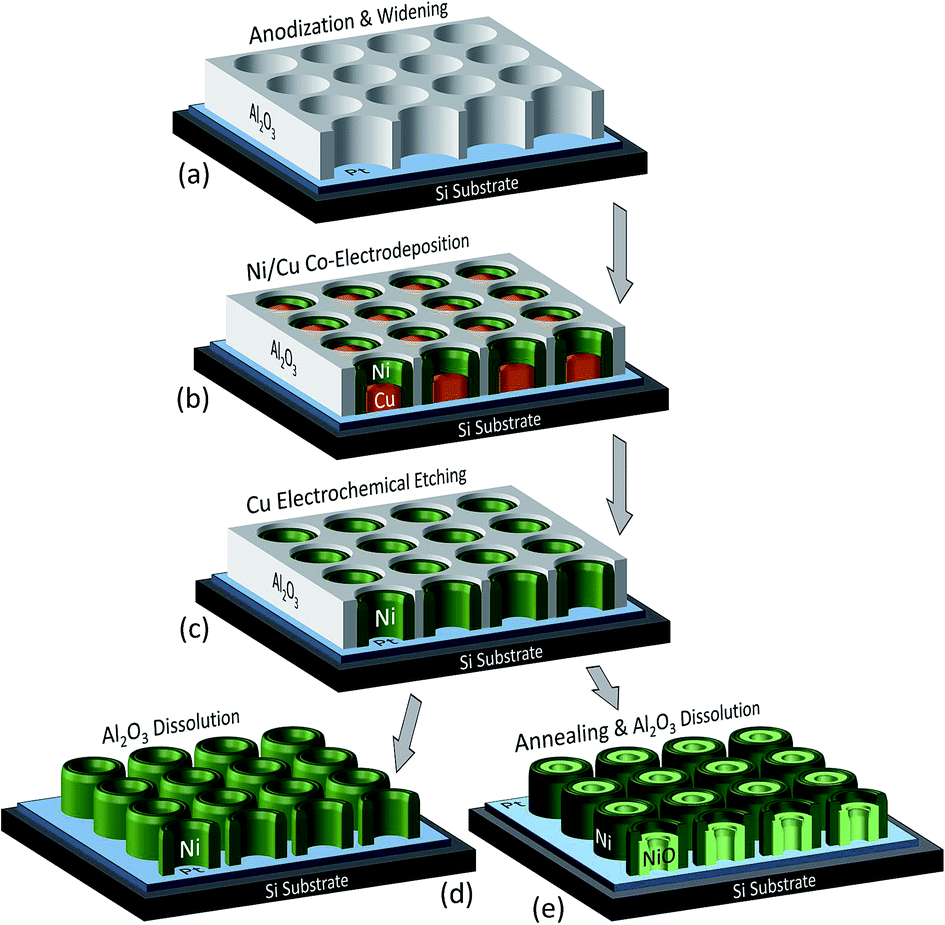 | ||
| Fig. 1 Schematic representation of the vertically-aligned heterostructured Ni/NiO NTs fabrication process. (a) Formation of the thin nanoporous AAO host supported on a Pt-coated Si substrate. (b) Cu/Ni core/shell NWs growth by co-ECD. (c) Cu core dissolution by electrochemical etching. (d) AAO film chemical dissolution, revealing Ni NTs perpendicularly-aligned to the Pt/Si substrate. (e) Thermal annealing step followed by AAO dissolution, generating heterostructured Ni/NiO NTs vertically-aligned to the Pt/Si substrate. | ||
The as-prepared substrate was next exposed to a single step anodization process in 0.3 M oxalic acid at 2 °C, by applying 60 V from a Keithley 2400 sourcemeter. The obtained nanopores were then chemically widened in 0.5 M H2SO4 at 40 °C for 2 h [Fig. 1(a)]. The resulting AAO film had a thickness of ∼1.4 μm, as well as a nanopores mean interspacing (D) of ∼150 nm and an average pores diameter (ϕ) of ∼110 nm, thus a porosity (P) of ∼50% estimated from:16
 | (1) |
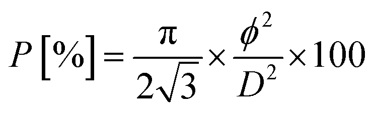
In a second stage, arrays of Cu/Ni core/shell NWs were grown in the pores of the supported AAO template [Fig. 1(b)] by co-electrodeposition (ECD).26,43 The core/shell NWs were co-synthesized at room temperature from an aqueous bath containing: 0.4 M Ni(H2NSO3)2·4H2O, 0.05 M CuSO4·5H2O and 0.1 M H3BO3. The process was carried out in a ‘three-electrodes’ potentiostatic configuration (using a PAR 263A Potentiostat) by applying to the working electrode (the substrate) −1 V versus a double-junction Ag/AgCl reference electrode (KCl saturated, E = 0.197 V), while a Pt foil was installed in the bath as a counter electrode. The process duration was adjusted to 65 s for an average length of the AAO-embedded core/shell NWs of ∼400 nm. The obtained cathodic reduction curve is depicted in Fig. 2(a), resembling the typical ECD behavior of an AAO-assisted chronoamperometric process, where the sharp current increase in the beginning is mainly related with the formation of a diffusion layer of cations in the solution and the NWs nucleation on the Pt cathode at the bottom of the pores, whilst the subsequent current plateau occurs when the gradient of ions concentration is equilibrated and is mainly associated with the NWs vertical growth within the AAO nanopores. The Cu/Ni core/shell NWs are obtained in specific conditions (applied potential and concentration ratio between the cations) due to a phase separation between the two metallic elements triggered by an existing miscibility gap in their solubility. Their vertical growth is thus supported by the different nucleation rates between the two phases, where the faster Cu reduction induces the initial formation of small Cu islands, while the Ni growth is progressively enhanced at the islands periphery as the solution is depleted from Cu cations.
 | ||
| Fig. 2 (a) Typical curve showing the cathodic reduction during the co-ECD of Cu/Ni core/shell NWs embedded within the supported AAO template. (b) Corresponding oxidation curve for the Cu core etching step. The insets show the two equivalent fabrication steps, as detailed in the text. | ||
Next, the Cu cores were electrochemically etched [Fig. 1(c)] using the same bath and configuration, by applying a positive potential of +0.2 V, while the Ni did not present a significant etching due to its passivation in sulfamate solutions,43–45 ultimately favoring the formation of Ni NTs. Fig. 2(b) shows the obtained oxidation current curve, where the sharp initial negative increase is attributed to the large amount of available Cu. Once the Cu anions concentration in the solution increases, the amount of solid Cu inside the Ni NTs reduces and the oxidation rate decreases determining the current to progressively approach zero once the Cu dissolution is finished.46
Noteworthy, the template synthesis confinement plays an important role in the formation of such coaxial Cu/Ni architectures with easily removable Cu cores. In particular, the co-ECD within nanopores as small as 50 nm determines the formation of complex mixed-phase NWs made up of a Cu–Ni alloy,44 as observed also in the case of thin films co-deposited electrochemically by template-free approaches where a subsequent Cu etching step triggers the occurrence of interesting Ni nodular structures with hollow cavities.35
Thermal treatments were ultimately performed using a Carbolite GTF 12/728 tube furnace in order to convert the subsequently obtained Ni NTs into heterostructured Ni/NiO NTs. The annealing steps were performed without removing the AAO host for preventing NTs outer radial expansion during the thermal oxidation stress, whilst the hollow tubular structure of the Ni nanoarchitectures allowed their inner thermal exposure. The samples were ramped with 5 °C min−1 at an annealing temperature of 450 °C, kept there for 30 min, 105 min and 240 min, respectively, and finally taken out from the oven and left to slowly cool down to room temperature.47
The AAO nanoporous host was optionally removed [Fig. 1(d) and (e)], before or after the thermal annealing procedures, mainly to allow subsequent morphological observations of the NTs. The AAO chemical etching was performed at room temperature in a 2 M NaOH solution for 15 min. The samples were afterwards carefully and thoroughly rinsed with DIW and then left to dry under atmospheric conditions for several hours.40
2.2 Samples characterization
Morphological observations of the samples were performed using a JEOL 7600F field-emission scanning electron microscope (SEM), equipped with transmission electron microscopy (STEM) capabilities. The STEM specimen was prepared by scratching the Ni NTs from the substrate and spreading them on a typical mesh support using tiny isopropanol droplets.Structural characterization of the NTs before and after the thermal conversion step was accomplished by using an X-ray diffraction (XRD) equipment operating with CuKα1 radiation (λ = 1.54056 Å).
Magnetic investigations were carried out by alternating gradient magnetometery (AGM), using a PMC MicroMag 2900 apparatus. Hysteresis loops and First-Order Reversal Curves (FORCs) were consequently obtained at room temperature with the magnetic field applied parallel and/or perpendicular to the NTs axis.
3 Results and discussion
3.1 Morpho-structural investigation
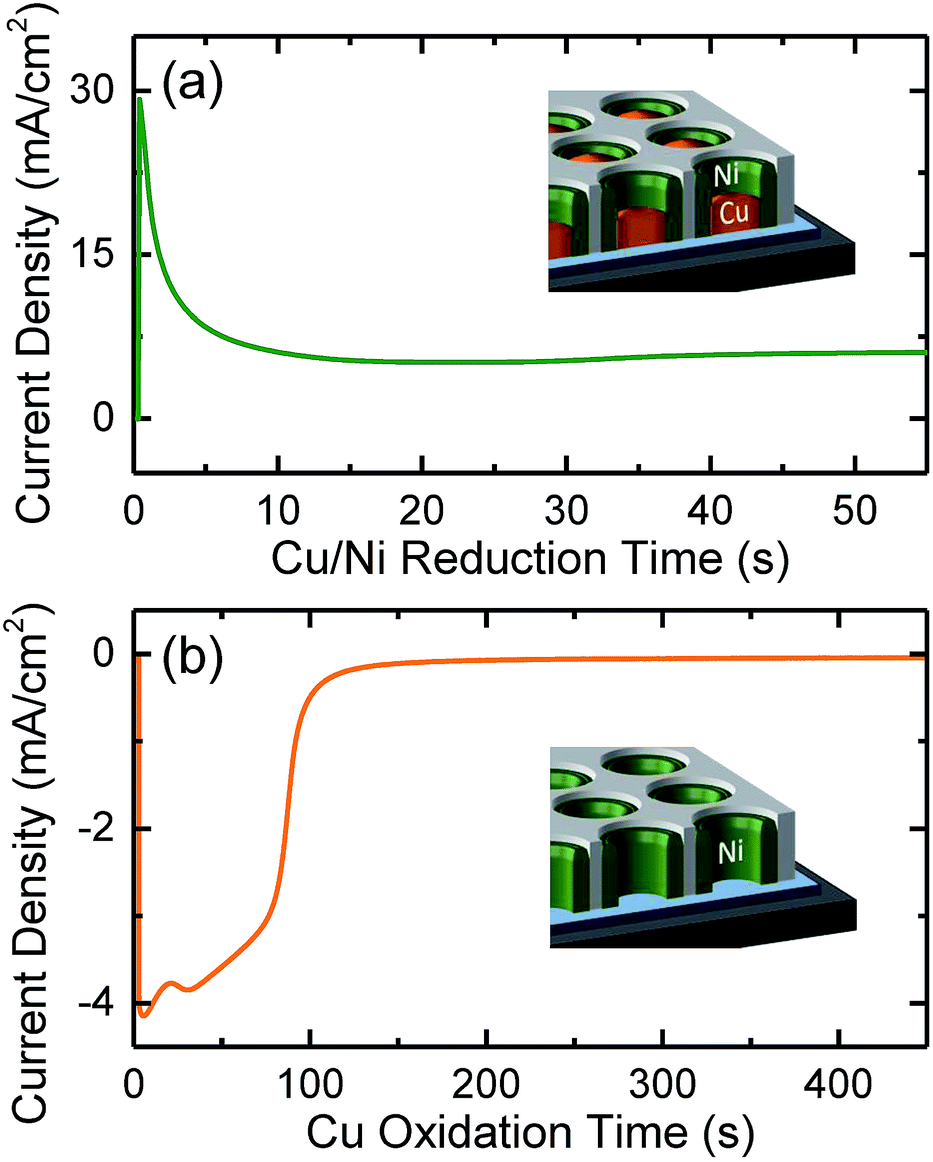
Fig. 3 shows the SEM top-view micrographs of the electrochemically-grown NTs, before (a and b) and after (c) a thermal annealing procedure at 450 °C for 105 min. The images were acquired after the complete dissolution of the AAO embedding template. As can be noticed, before the annealing step a dense array of Ni NTs perpendicularly-arranged to the substrate was obtained [Fig. 2(a) and (b)]. The as-prepared NTs exhibited an outer diameter of ∼110 nm (established by the mean diameter of the pores within the confining AAO template) and an inner diameter of ∼80 nm, thus leading to an average NTs wall thickness of ∼15 nm, as confirmed by the SEM observations. Next, additional STEM analysis pointed out that the obtained elongated Ni nanostructures exhibited indeed a homogenous tubular structure being hollow on their whole length [inset of Fig. 3(a)]. The NTs length was adjusted by mainly controlling the accumulated charge during the co-ECD process, at values around 400 nm. In addition, after the annealing step [Fig. 3(c)] the overall aspect morphology of the NTs was similar with the one observed before the annealing process. However, a slight reduction of the NTs inner diameter of several nm can be observed, whereas the outer diameter remained consistent with the result observed before the thermal treatment. The latter observation was attributed to the presence of the AAO host preventing the radial outer expansion of the NTs during the annealing procedure. Moreover, due to the very small initial wall thickness of the Ni NTs, the annealed Ni/NiO heterostructures remained opened, still resembling a tubular structure, although small irregularities seen in the inner diameter might suggest inhomogeneous oxidation of the initial Ni NTs wall. Under similar conditions, it was demonstrated elsewhere that the complete closure of the heterostructures wall might be reached for a total annealing duration of about 300 min.36 | ||
| Fig. 3 (a and b) SEM images at two different magnifications of the dense array of Ni NTs vertically-aligned on the substrate. The inset of (a) STEM image of a single Ni NT as-deposited on the specimen mesh. (c) Corresponding SEM image of the heterostructured Ni/NiO NTs obtained after an annealing treatment at 450 °C for 105 min. | ||
Fig. 4 shows the XRD spectra acquired from two substrates with vertically-aligned Ni NTs as-prepared (a) and heterostructured Ni/NiO NTs after annealing at 450 °C for 105 min (b), respectively. The typical Pt diffraction peaks at ∼39.5° and ∼46° corresponding to (111) and (200) Miller indices (JCPDS 04-0802), were observed in both situations being definitely attributed to the substrate. Despite the relatively broad and predominant Pt (111) peak, the common metallic Ni (111) phase at ∼44.5° was clearly observed on both non-annealed and annealed samples, although the additional Ni (200) peak at ∼52° was slightly enhanced only after the annealing process (JCPDS 01-1260), possibly due to Ni thermal re-crystallization mechanisms, as reported elsewhere.18,48 Furthermore, the annealing process complementarily generated a diffraction peak at ∼43.5° attributed to the NiO (200) crystal phase (JCPDS 22-1189) and thus demonstrating the partial conversion of the Ni NTs into heterostructured Ni/NiO NTs. The absence of the NiO (111) peak around 38° could be particularly explained by the presence of the broad Pt (111) peak within the XRD spectra. The obtained results can be also corroborated with the magnetic measurements presented in Section 3.2, that ultimately confirmed the formation of hybrid Ni/NiO NTs via the thermal annealing approach.
 | ||
| Fig. 4 XRD pattern of the NTs vertically-aligned to the substrate, before (a) and after (b) the annealing process performed at 450 °C for 105 min. | ||
3.2 Magnetic characterization
Fig. 5(a) shows the effect of annealing for the various samples on the hysteresis loops obtained at room temperature with the field applied parallel (∥) to the NTs axis. The data were normalized to the measured saturation magnetic moment for the non-annealed (reference) sample. In comparison with the reference sample, the annealed samples have shown a significant decrease of the saturation magnetic moment, to about 53%, 39% and 12% of the initial value for the samples annealed during 30 min, 105 min and 240 min, respectively. Such evolution was due to the progressive oxidation of the Ni NTs during the annealing process. Fig. 5(b) and (c) compare the room temperature hysteresis loops along ∥ and perpendicular (⊥) direction to the NTs axis, for the reference sample and for the sample annealed during 105 min. It was found that the non-annealed sample exhibited an easy plane of magnetization, with a normalized remanent magnetization (squareness) Mr/Ms of 0.19 and 0.33, as well as coercive fields (Hc) of 160 Oe and 180 Oe, for the field applied ∥ and ⊥ to the NTs axis, respectively [see Fig. 5(b)]. Subsequently, the annealing process led to a change in easy axis from ⊥ to ∥ to the NTs axis, as illustrated for the sample annealed during 105 min. Along the NTs axis, Mr/Ms increased from 0.19 up to 0.53 and the coercive field also raised from 160 Oe up to 310 Oe [see Fig. 5(c)]. The same qualitative behavior was found for the sample annealed during 30 min (Mr/Ms = 0.4 and Hc = 310 Oe). In contrast, the annealing caused no appreciable change in the shape of the hysteresis loops along the ⊥ direction. Therefore, the annealing process led to an increase in the effective shape anisotropy as evidenced by the less sheared hysteresis loops along the ∥ direction to the NTs axis [see Fig. 5(a)], thus reinforcing the latter as the easy axis. For an assembly of high aspect ratio nanoparticles, it is known that the effective anisotropy results from the anisotropy of the particle lowered by the DIF between them, i.e. antiferromagnetic interaction in the case of parallel arrays of NTs.26,49 Since the shape anisotropy in such elongated nanomagnets is not modified by the annealing process, the enhancement of the shape anisotropy can be then attributed to a decrease of the DIF, which is known to directly depend on the effective filling factor of particles in the array.49 Furthermore, since the distance between NTs and outer diameter remained constant during the annealing process, the reduction of the DIF along the NTs axis and consequently the enhancement of the shape anisotropy ruled out the hypothesis of the uniform oxidation of the Ni NTs. On the contrary, our results are consistent with an oxidation of the inner surface of the NTs which results in a reduction of the wall thickness of the non-oxidized Ni NTs in contact with the pore walls of the AAO template. Indeed, it was demonstrated both theoretically and experimentally that the cavities in NT assemblies reduces the DIF when compared with NW assemblies and the derived expressions also predicted that the DIF is further reduced as the wall thickness of the ferromagnetic NTs becomes smaller.25,26 Such a scenario involving the growth of heterostructured Ni/NiO NTs through annealing was consistent with the observed magnetic behavior in the present study.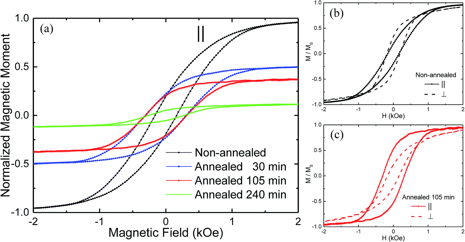 | ||
| Fig. 5 (a) Typical hysteresis loops measured along parallel (∥) direction to the NTs axis, showing the decrease of the saturation magnetic moment with the annealing time. The data were normalized to the measured saturation magnetic moment for the non-annealed (reference) sample. (b and c) Corresponding hysteresis loops acquired parallel (∥) and perpendicular (⊥) to the NTs axis for the reference sample (b) and for the sample annealed at 450 °C for a duration of 105 min (c). | ||
In order to provide quantitative estimation of the DIF changes during all stages of the annealing process, the AGM was employed to measure a large number (about 150) of FORCs along the NTs axis. In this context, after saturation the magnetization (M) was measured starting from a reversal field (Hr) back to the positive saturation, tracing out a FORC referred as M(H,Hr). A family of FORCs was then measured at different Hr, with an equal field spacing, thus filling the interior of the major hysteresis loop, as shown in Fig. 6(a)–(c) for the three different NTs array samples. The FORC diagrams were calculated by a mixed second order derivative, as proposed by R. Pike:50
 | (2) |
| αZ = NxMsPNT | (3) |
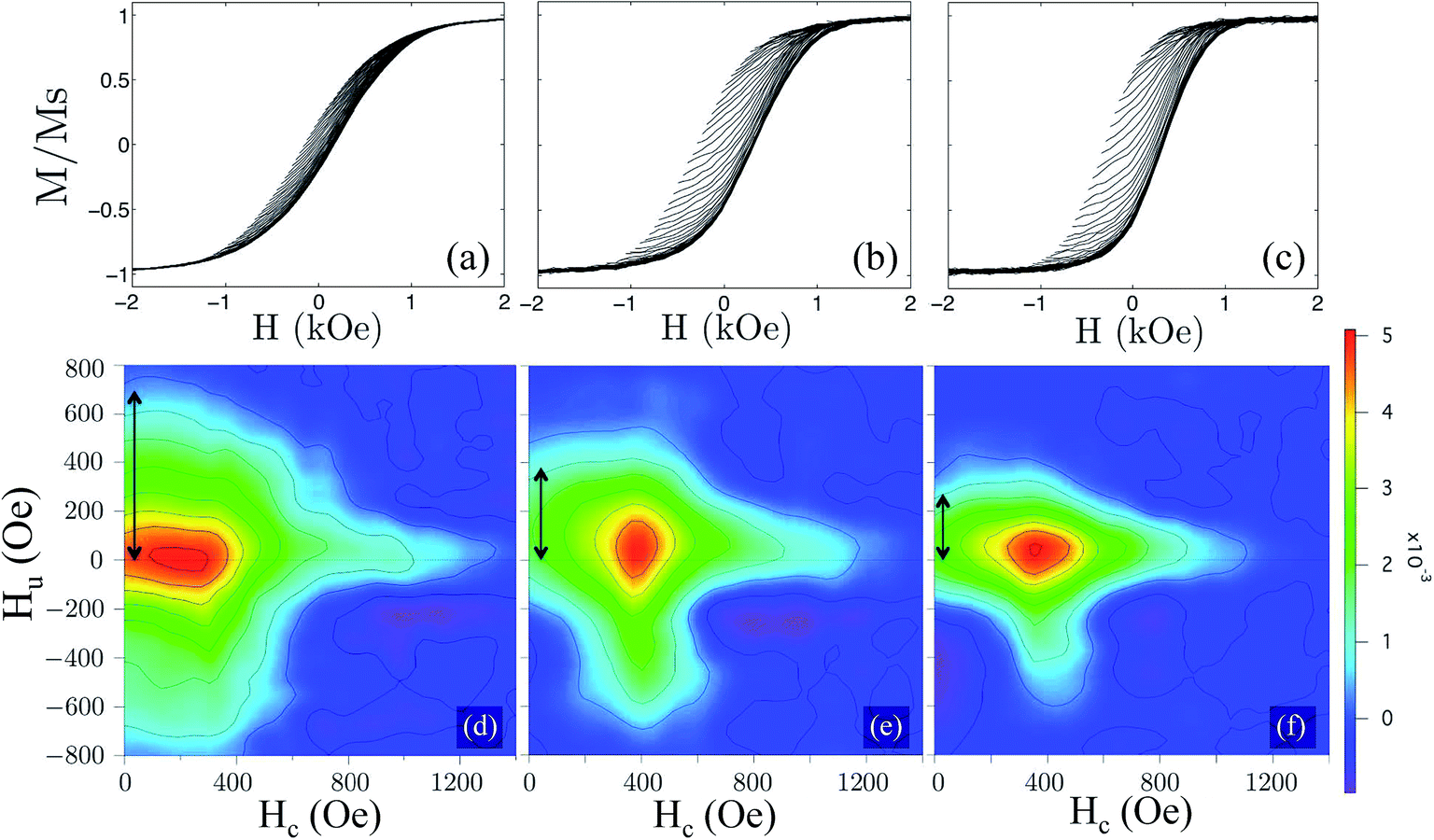 | ||
| Fig. 6 (a–c) Magnetization curves and (d–f) corresponding First-Order Reversal Curves (FORCs) obtained for the Ni NT arrays when applying the magnetic field ∥ to the NTs axis, for the reference sample (a and d), as well as after annealing durations of 30 min (b and e) and 105 min (c and f) at T = 450 °C. The vertical arrows in the FORC diagrams indicate the magnitude of the dipolar interaction field (DIF), as detailed in the text. | ||
4 Conclusions
In this work we developed an efficient and cost-effective pathway in which large and dense ferromagnetic arrays of vertically-aligned heterostructured Ni/NiO NTs can be produced. The method allowed the fabrication of hybrid hollow elongated nanostructures without compromising their verticality to the substrate, as well as their initial tubular integrity. Using adequately adapted AGM measurements, we demonstrated the ability to tune the DIF value within the magnetic array, just by slightly changing the thickness of the antiferromagnetic NiO thermally-grown layer. Furthermore, the subsequent FORCs-based analysis permitted an estimation of the DIF coefficients which were in close agreement with the calculated values among the thermally annealed samples, proving further the hypothesis of retaining a tubular hybrid structure of the Ni/NiO NTs after the thermal conversion process of the AAO-embedded Ni NTs. Such dense arrays of ferromagnetic NTs may therefore potentially withstand individual magnetic addressability, by carefully tuning the DIF value in terms of changing the magnetic packing fraction either by adjusting the template porosity, or ultimately by controlling the degree of NTs thermal conversion step. The entire fabrication protocol is quite promising and amiable to further optimisations, opening an outstanding way towards direct integrability of devices relying on large magnetic arrays of vertically-standing elongated nanostructures.Acknowledgements
This work was partly supported by the ‘Fédération Wallonie-Bruxelles’ (ARC 13/18-052, Supracryst) and by the ‘Fonds de la Recherche Scientifique’ – FNRS under Grant No. T.0006.16. The authors thank Mrs Anne Iserentant (Earth and Life Institute, Université Catholique de Louvain) and Prof. Lucian Ion (Faculty of Physics, University of Bucharest) for the XRD measurements and data interpretation.References
- L. Vila, P. Vincent, L. D.-D. Pra, G. Pirio, E. Minoux, L. Gangloff, S. Demoustier-Champagne, N. Sarazin, E. Ferain, R. Legras, L. Piraux and P. Legagneux, Nano Lett., 2004, 4, 521–524 CrossRef CAS.
- H. Qi, O. J. Glembocki and S. M. Prokes, J. Nanomater., 2012, 2012, 7 Search PubMed.
- A. Koka, Z. Zhou and H. A. Sodano, Energy Environ. Sci., 2014, 7, 288–296 CAS.
- A. Koka and H. A. Sodano, Nat. Commun., 2013, 4, 2682 Search PubMed.
- E. A. Anyebe, A. M. Sanchez, S. Hindmarsh, X. Chen, J. Shao, M. K. Rajpalke, T. D. Veal, B. J. Robinson, O. Kolosov, F. Anderson, R. Sundaram, Z. M. Wang, V. Falko and Q. Zhuang, Nano Lett., 2015, 15, 4348–4355 CrossRef CAS PubMed.
- K. M. Razeeb, M. Jamal, M. Hasan and A. Mathewson, Nanobiosensors and Nanobioanalyses, Springer, Japan, Tokyo, 2015, pp. 23–40 Search PubMed.
- T. Berthing, C. B. Sørensen, J. Nygård and K. L. Martinez, J. Nanoneurosci., 2009, 1, 3–9 CrossRef CAS.
- B. Sanz, E. M. Palmero, R. P. del Real, M. Vázquez and C. Mijangos, Ind. Eng. Chem. Res., 2015, 54, 13005–13008 CrossRef CAS.
- W. B. Choi, D. S. Chung, J. H. Kang, H. Y. Kim, Y. W. Jin, I. T. Han, Y. H. Lee, J. E. Jung, N. S. Lee, G. S. Park and J. M. Kim, Appl. Phys. Lett., 1999, 75, 3129–3131 CrossRef CAS.
- H. Chen, A. Roy, J. B. Baek, L. Zhu, J. Qu and L. Dai, Mater. Sci. Eng., R, 2010, 70, 63–91 CrossRef.
- A. Z. Liao, C. W. Wang, J. B. Chen, X. Q. Zhang, Y. Li and J. Wang, Mater. Res. Bull., 2015, 70, 988–994 CrossRef CAS.
- T. Stergiopoulos, A. Ghicov, V. Likodimos, D. S. Tsoukleris, J. Kunze, P. Schmuki and P. Falaras, Nanotechnology, 2008, 19, 5602 CrossRef PubMed.
- H. Cao, L. Wang, Y. Qiu, Q. Wu, G. Wang, L. Zhang and X. Liu, ChemPhysChem, 2006, 7, 1500–1504 CrossRef CAS PubMed.
- Y. Zhong, H. Fan, L. Chang, H. Shao, J. Wang, J. Zhang and C. Cao, J. Power Sources, 2015, 296, 255–260 CrossRef CAS.
- S. J. Son, J. Reichel, B. He, M. Schuchman and S. B. Lee, J. Am. Chem. Soc., 2005, 127, 7316–7317 CrossRef CAS PubMed.
- K. Nielsch, F. J. Castaño, S. Matthias, W. Lee and C. A. Ross, Adv. Eng. Mater., 2005, 7, 217–221 CrossRef CAS.
- K. Pitzschel, J. Bachmann, J. M. Montero-Moreno, J. Escrig, D. Görlitz and K. Nielsch, Nanotechnology, 2012, 23, 495718 CrossRef PubMed.
- A. Vlad, M. Mátéfi-Tempfli, V. A. Antohe, S. Faniel, N. Reckinger, B. Olbrechts, A. Crahay, V. Bayot, L. Piraux, S. Melinte and S. Mátéfi-Tempfli, Small, 2008, 4, 557–560 CrossRef CAS PubMed.
- A. Vlad, V. A. Antohe, J. M. Martinez-Huerta, E. Ferain, J. F. Gohy and L. Piraux, J. Mater. Chem. A, 2016, 4, 1603–1607 CAS.
- M. Sharma, B. K. Kuanr, V. Veerakumar, A. Basu and Z. J. Celinski, IEEE Trans. Magn., 2014, 50, 1–4 Search PubMed.
- R. Sharif, S. Shamaila, M. Ma, L. D. Yao, R. C. Yu, X. F. Han and M. K. ur Rahman, Appl. Phys. Lett., 2008, 92, 2505 CrossRef.
- P. Landeros, S. Allende, J. Escrig, E. Salcedo, D. Altbir and E. E. Vogel, Appl. Phys. Lett., 2007, 90, 2501 CrossRef.
- X. F. Han, S. Shamaila, R. Sharif, J. Y. Chen, H. R. Liu and D. P. Liu, Adv. Mater., 2009, 21, 4619–4624 CrossRef CAS.
- A. Pereira, J. L. Palma, J. C. Denardin and J. Escrig, Nanotechnology, 2016, 27, 345709 CrossRef PubMed.
- M. P. Proenca, C. T. Sousa, J. Escrig, J. Ventura, M. Vazquez and J. P. Araujo, J. Appl. Phys., 2013, 113, 3907 CrossRef.
- Y. Velázquez-Galván, J. M. Martínez-Huerta, J. D. L. T. Medina, Y. Danlée, L. Piraux and A. Encinas, J. Phys.: Condens. Matter, 2014, 26, 6001 CrossRef PubMed.
- V. Skumryev, S. Stoyanov, Y. Zhang, G. Hadjipanayis, D. Givord and J. Nogués, Nature, 2003, 423, 850–853 CrossRef CAS PubMed.
- K. Yadav, B. R. Mehta and J. P. Singh, J. Mater. Chem. C, 2014, 2, 6362–6369 RSC.
- R. S. Chen, H. M. Chang, Y. S. Huang, D. S. Tsai, S. Chattopadhyay and K. H. Chen, J. Cryst. Growth, 2004, 271, 105–112 CrossRef CAS.
- G. Malandrino, L. M. S. Perdicaro, I. L. Fragalà, R. L. Nigro, M. Losurdo and G. Bruno, J. Phys. Chem. C, 2007, 111, 3211–3215 CAS.
- S. H. Yu, J. Shin, J. J. Kim, K. J. Lee and Y. E. Sung, RSC Adv., 2012, 2, 12177–12181 RSC.
- H. M. Ouyang, G. T. Fei, Y. Zhang, H. Su, Z. Jin, S. H. Xu and L. D. Zhang, J. Mater. Chem. C, 2013, 1, 7498–7506 RSC.
- J. Choi, J. H. Lim, J. Lee and K. J. Kim, Nanotechnology, 2007, 18, 055603 CrossRef.
- K. Xie, M. Guo, H. Huang and Y. Liu, Corros. Sci., 2014, 88, 66–75 CrossRef CAS.
- X. Dai, D. Chen, H. Fan, Y. Zhong, L. Chang, H. Shao, J. Wang, J. Zhang and C. n. Cao, Electrochim. Acta, 2015, 154, 128–135 CrossRef CAS.
- F. I. Dar, K. Moonoosawmy and M. Es-Souni, Nanoscale Res. Lett., 2013, 8, 363 CrossRef PubMed.
- J. Bao, C. Tie, Z. Xu, Q. Zhou, D. Shen and Q. Ma, Adv. Mater., 2001, 13, 1631–1633 CrossRef CAS.
- F. Tao, M. Guan, Y. Jiang, J. Zhu, Z. Xu and Z. Xue, Adv. Mater., 2006, 18, 2161–2164 CrossRef CAS.
- C. Mu, Y. X. Yu, R. M. Wang, K. Wu, D. S. Xu and G. L. Guo, Adv. Mater., 2004, 16, 1550–1553 CrossRef CAS.
- V. A. Antohe, A. Radu, M. Mátéfi-Tempfli, A. Attout, S. Yunus, P. Bertrand, C. A. Duţu, A. Vlad, S. Melinte, S. Mátéfi-Tempfli and L. Piraux, Appl. Phys. Lett., 2009, 94, 3118 CrossRef.
- F. A. Araujo, L. Piraux, V. A. Antohe, V. Cros and L. Gence, Appl. Phys. Lett., 2013, 102, 2402 Search PubMed.
- L. Piraux, K. Renard, R. Guillemet, S. Mátéfi-Tempfli, M. Mátéfi-Tempfli, V. A. Antohe, S. Fusil, K. Bouzehouane and V. Cros, Nano Lett., 2007, 7, 2563–2567 CrossRef CAS PubMed.
- Q. Wang, G. Wang, X. Han, X. Wang and J. G. Hou, J. Phys. Chem. B, 2005, 109, 23326–23329 CrossRef CAS PubMed.
- Z. Liu, G. Xia, F. Zhu, S. Kim, N. Markovic, C. L. Chien and P. C. Searson, J. Appl. Phys., 2008, 103, 4313 Search PubMed.
- Z. Liu, D. Elbert, C. L. Chien and P. C. Searson, Nano Lett., 2008, 8, 2166–2170 CrossRef CAS PubMed.
- J. K. Chang, S. H. Hsu, I. W. Sun and W. T. Tsai, J. Phys. Chem. C, 2008, 112, 1371–1376 CAS.
- S. Han, H. Y. Chen, C. C. Chen, T. N. Yuan and H. C. Shih, Mater. Lett., 2007, 61, 1105–1108 CrossRef CAS.
- L. D. L. S. Valladares, A. Ionescu, S. Holmes, C. H. W. Barnes, A. B. Domínguez, O. A. Quispe, J. C. González, S. Milana, M. Barbone, A. C. Ferrari, H. Ramos and Y. Majima, J. Vac. Sci. Technol., B: Nanotechnol. Microelectron.: Mater., Process., Meas., Phenom., 2014, 32, 051808 Search PubMed.
- A. Encinas-Oropesa, M. Demand, L. Piraux, I. Huynen and U. Ebels, Phys. Rev. B: Condens. Matter Mater. Phys., 2001, 63, 4415 CrossRef.
- C. R. Pike, A. P. Roberts and K. L. Verosub, J. Appl. Phys., 1999, 85, 6660–6667 CrossRef CAS.
- G. Bertotti, in Hysteresis in Magnetism, Academic Press, San Diego, 1998, pp. 129–162 Search PubMed.
- F. Béron, L. Clime, M. Ciureanu, D. Ménard, R. W. Cochrane and A. Yelon, J. Nanosci. Nanotechnol., 2008, 8, 2944–2954 CrossRef.
- C. I. Dobrotă and A. Stancu, J. Appl. Phys., 2013, 113, 3928 CrossRef.
- D. A. Gilbert, G. T. Zimanyi, R. K. Dumas, M. Winklhofer, A. Gomez, N. Eibagi, J. L. Vicent and K. Liu, Sci. Rep., 2014, 4, 4204 Search PubMed.
- J. M. Martínez-Huerta, J. D. L. T. Medina, L. Piraux and A. Encinas, J. Phys.: Condens. Matter, 2013, 25, 6003 CrossRef PubMed.
- R. Cai, V.-A. Antohe, Z. Hu, B. Nysten, L. Piraux and A. M. Jonas, Adv. Mater., 2017, 29, 1604604 CrossRef PubMed.
Footnotes |
| † Currently at: Institut für Physik, Universität Augsburg, Germany. |
| ‡ Currently at: Instituto de Física, Universidad Autónoma de San Luis Potosí, Mexico. |
| This journal is © The Royal Society of Chemistry 2017 |