DOI:
10.1039/C7RA01236E
(Paper)
RSC Adv., 2017,
7, 14219-14223
Field emission properties of Al-doped ZnO nanosheet based on field emitter device with UV exposure
Received
28th January 2017
, Accepted 24th February 2017
First published on 2nd March 2017
Abstract
In this study, aluminum (Al)-doped zinc oxide (ZnO) nanosheets were synthesized on a ZnO/glass substrate under different growth temperatures using a modified aqueous solution method. The field emission and physical properties of Al-doped ZnO nanosheets were then investigated. Results indicated that high growth temperature improves the quality of Al-doped ZnO nanosheets. Moreover, the photoluminescence intensity of the sample's ultraviolet (UV) emission peak (growth temperature at 60 °C) was stronger compared with those of other samples. However, its broad, deep-level green emission band was weaker. The turn-on field and field enhancement factor (β) of Al-doped ZnO nanosheets were 3.8 V μm−1 and 4760, respectively. The UV illumination of the Al-doped ZnO nanosheets decreased the turn-on electrical field from 3.8 to 3.3 V μm−1 and elevated the β from 4760 to 7501.
I. Introducion
Field emission-based displays and electronic device applications have been studied for decades and have continued to attract interest because of their potential applications in flat panel displays, vacuum microwave amplifiers, and lamps. These applications are commonly used in everyday living, medicine, and research.1–3 The advantages and disadvantages of field emission devices can be attributed to their geometrical structures and material properties. These characteristics include one-dimensional nanostructures, which offer low work function, high mechanical stability, conductivity, and aspect ratios.4,5 Recently, one-dimensional nanostructures (nanowires, nanorods, and nanotips) have been developed as electron field emitters because of their negative electron affinity, high mechanical strength, and chemical stability. Zinc oxide (ZnO) nanostructures have been extensively studied because of their remarkable physical and chemical properties that can be exploited in various electronic and optoelectronic devices. ZnO nanostructures with different geometrical morphologies have been enhanced using diverse synthetic methods, such as chemical vapor deposition, hydrothermal method, pulsed laser deposition, and furnace and electrochemical deposition.6–10 The performance of field emission-based devices has been improved by doping with various metal elements, such as aluminum (Al), gallium, and indium. Field emission-based devices with improved performance have potential applications in optoelectronic devices and enhanced optical and electrical properties.11–14 It has been reported that field emission properties are mainly dependent on the dimension, morphology, and apex geometry of one-dimensional nanostructure. Recently, one-dimensional ZnO nanostructures have been discussed for the field emission device, such as Z. Zhang et al. reported the influence of morphologies and doping of nanostructured ZnO on the field emission behaviors by using metal–organic chemical vapor deposition (>600 °C).15 F. Ye et al. reported field emission of Al-doped ZnO films by using DC magnetron sputtering.16 K. Mahmood et al. reported the enhanced and stable field emission behavior of a novel electrosprayed Al-doped ZnO bilayer film by using electrosprayed method (>160 °C).17 C. L. Hsu et al. reported enhanced field emission of Al-doped ZnO nanowires grown on a flexible polyimide substrate by using hydrothermal method (>90 °C).18 However, it is very rare that study and low temperature fabrication of two dimensional Al-doped ZnO nanostructure. In the study, well-aligned 2D Al-doped ZnO nanosheets were synthesized on a glass substrates by low-temperature (<70 °C) aqueous solution method.
II. Experimental
Prior to preparation, the glass substrate was cleaned with a standard cleaning process. Then, the substrates were dried in an oven. Using the two-step deposition process, a 25 nm-thick ZnO seed layer was first deposited onto a glass substrate through RF magnetron sputtering system. The size of the target was a 3-inch ZnO (99.99%). The base pressure was 5 × 10⁻⁶ torr. Argon and oxygen flow rates were maintained at 18 and 2 sccm, respectively. The chamber's working pressure was maintained at 1 × 10⁻² torr. Radio frequency power was maintained at 100 W during the 5 min deposition process. In the second step of deposition, Al-doped ZnO nanosheets with four different parameters were grown using a modified aqueous solution method. This step was performed in a beaker with 0.1 M zinc (Zn) nitrate hexahydrate and 0.4 M sodium hydroxide. The Al dopant was added as Al nitrate at 1% equimolar concentration. The growth solution was constantly stirred for 1 h at 40 °C, 50 °C, and 60 °C. Finally, the sample was washed with deionized water and dried at room temperature. Before the examination of the field emission characteristics, a 100 nm-thick Ag film was deposited onto the Al-doped ZnO nanosheets using an electron-beam evaporator. The Ag film acted as the contact electrode.
The surface morphologies of the Al-doped ZnO nanosheets were observed with a field emission scanning electron microscope (FESEM, Hitachi-S-4800-I). The crystallinity of Al-doped ZnO nanosheets was analyzed with an X-ray diffractometer (XRD, Bruker D8 advance). The field emission properties of the Al-doped ZnO nanosheets were examined using a Keithley 2410 System in a homemade vacuum chamber. Pressure was maintained at less than 5 × 10⁻⁶ torr in the chamber. A 5 mm (L) × 30 mm (W) indium (In) tin oxide glass functioned as the anode and the Al-doped ZnO nanosheet served as the cathode. The anode–cathode distance was 140 μm. To measure emission current, a 0–1100 V was applied into the devices in 10 V increments by Keithley 2410 System.
III. Results and discussion
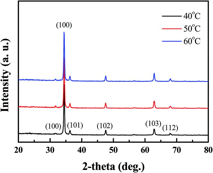
Fig. 1 shows the typical XRD pattern of Al-doped ZnO nanosheets prepared under different temperatures on a ZnO/glass substrate. The sharp diffraction peaks from the Al-doped ZnO nanosheets were attributed to hexagonal wurtzite ZnO (JCPDS card no. 36-1451). The (002) diffraction peak intensity was considerably stronger compared with those of the other peaks. This finding indicated that the Al-doped ZnO nanosheet crystals preferentially grew along the c-axis, which was perpendicular to the substrate surface. Moreover, all samples, which were prepared under different temperatures, displayed a (002) peak with full-width at half-maximum (FWHM) values of 0.2913 (sample 1), 0.27336 (sample 2), and 0.27142 (sample 3). This result suggested that the quality of Al-doped ZnO nanosheets can be improved by high growth temperatures. In addition, no other diffraction peaks were observed in the samples, which suggested the absence of impurities and the complete transformation of the precursor into the ZnO phase.
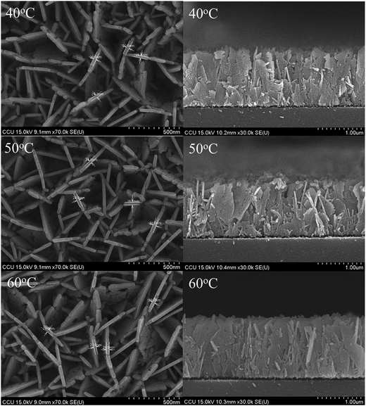 |
| | Fig. 1 FESEM images of AZO nanosheets samples, which the growth temperature from 40 °C to 60 °C. | |
Fig. 2 exhibits the FE-SEM images of Al-doped ZnO nanosheets prepared on a ZnO/glass substrate under varying growth temperatures. The images show that high-density nanosheets were successfully grown on the ZnO/glass substrate. The nanosheets were connected to each other as net-shaped films. Most nanosheets were oriented perpendicular to the substrate surface. This alignment is strongly consistent with the strong (002) diffraction peak intensity observed in the XRD pattern. The thickness and length of the Al-doped ZnO nanosheets were approximately 23–32 nm and 1.34 μm, 24–31 nm and 1.33 μm, and 23–29 nm and 1.44 μm for samples 1, 2, and 3, respectively. These findings demonstrated that morphology of the sheets did not significantly change in response to growth temperature.
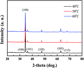 |
| | Fig. 2 XRD patterns of AZO nanosheets samples, which the growth temperature from 40 °C to 60 °C. | |
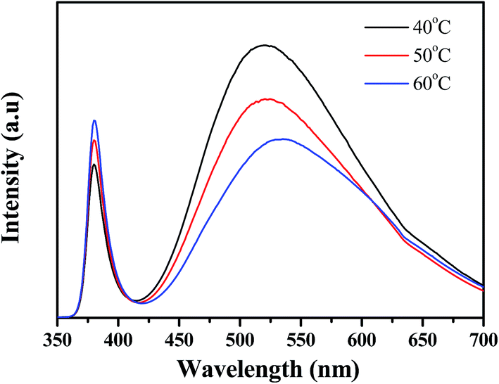
Fig. 3 presents the room-temperature photoluminescence (PL) spectrum of Al-doped ZnO nanosheet samples after excitation with a He–Cd laser. The typical luminescence behavior of ZnO nanostructures produced a narrow ultraviolet (UV) emission peak and a broad green emission band. The figure clearly shows a peak at approximately 380 nm and a broad deep-level emission at 500–600 nm. The sample's UV emission peaks are attributed to the combination of free excitons caused by exciton–exciton collision (∼3.3 eV).19 Deep-level defects, such as oxygen vacancies, oxygen interstitials, Zn vacancies, and Zn interstitials, were found at approximately 2.06 to 2.5 eV.20–22 The sample displayed stronger UV emission peak intensity (growth temperature at 60 °C) than those of other samples. However, its broad, deep-level green emission band was also weaker. The nanostructure's structural quality can be evaluated with the ratio of UV emission intensity to deep-level emission intensity, which is denoted as Q in this paper. The calculated Q values of the samples were 0.5627 (sample 1), 0.812 (sample 2), and 1.103 (sample 3) for Al-doped ZnO nanosheets at different growth temperatures. This difference likely resulted from interactions between Al and Zn ions and increased growth temperatures. These two conditions, which consumed oxygen ions, decreased the concentration of interstitial oxygen in the Al-doped ZnO nanosheets.
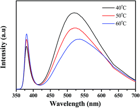 |
| | Fig. 3 Presents the room-temperature photoluminescence (PL) spectrum of Al-doped ZnO nanosheet samples after excitation with a He–Cd laser, which the growth temperature from 40 °C to 60 °C. | |
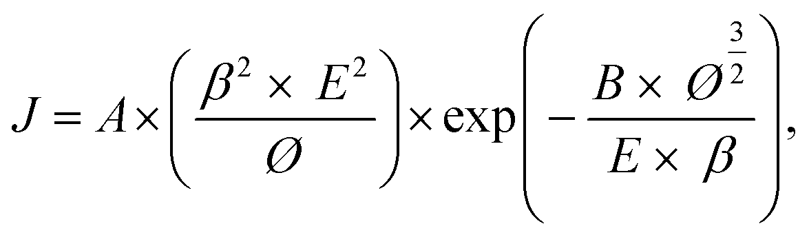
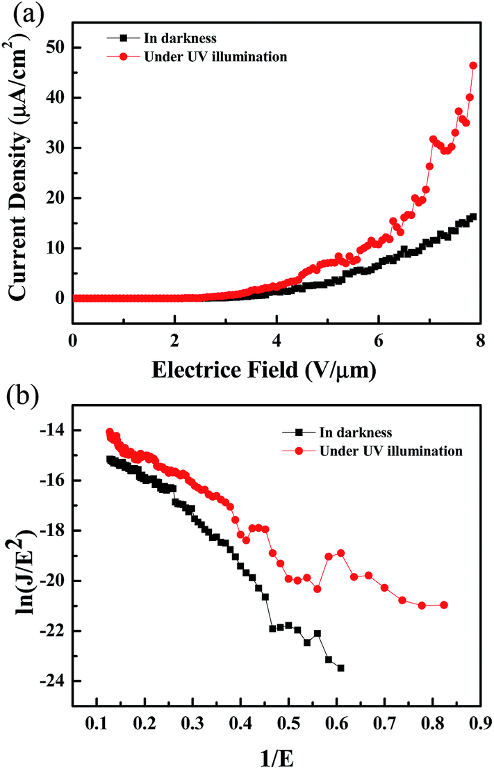
Table 1 presents the results of the physical property analysis. The results revealed that sample 3 had the best physical properties among all samples. Therefore, sample 3 was used in the subsequent experiments. A field emission device was examined in a vacuum chamber that was evacuated to a base pressure of <5 × 10⁻⁶ mtorr. The as-prepared nanostructures on the glass substrate (25 mm2) were utilized as a cathode and the indium-doped tin oxide glass plate served as the anode. The current density curves of the Al-doped ZnO nanosheet device in the dark and under UV illumination (wavelength = 365 nm) are presented in Fig. 4(a). In this figure, the density curves are plotted the as a function of applied field (J–E). To further determine the field emission measurements of the Al-doped ZnO nanosheets, the measured current density electric field curves were analyzed using the Fowler–Nordheim (F–N) equation:23
| |
 | (1) |
where
J is the current density;
E is the applied field between the anode and cathode;
A and
B are the constants (
A = 1.56 × 10
−10 A V
−2 eV,
B = 6.83 × 10
9 V eV
−3/2 μm
−1);
Ø is the work function of the emitting material, which is approximately 5.3 eV for ZnO;
24 and
β is the effective field enhancement factor. The turn-on field was defined as the electric field that corresponds to a 10
−6 A cm
−2 current density. The turn-on electric fields of the device were 3.8 V μm
−2 in the dark and 3.3 V μm
−2 under UV illumination (see
Table 2). We further simplified the F–N equation to thoroughly investigate the effect of field enhancement factor:
25| |
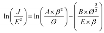 | (2) |
Table 1 Presents the results of the physical property analysis
| Growth temperature |
Length (μm) |
Thickness (nm) |
XRD (002) peak to FWHM value |
Q value |
| 40 °C (sample 1) |
1.34 |
24–32 |
0.2913 |
0.5627 |
| 50 °C (sample 2) |
1.33 |
24–31 |
0.27336 |
0.812 |
| 60 °C (sample 3) |
1.44 |
23–29 |
0.27142 |
1.103 |
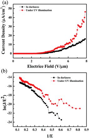 |
| | Fig. 4 (a) Field emission characteristics and (b) F–N plot of ln(J/E2) versus 1/E of as-synthesized AZO nanosheets for the sample 3. | |
Table 2 Presents the results of the field emission property analysis for the sample 3
| Sample 3 |
Turn-on (E = V μm−1) |
Slope |
β |
| In darkness |
3.8 |
17.507 |
4760 |
| Under UV illumination |
3.3 |
11.109 |
7501 |
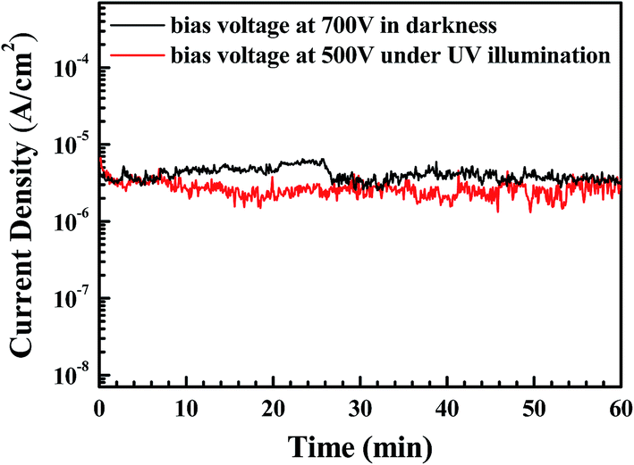
The field enhancement factor, or the work function, could be calculated with this equation. If the work function was 5.3 eV for ZnO, the field enhancement factors of the Al-doped ZnO nanosheets are approximately 4760 in the dark and 7501 under UV illumination, as shown in Fig. 4(b). According to the literature doping with aluminum greatly improved the field emission properties which mainly due to increase carrier concentration while aluminum doped in ZnO nanosheets by liberating more electrons. When an electric field was applied to the sample, the conductor band was bent to the Fermi level and the electrons tunneled to the vacuum level. Then, the carrier concentration increase with Al doped into the ZnO nanosheet, the more carriers exist in the conduction band. Moreover, as the Al-doped ZnO nanosheets was illuminated by UV light, a larger number of electron–hole pairs were generated and numerous electrons transferred to the conduction band, and the electric field was established between the Al-doped ZnO nanosheet and the vacuum became larger, greater numbers of electrons moved toward the Al-doped ZnO nanosheet edges. These obtained values were considerably higher compared with the values recently reported by other groups, as reported in Table 3.26–31 These results demonstrated the excellent long-term emission current stability of the Al-doped ZnO nanostructures. Fig. 5 illustrates the field emission device stability of the device in the dark and under UV. The current density was monitored for 3600 s with an initial emission current density of 10−6 A cm−2. The emission currents under UV varied because the electrons that were excited via UV illumination were not very stable. Thus, electrons were rapidly generated and recombined under UV illumination.
Table 3 Field-emission characteristics of different nanostructure field emitters recently reported in the open literature
| Nanostructure |
Turn-on (V μm−1) |
Field enhancement β (×103) |
Reference no. |
| ZnO nanorods |
9.2 |
0.87 |
26 |
| Tapered ZnO nanorods |
7.9 |
1 |
26 |
| ZnO nanowires |
5.1 |
1.7 |
27 |
| GaN nanowires |
8.4 |
0.47 |
28 |
| ZnO nanoneedles |
4.1 |
1.134 |
29 |
| ZnO nanocones |
6.2 |
2.252 |
30 |
| Tapered ZnS nanostructures |
11.2 |
2.54 |
31 |
| AZO nanosheets |
3.8 |
4.76 |
In this work |
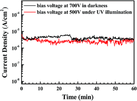 |
| | Fig. 5 Test of stability of emission current in the dark and under UV illumination. | |
IV. Conclusions
Using various growth temperatures, Al-doped ZnO nanosheets were synthesized on ZnO/glass substrate in aqueous solution. The field emission and physical properties of Al-doped ZnO nanosheets were then analyzed. The results of the analysis demonstrated that high temperatures improved the quality of the Al-doped ZnO nanosheets. Furthermore, the absence of other diffraction peaks in the samples indicated that the sample did not contain impurities and that the precursor was completely transformed into the ZnO phase. Compared with those of other samples, the PL intensity of the sample's UV emission peak (growth temperature at 60 °C) was stronger. However, its broad, deep-level green emission band was weaker. This difference can be attributed to Al–Zn ion interactions and increased growth temperature, which depleted oxygen ions and decreased oxygen interstitial concentration in the Al-doped ZnO nanosheets. The turn-on field of the Al-doped ZnO nanosheets was 3.8 V μm−1 and their field enhancement factor (β) was 4760. UV illumination of the Al-doped ZnO nanosheets' decreased the turn-on electrical field from 3.8 to 3.3 V μm−1 and increased the β from 4760 to 7501. The field emission performance of the nanosheets was better under UV illumination compared with in the dark.
Acknowledgements
This work was supported by Ministry of Science and Technology under contract numbers MOST 104-2221-150-042 and MOST 103-2221-E-150-034. This work was also supported by National Science Council of Taiwan under contract numbers NSC 102-2221-E-150-046 and NSC 101-2221-E-150-043. The authors would like to thank the Common Laboratory for Micro/Nano Science and Technology, National Formosa University for providing the partial equipment for measurement. They would also like to thank the Center for Micro/Nano Science and Technology, National Cheng Kung University for the assistance in device characterization. The authors would also like to thank Mr Y. C. Chen for assistance in device fabrication.
References
- W. A. Deheer, A. Chatelain and D. Ugarte, Science, 1995, 270, 1179 CAS.
- M. Ahmad and J. Zhu, J. Mater. Chem., 2011, 21, 599 RSC.
- Y. B. Guo, H. B. Liu, Y. J. Li, G. X. Li, Y. J. Zhao, Y. L. Song and Y. L. Li, J. Phys. Chem. C, 2011, 113, 12669 Search PubMed.
- N. de Jonge, M. Allioux, M. Doytcheva, M. Kaiser, K. B. K. Teo, R. G. Lacerda and W. I. Milne, Appl. Phys. Lett., 2004, 85, 1607 CrossRef CAS.
- Y. Saito, Y. Tsujimoto, A. Koshio and F. Kokai, Appl. Phys. Lett., 2007, 90, 213108 CrossRef.
- X. H. Wang, L. Q. Huang, L. J. Niu, R. B. Li, D. H. Fan, F. B. Zhang, Z. W. Chan, X. Wang and Q. X. Gue, J. Alloys Compd., 2015, 622, 440 CrossRef CAS.
- X. Ge, K. Q. Hong, J. Zhang, L. Q. Liu and M. X. Xu, Mater. Lett., 2015, 139, 119 CrossRef CAS.
- A. Taabouche, A. Bouabellou, F. Kermiche, F. Hanini, Y. Bouachiba, A. Grid and T. Kerdjac, Mater. Sci. Semicond. Process., 2014, 28, 54 CrossRef CAS.
- Y. M. Huang, Q. L. Ma and B. G. Zhai, Mater. Chem. Phys., 2014, 147, 788 CrossRef CAS.
- N. A. Hambali, H. Yahaya, M. R. Mahmood, T. Terasako and A. M. Hashim, Nanoscale Res. Lett., 2014, 9, 609 CrossRef PubMed.
- Y. C. Kong, D. P. Yu, B. Zhang, W. Fang and S. Q. Feng, Appl. Phys. Lett., 2001, 78, 407 CrossRef CAS.
- P. D. Yang, H. Q. Yan, S. Mao, R. Russo, J. Johnson, R. Saykally, N. Morris, J. Pham, R. R. He and H. J. Choi, Adv. Funct. Mater., 2002, 12, 323 CrossRef CAS.
- M. N. Jung, J. E. Koo, G. S. Kil, S. H. Park, W. J. Lee, D. C. Oh, H. J. Lee and J. H. Changa, J. Ceram. Process. Res., 2012, 13, 1 Search PubMed.
- G. M. Kumar and J. Park, J. Colloid Interface Sci., 2014, 430, 229 CrossRef PubMed.
- Z. Zhang, J. Huang, H. He, S. Lin, H. Tang, H. Lu and Z. Ye, Solid-State Electron., 2009, 53, 578 CrossRef CAS.
- F. Ye, X. M. Cai, F. P. Dai, D. P. Zhang, P. Fan and L. J. Liu, Phys. Status Solidi A, 2011, 208, 1908 CrossRef CAS.
- K. Mahmood, R. Munir, B. S. Swain, G. S. Han, B. J. Kima and H. S. Jung, RSC Adv., 2014, 4, 9072 RSC.
- C. L. Hsu, C. W. Su and T. J. Hsueh, RSC Adv., 2014, 4, 2980 RSC.
- Y. C. Kong, D. P. Yu, B. Zhang, W. Fang and S. Q. Feng, Appl. Phys. Lett., 2001, 78, 407 CrossRef CAS.
- R. C. Wang, C. P. Liu, J. L. Huang and S. J. Chen, Appl. Phys. Lett., 2006, 88, 023111 CrossRef.
- Q. Wan, T. H. Wang and J. C. Zhao, Appl. Phys. Lett., 2005, 87, 083105 CrossRef.
- X. M. Fan, J. S. Lian, Z. X. Guo and H. J. Lu, Appl. Surf. Sci., 2005, 239, 176 CrossRef CAS.
- R. H. Fowler and L. W. Nordheim, Proc. R. Soc. London, Ser. A, 1928, 119, 173 CrossRef CAS.
- S. H. Jo, D. Banerjee and Z. F. Ren, Appl. Phys. Lett., 2004, 85, 1407 CrossRef CAS.
- X. D. Bai, E. G. Wang, P. X. Gao and Z. L. Wang, Nano Lett., 2003, 3, 1147 CrossRef CAS.
- N. Pan, H. Z. Xue, M. H. Yu, X. F. Cui, X. P. Wang, J. G. Hou, J. X. Hunag and S. Z. Deng, Nanotechnology, 2010, 21, 225707 CrossRef PubMed.
- D. K. T. Ng, M. H. Hong, L. S. Tan, Y. W. Zhu and C. H. Sow, Nanotechnology, 2007, 18, 375707 CrossRef.
- C. H. Chen, S. J. Chang, S. P. Chang, Y. C. Tsai, I. C. Chen, T. J. Hsueh and C. L. Hsu, Chem. Phys. Lett., 2010, 490, 176 CrossRef CAS.
- H. Y. Yang, S. P. Lau, S. F. Yu, L. Huang, M. Tanemura, J. Tanaka, T. Okita and H. H. Hag, Adv. Nan. Phys., 2005, 16, 1300 CAS.
- Z. Zulkifli, S. Munisamy, M. Z. M. Yusop, G. Kalita and M. Tanemura, Jpn. J. Appl. Phys., 2013, 52, 11NJ07 CrossRef.
- M. Hafeez, T. Y. Zhai, A. S. Bhatti, Y. Bando and D. Golberg, J. Phys. Chem. C, 2012, 116, 8297 CAS.
|
| This journal is © The Royal Society of Chemistry 2017 |
Click here to see how this site uses Cookies. View our privacy policy here. 
 Open Access Article
 This Open Access Article is licensed under a Creative Commons Attribution-Non Commercial 3.0 Unported Licence
 * and
Yi-Hsing Liu
* and
Yi-Hsing Liu