
 Open Access Article
 This Open Access Article is licensed under a
 Creative Commons Attribution 3.0 Unported Licence
A solution-processed near-infrared polymer: PbS quantum dot photodetectors
Wenzhan Xu,
Hui Peng,
Tao Zhu,
Chao Yi,
Lei Liu* and
Xiong Gong *
*
Department of Polymer Engineering, College of Polymer Science and Polymer Engineering, The University of Akron, Akron, OH 44325, USA. E-mail: xgong@uakron.edu; lliu1@uakron.edu; Fax: +1 330 9723406
First published on 11th July 2017
Abstract
Operating at room temperature, a solution-processed photodetector with near infrared sensitivity would be a significant advancement towards industrial and scientific applications. Polymer-inorganic quantum dot (QD) composites are attractive due to combination of the merits of polymeric and inorganic semiconductors in novel electronic and photonic systems. Inorganic QDs are highly suitable as infrared absorbers, and polymer bulk heterojunctions are attractive as solution-processable diodes. Herein, we demonstrated a photodetector with a spectral response ranging from 300 nm to 1600 nm using a bulk heterojunction composite of a wide bandgap conjugated polymer with narrow bandgap PbS QDs. Operating at room temperature, the solution-processed photodetectors exhibit a detectivity greater than 1010 cm Hz1/2 W−1 and an external quantum efficiency of over 80% in the visible region and 10% in the infrared region. All these device performances are comparable to those of their inorganic counterparts. Thus, our results demonstrate a simple way to fabricate uncooled solution-processed broadband photodetectors.
1. Introduction
Sensing in the region from UV-visible to infrared (IR) is critical for a variety of industrial and scientific applications.1–4 Particularly, sensing in IR is highly beneficial for applications such as missile warning and guidance, precision strike, airborne surveillance, target detection, recognition, acquisition and tracking, thermal imaging, navigational aids, and day and night vision.1,2 IR sensors also play an important role in Earth and planetary remote sensing and astronomy.3 Today, separate sensors or materials are required for different sub-bands within the UV and near-infrared (NIR) wavelength (λ) range. In general, GaN, Si, and InGaAs-based photodetectors (PDs) are used for three important sub-bands: 0.25–0.4 μm (UV), 0.45–0.8 μm (visible), and 0.9–1.7 μm (NIR), respectively. Therefore, it would be advantageous to have a multi-color PD system with a simple structure, low-cost, high quantum efficiency, and high sensitivity over the broad spectral ranges from UV to NIR.Solution-processable semiconductors, semiconducting polymers or inorganic colloidal quantum dots (QDs), allowing cost effective mass production via printing techniques, are applicable for the fabrication of so-called plastic electronics. Semiconducting polymer electronics, such as light-emitting diodes (LEDs), thin film transistors (TFTs), and solar cells,5–9 have emerged as promising cost-effective alternatives to corresponding silicon devices. Inorganic colloidal QDs usually have the advantage of higher stability under ambient conditions and good optical properties, which are uniquely suited for use as lumophores and infrared absorbers in LEDs and PDs.10–13
Polymer photodetectors have been previously reported with full-color response, fast-response, and good sensitivities in the spectral response from 400 nm to 1450 nm.14–17 Inorganic colloidal QDs have been used to fabricate NIR-PDs onto gold interdigitated electrodes.13,18 These NIR-PDs showed a large photoconductive gain and photoresponse up to 1500 nm. However, inorganic colloidal QD NIR-PDs were fabricated with a coplanar structure, which were required to be operated at a voltage as high as 40 V.19 On the other hand, PDs with a coplanar structure was extremely difficult to be integrated with current commercial thin film transistors (TFTs) because current commercial TFTs require PDs with a vertical structure rather than a coplanar structure.19 These characteristics significantly restrict their application in the fields of day/night-time surveillance and chemical/biological sensing where high-speed and low power PDs are desired.
To integrate the merits of both semiconducting polymers and inorganic QDs, hybrid photodetectors (HPDs) based on semiconducting polymer:QDs were developed. Through exciton dissociation at the polymer/QDs interfaces, decent external quantum efficiencies (EQEs) were realized, which outperformed those of the polymer-based PDs. In addition, the incorporation of polymer endows the PDs with easier solution-processability, which is advantageous for the commercialization of IR PDs. Herein, we report HPDs fabricated by the bulk heterojunction (BHJ) composite of poly(3-hexylthiophene-2,5-diyl) (P3HT) blended with lead sulfide QDs (PbS QDs) as a photoactive layer. Due to the formation of P3HT:PbS QD BHJ components, less populated midgap trap states on PbS QDs with a more efficient interfacial charge separation and a resonant exciton transfer process are induced.20 As a result, efficient exciton dissociation of the P3HT:PbS QD hybrid system was revealed through exciton/charge dynamic investigations by an ultrafast transient absorption measurement, resulting in reduced dark currents and an improved photocurrent of HPDs. Thus, operating in an ambient environment, HPDs with a spectral response ranging from 300 nm to 1600 nm and the detectivity greater than 1011 Jones (1 Jones = 1 cm Hz1/2 W−1) from the UV to the visible region and greater than 1010 Jones in the NIR region were obtained. These results are comparable to those obtained from the reported HPDs.21–23
2. Results and discussion
2.1. Device structure of the HPDs
Fig. 1a shows the device architecture of the HPDs, where ITO is indium tin oxide that has been used as the anode electrode and Al is aluminum that has been used as the cathode electrode. The energy level diagrams of P3HT and PbS QDs and the work functions of ITO and Al are illustrated in Fig. 1b. The working mechanism of the HPDs revealed in Fig. 1b can be demonstrated as the photogeneration of excitons in both P3HT and PbS QDs under illumination, followed by exciton dissociation at the P3HT:PbS QD interfaces and hole transferring to the anode electrode and electron transport to the cathode electrode. | ||
| Fig. 1 (a) A schematic of the photodetectors architecture; (b) the energy level diagrams of P3HT and PbS QDs and work functions of ITO and Al electrodes. The generation and movement of electrons and holes by illumination of the photodetectors. | ||
Fig. 2 shows the normalized UV-vis absorption spectra of P3HT and PbS QDs; both are in thin film states. It can be observed that P3HT has an absorption spectrum limited to only a wavelength (λ) of 700 nm, with an absorption peak at λ = 510 nm, whereas PbS QDs show an extended absorption spectrum to λ = 1600 nm, with an absorption peak at λ = 1400 nm. Therefore, the combination of P3HT and PbS QDs predicts a broad and strong photo-response from the visible to the NIR region, as indicated by the P3HT:PbS QD BHJ composite, as shown in Fig. 2.
 | ||
| Fig. 2 The absorption spectra of P3HT, PbS QDs, and P3HT:PbS QD thin films. | ||
2.2. Thin film characterization
The transmission electron microscopy (TEM) image of PbS QDs is shown in Fig. 3a. The diameter of the PbS QDs is estimated to be ∼6 nm, which is consistent with the energy diagram shown in Fig. 1b.24 To have a deeper understanding of how PbS QDs influence the charge carrier transfer process in the P3HT:PbS QD BHJ nanocomposites, photoluminescence (PL) spectra of the pristine P3HT thin film, P3HT:PbS QD (weight ratio 1![[thin space (1/6-em)]](https://www.rsc.org/images/entities/char_2009.gif) :0.2) thin film, and P3HT:PbS QD (weight ratio 1:2) thin film were obtained, and the results are shown in Fig. 3b. It is obvious that pristine P3HT thin film shows a strong PL peak, which reflects a large amount of electron–hole recombination due to the lack of exciton dissociation sites.25 With the incorporation of a small amount of PbS QDs, a striking quenching effect was observed in P3HT:PbS QD (weight ratio 1:0.2) BHJ nanocomposites; this indicates that an efficient exciton dissociation process occurred at the P3HT:PbS QD interfaces and thus dramatically suppressed charge recombination losses. Upon increasing the P3HT:PbS QD weight ratio to 1:2, a more intensive quenching effect was noticed, predicting a high photocurrent in the HPDs based on the P3HT:PbS QD BHJ nanocomposites.
:0.2) thin film, and P3HT:PbS QD (weight ratio 1:2) thin film were obtained, and the results are shown in Fig. 3b. It is obvious that pristine P3HT thin film shows a strong PL peak, which reflects a large amount of electron–hole recombination due to the lack of exciton dissociation sites.25 With the incorporation of a small amount of PbS QDs, a striking quenching effect was observed in P3HT:PbS QD (weight ratio 1:0.2) BHJ nanocomposites; this indicates that an efficient exciton dissociation process occurred at the P3HT:PbS QD interfaces and thus dramatically suppressed charge recombination losses. Upon increasing the P3HT:PbS QD weight ratio to 1:2, a more intensive quenching effect was noticed, predicting a high photocurrent in the HPDs based on the P3HT:PbS QD BHJ nanocomposites.
 | ||
| Fig. 3 (a) TEM image of PbS QDs, (b) photoluminescence quenching of P3HT by PbS QDs, and (c) mid-IR transient decay dynamics of P3HT, PbS QDs, and P3HT:PbS QDs probed at 4.7 μm. | ||
Fig. 3c compares the dynamics of the photoinduced absorption (PA) in pristine P3HT and in the P3HT:PbS QDs BHJ nanocomposite thin films probed at 4.7 μm.26 In this mid-IR spectral region, where the polarons from the π-conjugated polymers could be detected,27,28 a fast decay from pristine P3HT thin film was observed. However, a much longer polaron lifetime of up to a nanosecond was observed from the P3HT:PbS QD BHJ nanocomposites as compared to that from pristine P3HT thin film and pristine PbS QD thin film (∼50 ps). These results indicate long-lived mobile carriers with the integration of P3HT and PbS QDs, which is consistent with the PL results showing efficient charge transfer from P3HT to PbS QDs with inhibited back-transfer.
2.3. Photodetector characterization
The device performances of HPDs based on the device configuration shown in Fig. 1a were then investigated through measuring the current density versus voltage (J–V) characteristics under white light with illumination intensity of 100 mW cm−2, monochromatic light at a λ of 500 nm with a light intensity of 0.28 mW cm−2, and in dark. From the results shown in Fig. 4a, it can be observed that low dark current density (Jd) of the order of ∼10−9 A cm−2 under reverse biases is obtained from HPDs. Note that regular photovoltaic devices based on P3HT:PC61BM composites as a photo-active layer, without a cathode buffer layer, generally show much higher Jd of the order of ∼10−5 A cm−2.29–31 The dramatically lower Jd exhibited in HPDs fabricated by the P3HT:PbS QD BHJ composite is attributed to the remarkably larger electron injection barrier between the work function of the ITO (indium tin oxide) electrode and the LUMO (lowest unoccupied molecular orbital) energy level of P3HT under reverse bias than that between the work function of the ITO electrode and the LUMO energy level of PC61BM since P3HT is the dominating matrix in the P3HT:PbS QD BHJ nanocomposites.32 Based on the equation of ,17 where D* is the detectivity, R is the responsivity, Jph is the photocurrent density, and Jd is the dark current density, the low Jd under reverse bias predicts a large D*. Under illumination of white light and monochromatic light at λ = 500 nm, Jph is dramatically increased to 2.35 × 10⁻⁷ A cm−2 and 5.26 × 10⁻⁶ A cm−2, indicating efficient photogenerated charge carriers under illumination. Based on Jd and Jph (at λ = 500 nm), as shown in Fig. 4b, the D* at λ = 500 nm under different reverse biases can be calculated. As demonstrated in Fig. 4b, D* with an overall value greater than 5.0 × 10¹⁰ Jones were obtained in the reverse biases region, reaching the highest value of 1.5 × 10¹¹ near 0 V. The results demonstrate that only a small input power is needed for driving the HPDs with sensitive photo-detection.
 | ||
| Fig. 4 (a) Current–voltage (I–V) characteristics of polymer photodetectors measured in the dark and under illumination with λ = 500 nm and white light; (b) photocurrent, dark current, and estimated detectivities at λ = 500 nm vs. biased voltages; and (c) EQE vs. wavelength and estimated detectivities vs. wavelength at the biases of 0 V and −1 V. | ||
The external quantum efficiency (EQE) spectra, which specify the ratio of the extracted electrons to the incident photons at a given wavelength, of the HPDs were obtained under zero and −1 V bias; the results are presented in Fig. 4c. Note that the HPDs under zero bias show rather low EQE values in the wavelength region from 400 nm to 1600 nm; this is likely attributed to insufficient driven voltages for exciton dissociation due to the small energy level offset between the LUMO energy level of P3HT and the HOMO (highest occupied molecular orbital) energy level of PbS QDs.33,34 Therefore, the external bias (−1 V) dramatically facilitates exciton dissociation and charge carrier collection by the corresponding electrode,28 which generate significantly higher EQE values, especially in the visible region. Then, based on the equation  (h is Planck's constant, ν is the frequency of incident light, and c is the speed of light in vacuum) and the equation
 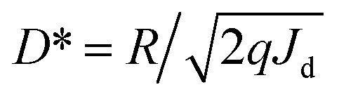 , the D* under zero and a −1 V bias as a function of different wavelengths can be plotted according to the EQE spectra. Fig. 4c shows that the HPDs have a wide spectral range expanding from the visible to the NIR region, achieving over 1011 Jones D* in the visible region and 1010 Jones D* in the NIR region.
3. Conclusions
In conclusion, we report a solution-processed photodetector with a broad spectral range from 300 nm to 1600 nm by applying P3HT:PbS QD BHJ nanocomposites as a photo-active layer. Since P3HT dominates the matrix in the BHJ nanocomposites, an extremely low Jd is achieved due to the large energy barrier for electron injection under reverse bias. In addition, the efficient exciton dissociation at the P3HT:PbS QD interface and long-lived mobile carrier, which were verified by PL and PA measurements, give rise to high Jph of the HPDs under illumination. As a result, detectivities greater than 1011 Jones in the visible region and 1010 Jones in the NIR region were observed. This study provides a simple way to realize uncooled solution-processed broadband PDs with high sensitivity.4. Experimental
4.1. Synthesis of PbS QDs
PbCl2 (1 mmol, 0.28 g) was added to 5 mL of oleylamine (OLA) at room temperature, and the resultant solution was heated to 120 °C under vacuum and was left for 30 minutes under vigorous stirring until the PbCl2–OLA mixture turned into a homogeneous clear solution. Elemental sulfur (0.4 mmol, 14 mg) was dissolved in 2.5 mL of OLA by heating at 80 °C in an oil bath, which gave a deep red solution.35 The resultant sulfur solution was injected into the PbCl2–OLA solution at 140 °C. The resultant mixture was aged at this temperature for 1 hour, resulting in a black colloidal solution. After centrifugation and purification, PbS QDs were synthesized.4.2. Device fabrication
Firstly, the ITO/glass substrates were cleaned by ultrasonication in detergent, de-ionized water, acetone, and isopropanol followed by drying in the incubator. Then, the ITO/glass substrates were treated by UV-ozone for 20 minutes, followed by spin-coating the P3HT:PbS QDs from the dichlorobenzene (o-DCB) solution with a concentration of 10 mg mL−1. Lastly, the HPDs device was completed by thermal deposition of 100 nm Al in the vacuum chamber. The device area is measured to be 0.16 mm2.4.3. Thin film characterization
UV-vis absorption spectra of P3HT, PbS QDs, and P3HT:PbS QD thin films were measured using a HP 8453 spectrophotometer. Measurement of the TEM images of the pristine PbS QD thin film was carried out via a JEOL TEM using an accelerating voltage of 120 kV. Photoluminescence (PL) spectra were obtained using a 532 nm pulsed laser as the excitation source at a frequency of 9.743 MHz. The transient absorption (TA) measurements were carried out using a dual-beam femtosecond spectrometer utilizing the second harmonic of an OPA (optical parametric amplifier) as the pump and a white light continuum as the probe.4.4. Photodetector characterization
The current density–voltage (J–V) characteristics of HPDs were characterized under an AM1.5G calibrated solar simulator (Newport model 91160-1000). The light intensity of the white light was 100 mW cm−2. The light intensity was calibrated by utilizing a mono-silicon detector (with KG-5 visible color filter) of the National Renewable Energy Laboratory to reduce spectral mismatch. The monochromatic light at λ = 500 nm was obtained by placing an optical filter (λ = 500 nm) under the solar simulator. The J–V characteristics were obtained using a Keithley 2400 source meter. The external quantum efficiency (EQE) spectra were measured through the EQE measurement setup in use at ESTI for cells and mini-modules. A 300 W steady-state xenon lamp provides the source light. Up to 64 filters (ranging from 300 to 1600 nm) are available on four filter-wheels to produce the monochromatic input, which is chopped at 75 Hz, superimposed on the bias light, and measured via the usual lock-in technique.Acknowledgements
The authors would like to thank NSF (EECS 1351785) and Air Force Scientific Research (FA9550-15-1-0292) for financial support.References
- A. Rogalski, J. Antoszewski and L. Faraone, J. Appl. Phys., 2009, 105, 091101 CrossRef.
- M. Ettenberg, Adv. Imaging, 2005, 20, 29–33 Search PubMed.
- E. H. Sargent, Adv. Mater., 2005, 17, 515–522 CrossRef CAS.
- S. Kim, Y. T. Lim, E. G. Soltesz, A. M. De Grand, J. Lee, A. Nakayama, J. A. Parker, T. Mihaljevic, R. G. Laurence, D. M. Dor, L. H. Cohn, M. G. Bawendi and J. V. Frangioni, Nat. Biotechnol., 2004, 22, 93–97 CrossRef CAS PubMed.
- H. Sirringhaus, N. Tessler and R. H. Friend, Synth. Met., 1999, 102, 857–860 CrossRef CAS.
- H. Sirringhaus, N. Tessler and R. H. Friend, Science, 1998, 280, 1741–1744 CrossRef CAS PubMed.
- Y. Yang and A. J. Heeger, Appl. Phys. Lett., 1994, 64, 1245–1247 CrossRef CAS.
- H. Sirringhaus, R. J. Wilson, R. H. Friend, M. Inbasekaran, W. Wu, E. P. Woo, M. Grell and D. D. C. Bradley, Appl. Phys. Lett., 2000, 77, 406–408 CrossRef CAS.
- J. Y. Kim, K. Lee, N. E. Coates, D. Moses, T. Q. Nguyen, M. Dante and A. J. Heeger, Science, 2007, 317, 222–225 CrossRef CAS PubMed.
- N. M. Park, T. S. Kim and S. J. Park, Appl. Phys. Lett., 2001, 78, 2575–2577 CrossRef CAS.
- X. Michalet, F. F. Pinaud, L. A. Bentolila, J. M. Tsay, S. J. J. L. Doose, J. J. Li, G. Sundaresan, A. M. Wu, S. S. Gambhir and S. Weiss, Science, 2005, 307, 538–544 CrossRef CAS PubMed.
- D. Pan, E. Towe and S. Kennerly, Appl. Phys. Lett., 1998, 73, 1937–1939 CrossRef CAS.
- G. Konstantatos, I. Howard, A. Fischer, S. Hoogland, J. Clifford, E. Klem, L. Levina and E. H. Sargent, Nature, 2006, 442, 180–183 CrossRef CAS PubMed.
- G. Yu, J. Wang, J. McElvain and A. J. Heeger, Adv. Mater., 1998, 10, 1431–1434 CrossRef CAS.
- P. Peumans, V. Bulovic and S. R. Forrest, Appl. Phys. Lett., 2000, 76, 3855–3857 CrossRef CAS.
- G. A. O'Brien, A. J. Quinn, D. A. Tanner and G. Redmond, Adv. Mater., 2006, 18, 2379–2383 CrossRef.
- X. Gong, M. Tong, Y. Xia, W. Cai, J. S. Moon, Y. Cao, G. Yu, C. L. Shieh, B. Nilsson and A. J. Heeger, Science, 2009, 325, 1665–1667 CrossRef CAS PubMed.
- G. Konstantatos, M. Badioli, L. Gaudreau, J. Osmond, M. Bernechea, F. P. G. De Arquer, F. Gatti and F. H. Koppens, Nat. Nanotechnol., 2012, 7, 363–368 CrossRef CAS PubMed.
- N. S. Sariciftci, L. Simliowitz, F. Wudl and A. J. Heeger, Science, 1992, 258, 1474 CAS.
- R. Mastria, A. Rizzo, C. Giansante, D. Ballarini, L. Dominici, O. Inganäs and G. Gigli, J. Phys. Chem. C, 2015, 119, 14972–14979 CAS.
- S. Kahmann, A. Mura, L. Protesescu, M. V. Kovalenko, C. J. Brabec and M. A. Loi, J. Mater. Chem. C, 2015, 3, 5499–5505 RSC.
- S. A. McDonald, G. Konstantatos, S. Zhang, P. W. Cyr, E. J. Klem, L. Levina and E. H. Sargent, Nat. Mater., 2005, 4, 138–142 CrossRef CAS PubMed.
- X. Jiang, R. D. Schaller, S. B. Lee, J. M. Pietryga, V. I. Klimov and A. A. Zakhidov, J. Mater. Res., 2007, 22, 2204–2210 CrossRef CAS.
- I. Moreels, Y. Justo, B. De Geyter, K. Haustraete, J. C. Martins and Z. Hens, ACS Nano, 2011, 5, 2004–2012 CrossRef CAS PubMed.
- W. U. Huynh, J. J. Dittmer and A. P. Alivisatos, Science, 2002, 295, 2425–2427 CrossRef CAS PubMed.
- S. R. Cowan, A. Roy and A. J. Heeger, Phys. Rev. B: Condens. Matter Mater. Phys., 2010, 82, 245207 CrossRef.
- J. L. Bredas and G. B. Street, Acc. Chem. Res., 1985, 18, 309–315 CrossRef CAS.
- C. Deibel, T. Strobel and V. Dyakonov, Phys. Rev. Lett., 2009, 103, 036402 CrossRef PubMed.
- F. Padinger, R. S. Rittberger and N. S. Sariciftci, Adv. Funct. Mater., 2003, 13, 85–88 CrossRef CAS.
- Y. Kim, S. Cook, S. M. Tuladhar, S. A. Choulis, J. Nelson, J. R. Durrant, D. D. Bradley, M. Giles, I. McCulloch, C. S. Ha and M. Ree, Nat. Mater., 2009, 5, 197–203 CrossRef.
- C. He, C. Zhong, H. Wu, R. Yang, W. Yang, F. Huang, G. C. Bazan and Y. Cao, J. Mater. Chem., 2010, 20, 2617–2622 RSC.
- L. Li, F. Zhang, W. Wang, Q. An, J. Wang, Q. Sun and M. Zhang, ACS Appl. Mater. Interfaces, 2015, 7, 5890–5897 CAS.
- M. C. Scharber, D. Muhlbacher, M. Koppe, P. Denk, C. Waldauf, A. J. Heeger and C. J. Brabec, Adv. Mater., 2006, 18, 789–794 CrossRef CAS.
- C. J. Brabec, A. Cravino, D. Meissner, N. S. Sariciftci, T. Fromherz, M. T. Rispens, L. Sanchez and J. C. Hummelen, Adv. Funct. Mater., 2010, 11, 374–380 CrossRef.
- L. Bakueva, I. Gorelikov, S. Musikhin, X. S. Zhao, E. H. Sargent and E. Kumacheva, Adv. Mater., 2004, 16, 926–929 CrossRef CAS.
| This journal is © The Royal Society of Chemistry 2017 |