
 Open Access Article
 This Open Access Article is licensed under a Creative Commons Attribution-Non Commercial 3.0 Unported Licence
Experimental and theoretical investigations on the defect and optical properties of S- and Al-doped GaSe crystals
Changbao Huang ,
Zhenyou Wang,
Youbao Ni,
Haixin Wu* and
Shijing Chen
,
Zhenyou Wang,
Youbao Ni,
Haixin Wu* and
Shijing Chen
Anhui Provincial Key Laboratory of Photonic Devices and Materials, Anhui Institute of Optics and Fine Mechanics, Chinese Academy of Sciences, Hefei 230031, China. E-mail: hxwu@aiofm.ac.cn
First published on 28th April 2017
Abstract
A combination of experimental and computational methods was performed to investigate the defect and optical properties of S-doped and Al-doped GaSe crystals. Our experimental and calculated results indicate that the doped S and Al atoms can form SSe and AlGa+ substitutional defects in the layered GaSe structure. The non-isovalent AlGa+ defect can strengthen the chemical bonding within the intralayer and induce complex defects within the interlayer in the layered GaSe structure. Al-doping maximally improves the hardness of GaSe, which makes it a promising nonlinear frequency conversion material in the infrared and THz ranges. The isovalent SSe defect determines the GaSe1−xSx mixed structure. Calculated results indicate that the refractive index of GaSe1−xSx decreases with the x value, while the band gap increases. The unique properties of GaSe1−xSx may make it a potential candidate for double heterojunction photoelectric materials.
Introduction
Layered III–VI materials, such as GaSe, GaS, InSe and GaTe, have attracted increasing interest in photoelectronic devices due to their exotic electronic and optical properties.1–4 GaSe is a typical layered III–VI material. Each layer of GaSe has hexagonal symmetry and is composed of four atomic Se–Ga–Ga–Se sheets with intralayer covalent bond connections, while interlayer bonds are of weak van der Waals type.5 Triggered by the discovery of the two-dimensional graphene,6 the GaSe monolayers have been investigated as quasi-two-dimensional (2D) materials. On the basis of first-principles density functional theory (DFT) calculations, the electronic4,7–9 and magnetic properties10,11 were studied to explore their promising applications in field-effect transistors, heterostructures and spintronics devices. Experimentally, the GaSe monolayers have been fabricated by using micromechanical12 and van der Waals (vdW) epitaxy techniques,3 and graphene–GaSe dual heterojunction13 and GaS–GaSe field-effect transistors14 have been successfully fabricated. Moreover, due to their excellent optical performances, such as large nonlinear coefficient (75 pm/V) and birefringence (0.34), wide transparency range (0.62–18 μm) and high damage threshold, GaSe crystals have been used to generate coherent lasers in a wide spectral range from the IR to THz regions by nonlinear frequency conversion (NFC).15–17It is well known that the layered GaSe structure can well incorporate different doped elements. Different elements doping have been performed to modify or manipulate the mechanical, optical, electronic, magnetic and electrical properties of GaSe.18–24 Among these incorporated elements, S- and Al-doping have great attractions. The S-doping allows for control of the electronic, optical properties and lattice strengthening of GaSe within wide ranges.20,25,26 Moreover, the GaS–GaSe show possibilities in applications of field-effect transistors, photodetectors and photocatalysts.7,8,14,27 The Al-doping could maximumly improve the microhardness of GaSe crystal, which makes is as promising NFC materials in the IR and THz range.18–20,28 However, the lower concentration Al-doping (0.5 at%) resulted in the degradation of its optical quality.
The intrinsic and extrinsic defects, which can modify or spoil the performance of materials, play an important role in host structure. It is thus desirable to study the defect information of the doped GaSe in detail. It was experimentally observed that the non-isovalent doped GaSe usually shown deep-level and defect complexes.24,29,30 Even the Ga excess condition,31 isovalent Te-doping32 and In-doping33,34 in GaSe structure, could form interstitial defects and create donor–acceptor (D–A) pair level of defect complexes. The present work focuses on the experimental and theoretical studies on the defect properties of S-doped and Al-doped GaSe crystals. Based on the results of defect studies, the crystal performances were characterized and predicted by using experimental and theoretical methods.
Experimental and theoretical method
Experimental characterization
Single crystals of pure, S-doped GaSe and Al-doped GaSe were grown by using Bridgman method. The samples were prepared by cleaving or cutting an ingot along (0001) face. The surface topography of these samples was observed by using a Hitachi SU-8020 scanning electron microscope (SEM) instrument. Raman spectra were recorded by a Raman-Fourier spectrometer LabRam HR Evolution (HORIBA JOBIN YVON) within: Δλ = 3200–50 cm−1 with spectral resolution 0.05 cm−1 and 785 nm laser pump. The photoluminescence (PL) measurements were done at 78 K by immersing the samples in liquid nitrogen. A semiconductor laser operating at a wavelength 532 nm was used as a source of excitation. The intensity of the laser beam was 0.02% × 60 mW μm−2. The chemical states of each element in the samples were examined by X-ray photoelectron spectra (XPS) using a Thermo Scientific Escalab 250Xi instrument equipped with a monochromatic Al Kα X-ray source and a hemispherical analyzer. Appropriate electronic charge compensation was employed to perform the analysis and binding energy was referenced to the C-1s peak.Theoretical calculations
To further understand the defect properties in GaSe system, we performed the first-principles calculations. For this purpose we used density functional theory (DFT) implemented in Quantum ESPRESSO package.35 The effective ionic potentials36 were approximated by projector-augmented wave (PAW) method and the valence electron configurations are Ga(3d4s4p), Se(4s4p), S(3s4p) and Al(3s3p). The exchange–correlation energy of electrons was evaluated in the local density approach (LDA) within the Perdew–Wang scheme.37 The Brillouin-zone integrations were performed using special k-point sampling of the Monkhorst-Pack scheme. In all calculations, a 114 Ry energy cutoff and 5 × 5 × 3 k-points were used for the 3 × 3 × 1 virgin and defective supercell, which guaranteed the convergence within 0.0002 Ry for total energy. All the structures were relaxed to minimize the total energy of the systems until the residual forces fell below 0.002 eV A−1.Results and discussions
Experimental analysis
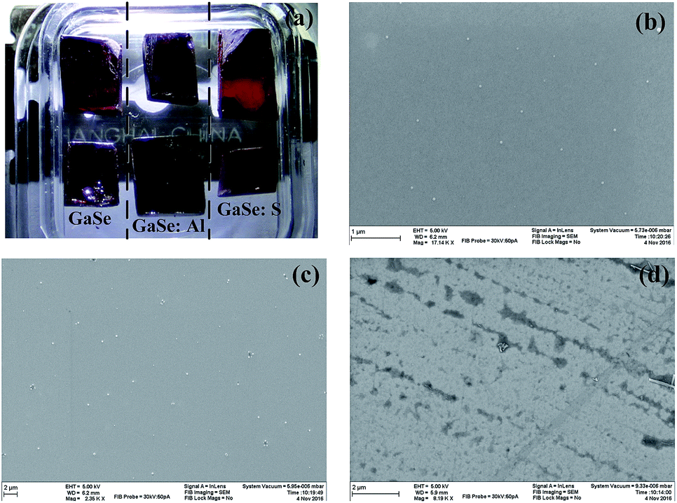 | ||
| Fig. 1 (a) Photograph of single crystal samples; SEM pictures with ten micrometer size of (b) pure, (c) S-doped (2.3 wt%) and (d) Al-doped (0.23 wt%) GaSe crystal samples. | ||
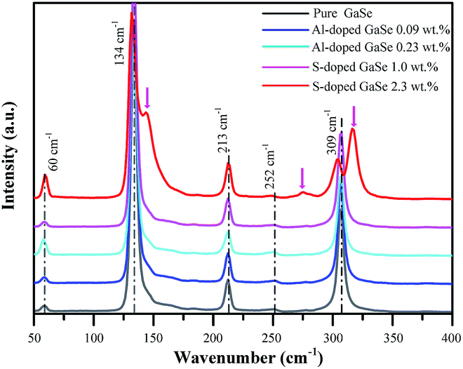 | ||
| Fig. 2 Raman spectra of pure, S-doped (1.0, 2.3 wt%) and Al-doped (0.09, 0.23 wt%) GaSe crystal samples. | ||
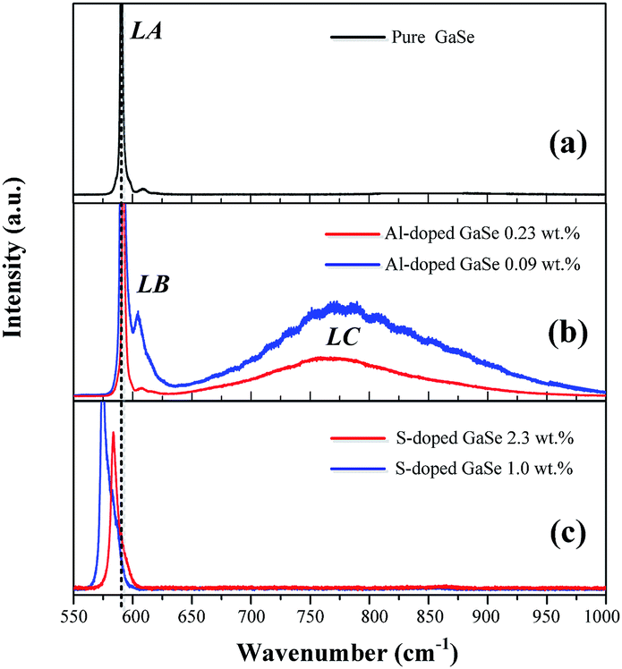 | ||
| Fig. 3 PL spectra of (a) pure, (b) S-doped (1.0, 2.3 wt%) and (c) Al-doped (0.09, 0.23 wt%) GaSe crystals at 78 K. | ||
The Al ion has charge of plus three in stable Al2Se3 compound, while Ga ion forms (Ga–Ga)4+ dimer unit in the GaSe.5 Therefore, the Al atoms embed in GaSe layer structure as substitutional defect AlGa1+ or interstitial defect Ali3+. The positive centers AlGa1+ may induce compensation defects of VGa2− or Sei2− and form defect complexes in the GaSe structure. The densities of the defect complexes increase with Al-doping concentrations, which leads to the strengthening of LB and LC band as mentioned above. Both GaS and GaSe have the same layer structure and valence states of elements. Doped with S, the positions of Se atoms are occupied by S atoms, and the SSe defect is non-radiative centers. The shifting and widening of LA band in S-doped sample may be induced by the non-coincidence of covalent radii and electron affinity between S atom and Se atoms. This explains why the S-doping has high concentrations in GaSe structure.
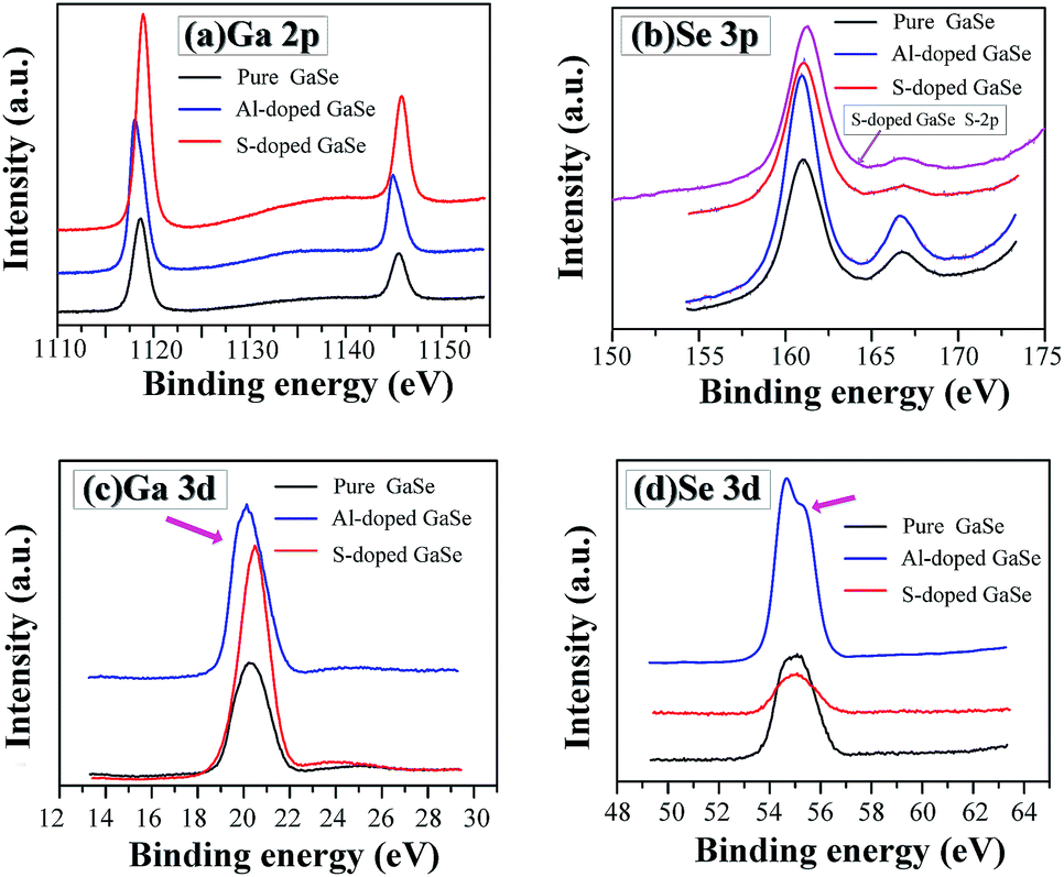 | ||
| Fig. 4 XPS spectra of (a) Ga-2p, (b) Se-3p, (c) Ga-3d and (d) Se-3d in the pure, S-doped (2.3 wt%) and Al-doped (0.23 wt%) GaSe crystal samples. | ||
It is noted that trace amounts of Al atoms cannot be detected by XPS in the 0.23 wt% Al-doped sample. However, the effects of Al-doping on chemical states in the GaSe structure can be observed from the Se-3d and Ga-3d XPS spectra. Usually, the 3d5/2 and 3d3/2 peaks of Ga and Se atoms do not split in GaSe crystal.39 For the pure and S-doped samples, the 3d peaks (Fig. 4c and d) of Ga and Se atoms preserve the basic symmetry, which are identical to those of unoxidized GaSe reported in ref. 39 and 40. For the Al-doped sample, the Se-3d peak demonstrates the obvious dissymmetry and can be resolved into two overlapping peaks. This may be due to the changes of Se chemical states. On one hand, the substitution of Al3+ on one ion of (Ga–Ga)4+ dimer units leads to a change of valence state of Se. On the other hand, the interlayer interstitial atoms form chemical bonding with Se atom in the layer structure of GaSe. The mixed valent Se may result in the dissymmetry or separation of Se-3d XPS peak in the Al-doped sample. As with the influence of oxidation states of Ga (Ga2O3) on Ga-3d state in GaSe structure,39 the substitutions of AlGa1+ may induce the change of Ga chemical state, from Ga2+ to Ga3+, and result in the slight dissymmetry of Ga-3d XPS peak (Fig. 4c).
Calculated results
Formation energy
We describe the formation energies of different defects to find out which defect is more likely to be present in doped GaSe. The formation energy of a defect D in charge state q is defined as41
 | (1) |
The chemical potential μX = μelemX + ΔμX, is restricted by the following equilibrium conditions: ΔμGa + ΔμSe = ΔGf(GaSe) to maintain a stable compound; ΔμGa + ΔμS ≤ ΔGf(GaS) and 3ΔμAl + 2ΔμSe ≤ ΔGf(Al2Se3) to avoid the formation of secondary phases between the host elements and impurities; ΔμAl and ΔμS ≤ 0 to prevent precipitation of the elemental solids (S or Al). Here ΔGf is the calculated Gibbs energy of formation: ΔGf(GaSe) = −1.17 eV (which is closed to other theoretical value −1.12 eV (ref. 34)), ΔGf(GaS) = −1.36 eV and ΔGf(Al2Se3) = −0.60 eV. For GaSe under Se-rich (Ga-poor) condition, ΔμGa and ΔμSe are equal to 0 eV and −1.17 eV respectively; under Ga-rich (Se-poor), ΔμGa and ΔμSe are equal to −1.17 eV and 0 eV respectively. The thermodynamic transition level ε(q1/q2) is defined as the Fermi-level position for which the formation energies of charge states q1 and q2 are equal:
 | (2) |
Although the LDA can successfully predict the ground-states properties of semiconductors, the shortcoming of LDA leads to the underestimations of energy gaps or Fermi-levels of semiconductors. Presently, the Fermi-level is set between 0 and experimental energy gap (2.12 eV at 77 K (ref. 38)). Schematic diagrams of the defect formation energies as a function of the Fermi-level position and for stable charge-states q are shown in Fig. 5. From the trend of the calculated formation energy in pure, S-doped and Al-doped GaSe, we found the following conclusions:
 | ||
| Fig. 5 Schematic diagrams of the formation energies Ef as a function of the Fermi-level EF position and for stable charge-states q. Ef of (a) and (b) intrinsic defects, (c) and (d) Al impurity, (e) and (f) S impurity under Ga-rich and Se-rich conditions, respectively. | ||
Electronic properties
Supercell calculations produce folding and complicated electronic band structure (EBS), which makes it difficult to assess the influence of defect perturbations on the EBS of GaSe. In this work, we unfolded the EBS of defective supercell into that of primitive cell (PC) by using BandUp code.43,44 Fig. 6 shows the EBS for the case of the (a) SSe and (b) AlGa_VGa systems. The color scale represent the number of PC bands crossing, which depends on the Bloch state of wave vector ki and eigenvalue εi.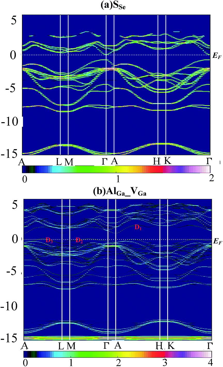 | ||
| Fig. 6 Electronic band structure of supercell unfolded by using BandUp code: (a) SSe and (b) AlGa_VGa system. | ||
The orbital character of SSe supercell (Fig. 6a) is similar to these of virgin supercell and GaSe PC which has been described in ref. 38.
In order to understand the nature of SSe defect further, we plot the project density of states (DOS) of S and Se atom in SSe system, as shown in Fig. 7a. Despite the large different in radius and electro-negativity between S and Se atoms, a good match between the orbitals of isovalent S and Se ions produces the similar EBS of SSe system with that of pristine GaSe, which is in accordance with the measured results of XPS. The S-doping does not induce new defect states in the band gap, but increases the band gap value.
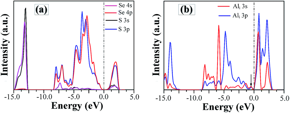 | ||
| Fig. 7 The project density of states of (a) S and Se atoms in SSe system and (b) Al atom in Ali system. | ||
Compared to the pristine GaSe EBS, the PC eigenvalues are smeared by the embed defects in AlGa_VGa defective system. Moreover, the AlGa_VGa defects make the Femi-level move downward in the VGa system. There are three new states appear in the gap: D1 above and D2, D3 below Femi-level. The unoccupied defect state of D1 may come from the conduction band formed out of Se-p orbitals, while D2 and D3 may split off from the rest of the valence bands. Moreover, the defect state induced by interstitial defect Ali is located in the gap, as shown in Fig. 7b.
Crystal performances
In layer GaSe structure, the cation–cation bonds are along the z crystallographic axes and at about 120-degree angle to cation–anion bonds. As shown in Fig. 8, the S-doping and Al-doping decrease the bonding length in the hexagonal units. The incorporations of S and Al atoms could strengthen the intralayer chemical bonding of layer GaSe structure and improve its micro-hardness. Moreover, the new chemical bonds between interlayer formed by Ali3+ defect can strengthen the interlayer force and further improve the mechanical performance of GaSe crystal. The calculated results demonstrate that the Se-rich condition is good for the growth of Al-doped GaSe crystals. By using modified Bridgman method with Se-rich condition, we have successfully grown large size Ga0.49Se0.50:0.15 wt% Al (Fig. 9a) and Ga0.49Se0.50:0.35 wt% Al (Fig. 9b) single crystals, which possess indentation hardness of 2.27 GPa and 2.79 GPa, respectively, compared to 0.87 GPa of pure GaSe crystal. The Ga0.49Se0.50:0.35 wt% Al sample can be cut and polished with any orientation, as shown in Fig. 9b. However, the higher concentration Al-doping may produce the complex defect associations and spoil the optical performance of GaSe (Fig. 9c).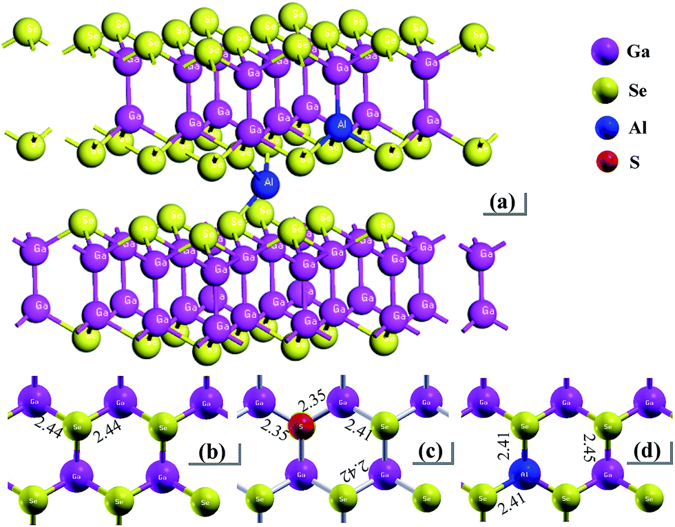 | ||
| Fig. 8 Schematic view of (a) Al-doped GaSe system including Al3+ interstitial defect and AlGa defect, and plan view and bonding length of a layer in (b) virgin, (c) SSe and (d) AlGa systems. | ||
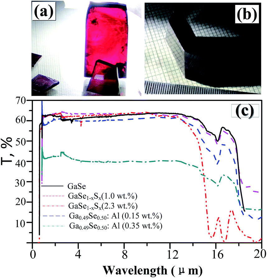 | ||
| Fig. 9 (a) Ga0.49Se0.50:0.15 wt% Al and (b) Ga0.49Se0.50:0.35 wt% Al single crystal samples. (c) Full range transparency spectra in infrared range of pure and doped GaSe crystal. | ||
The frequency dependent dielectric permittivity can be described as follow:
 | (3) |
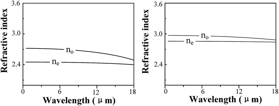 | ||
| Fig. 10 Refractive indexes of (a) GaS and (b) GaSe calculated by using the DFPT method. | ||
Conclusions
A combination of experimental and computational methods was performed to investigate the defect and optical properties of S-doped and Al-doped GaSe crystals. The measurements of PL, XPS and SEM indicate that S atoms form SSe substitutional defect, and Al atoms could induce complex defects of AlGa+ and the interlayer interstitial atoms. Results of defect formation energy calculations are in accordance with experimental measurements for the doped defect types. The calculations of electronic properties (EBS and DOS) reveal the defect levels of Al-doped systems. Moreover, the calculated results indicate that the Se-rich condition is good for the growth of Al-doped GaSe crystals. Based on these calculations, we successfully grown Al-doped GaSe crystals with higher hardness and optical quality. Attracted by the layer GaSe1−xSx mixture structure, we investigate its dielectric properties by using DFPT, which reveals that the refractive index of GaSe1−xSx decreases with x value.The significantly improved hardness of Al-doped GaSe crystal make it more propitious to be cut and polished with specific orientation for use, which could improve the laser conversion efficiency. Therefore, the Al-doped GaSe crystal can be used as promising nonlinear frequency conversion materials in the infrared and THz ranges. The energy gap and refractive index of GaSe1−xSx can be controlled by adjusting S-doping concentrations. The unique properties of GaSe1−xSx may make it a potential candidate for the double heterojunction photoelectric material.
Acknowledgements
The authors acknowledge financial support from Knowledge Innovation Program of the Chinese Academy of Sciences (CXJJ-16M128). Part of the calculations was performed in Center for Computational Science of CASHIPS. The atomic structures are visualized using the XCrysDen code.46 We used the pseudopotentials from the Quantum ESPRESSO pseudopotential data base: http://www.quantum-espresso.org/pseudopotentials.References
- K. R. Allakhverdiev, M. Ö. Yetis, S. Ozbek, T. K. Baykara and E. Y. Salaev, Laser Phys., 2009, 19, 1092–1104 CrossRef CAS.
- Y. Tang, K. C. Mandal, J. A. McGuire and C. W. Lai, Phys. Rev. B, 2016, 94, 125302 CrossRef.
- H. Cai, E. Soignard, C. Ataca, B. Chen, C. Ko, T. Aoki, A. Pant, X. Meng, S. Yang, J. Grossman, F. D. Ogletree and S. Tongay, Adv. Mater., 2016, 28, 7375–7382 CrossRef CAS PubMed.
- D. V. Rybkovskiy, A. V. Osadchy and E. D. Obraztsova, Phys. Rev. B: Condens. Matter Mater. Phys., 2014, 90, 235302 CrossRef.
- N. C. Fernelius, Prog. Cryst. Growth Charact. Mater., 1994, 28, 275–353 CrossRef CAS.
- K. S. Novoselov, A. K. Geim, S. V. Morozov, D. Jiang, Y. Zhang, S. V. Dubonos, I. V. Grigorieva and A. A. Firsov, Science, 2004, 306, 666–669 CrossRef CAS PubMed.
- W. Wei, Y. Dai, C. Niu, X. Li, Y. Ma and B. Huang, J. Mater. Chem. C, 2015, 3, 11548–11554 RSC.
- Y. Ma, Y. Dai, M. Guo, L. Yu and B. Huang, Phys. Chem. Chem. Phys., 2013, 15, 7098–7105 RSC.
- D. V. Rybkovskiy, N. R. Arutyunyan, A. S. Orekhov, I. A. Gromchenko, I. V. Vorobiev, A. V. Osadchy, E. Y. Salaev, T. K. Baykara, K. R. Allakhverdiev and E. D. Obraztsova, Phys. Rev. B: Condens. Matter Mater. Phys., 2011, 84, 085314 CrossRef.
- L. Ao, H. Y. Xiao, X. Xiang, S. Li, K. Z. Liu, H. Huang and X. T. Zu, Phys. Chem. Chem. Phys., 2015, 17, 10737–10748 RSC.
- T. Cao, Z. Li and S. G. Louie, Phys. Rev. Lett., 2015, 114, 236602 CrossRef PubMed.
- L. Quan, Y. Song, Y. Lin, G. Zhang, Y. Dai, Y. Wu, K. Jin, H. Ding, N. Pan, Y. Luo and X. Wang, J. Mater. Chem. C, 2015, 3, 11129–11134 RSC.
- W. Kim, C. Li, F. A. Chaves, D. Jimenez, R. D. Rodriguez, J. Susoma, M. A. Fenner, H. Lipsanen and J. Riikonen, Adv. Mater., 2016, 28, 1845–1852 CrossRef CAS PubMed.
- D. J. Late, B. Liu, J. Luo, A. Yan, H. S. S. R. Matte, M. Grayson, C. N. R. Rao and V. P. Dravid, Adv. Mater., 2012, 24, 3549–3554 CrossRef CAS PubMed.
- W. Shi, Y. J. Ding, X. Mu and N. Fernelius, Appl. Phys. Lett., 2002, 80, 3889 CrossRef CAS.
- Z. Rao, X. Wang and Y. Lu, Opt. Commun., 2011, 284, 5472–5474 CrossRef CAS.
- K. Finsterbusch, A. Bayer and H. Zacharias, Appl. Phys. B, 2004, 79, 457–462 CrossRef CAS.
- Y.-F. Zhang, R. Wang, Z.-H. Kang, L.-L. Qu, Y. Jiang, J.-Y. Gao, Y. M. Andreev, G. V. Lanskii, K. A. Kokh, A. N. Morozov, A. V. Shaiduko and V. V. Zuev, Opt. Commun., 2011, 284, 1677–1681 CrossRef CAS.
- J. Guo, J. J. Xie, L. M. Zhang, D. J. Li, G. L. Yang, Y. M. Andreev, K. A. Kokh, G. V. Lanskii, A. V. Shabalina, A. V. Shaiduko and V. A. Svetlichnyi, CrystEngComm, 2013, 15, 6323 RSC.
- J. Guo, J.-J. Xie, D.-J. Li, G.-L. Yang, F. Chen, C.-R. Wang, L.-M. Zhang, Y. M. Andreev, K. A. Kokh, G. V. Lanskii and V. A. Svetlichnyi, Light: Sci. Appl., 2015, 4, e362 CrossRef CAS.
- Z. S. Feng, J. Guo, J. J. Xie, L. M. Zhang, J. Y. Gao, Y. M. Andreev, T. I. Izaak, K. A. Kokh, G. V. Lanskii, A. V. Shaiduko, A. V. Shabalina and V. A. Svetlichnyi, Opt. Commun., 2014, 318, 205–211 CrossRef CAS.
- Z. S. Feng, Z. H. Kang, F. G. Wu, J. Y. Gao, Y. Jiang, H. Z. Zhang, Y. M. Andreev, G. V. Lanskii, V. V. Atuchin and T. A. Gavrilova, Opt. Express, 2008, 16, 9978–9985 CrossRef CAS PubMed.
- M. Yüksek, A. Elmali, M. Karabulut and G. M. Mamedov, Opt. Mater., 2009, 31, 1663–1666 CrossRef.
- Y.-K. Hsu, C.-S. Chang and W.-C. Huang, J. Appl. Phys., 2004, 96, 1563 CrossRef CAS.
- K. A. Kokh, J. F. Molloy, M. Naftaly, Y. Andreev, V. A. Svetlichnyi, G. V. Lanskii, I. N. Lapin, T. I. Izaak and A. E. Kokh, Mater. Chem. Phys., 2015, 154, 152–157 CrossRef CAS.
- Y. M. Andreev, V. V. Atuchin, G. V. Lanskii, A. N. Morozov, L. D. Pokrovsky, S. Y. Sarkisov and O. V. Voevodina, Mater. Sci. Eng. B, 2006, 128, 205–210 CrossRef CAS.
- C. S. Jung, K. Park, F. Shojaei, J. Y. Oh, H. S. Im, J. A. Lee, D. M. Jang, J. Park, N. Myoung, C.-L. Lee, J. W. Lee, J. K. Song and H. S. Kang, Chem. Mater., 2016, 28, 5811–5820 CrossRef CAS.
- S. Das, C. Ghosh, O. G. Voevodina, Y. M. Andreev and S. Y. Sarkisov, Appl. Phys. B, 2005, 82, 43–46 CrossRef.
- S. Shigetomi, T. Ikari and H. Nakashima, J. Appl. Phys., 1993, 74, 4125–4129 CrossRef CAS.
- S. Shigetomi, T. Ikari and H. Nakashima, J. Appl. Phys., 1996, 80, 4779–4781 CrossRef CAS.
- S. Shigetomi and T. Ikari, J. Appl. Phys., 2003, 94, 5399–5401 CrossRef CAS.
- I. Evtodiev, L. Leontie, M. Caraman, M. Stamate and E. Arama, J. Appl. Phys., 2009, 105, 023524 CrossRef.
- Y. Cui, R. Dupere, A. Burger, D. Johnstone, K. C. Mandal and S. A. Payne, J. Appl. Phys., 2008, 103, 013710 CrossRef.
- Z. Rak, S. D. Mahanti, K. C. Mandal and N. C. Fernelius, Phys. Rev. B: Condens. Matter Mater. Phys., 2010, 82, 155203 CrossRef.
- P. Giannozzi, S. Baroni, N. Bonini, M. Calandra, R. Car, C. Cavazzoni, D. Ceresoli, G. L. Chiarotti, M. Cococcioni, I. Dabo, A. Dal Corso, S. de Gironcoli, S. Fabris, G. Fratesi, R. Gebauer, U. Gerstmann, C. Gougoussis, A. Kokalj, M. Lazzeri, L. Martin-Samos, N. Marzari, F. Mauri, R. Mazzarello, S. Paolini, A. Pasquarello, L. Paulatto, C. Sbraccia, S. Scandolo, G. Sclauzero, A. P. Seitsonen, A. Smogunov, P. Umari and R. M. Wentzcovitch, J. Phys.: Condens. Matter, 2009, 21, 395502 CrossRef PubMed.
- N. Troullier and J. L. Martins, Phys. Rev. B: Condens. Matter Mater. Phys., 1991, 43, 1993–2006 CrossRef CAS.
- J. P. Perdew and Y. Wang, Phys. Rev. B: Condens. Matter Mater. Phys., 1992, 45, 13244–13249 CrossRef.
- Z. Rak, S. D. Mahanti, K. C. Mandal and N. C. Fernelius, J. Phys. Chem. Solids, 2009, 70, 344–355 CrossRef CAS.
- S. M. Tan, C. K. Chua, D. Sedmidubsky, Z. Sofer and M. Pumera, Phys. Chem. Chem. Phys., 2016, 18, 1699–1711 RSC.
- F. Marquez, A. Segura, V. Munoz and G. Gonzalez, Surf. Interface Anal., 2002, 34, 460–463 CrossRef CAS.
- C. Freysoldt, B. Grabowski, T. Hickel, J. Neugebauer, G. Kresse, A. Janotti and C. G. Van de Walle, Rev. Mod. Phys., 2014, 86, 253–305 CrossRef.
- T. Onai, Y. Nagai, H. Dezaki and Y. Oyama, J. Cryst. Growth, 2013, 380, 18–22 CrossRef CAS.
- P. V. C. Medeiros, S. S. Tsirkin, S. Stafström and J. Björk, Phys. Rev. B: Condens. Matter Mater. Phys., 2015, 91, 041116 CrossRef.
- P. V. C. Medeiros, S. Stafström and J. Björk, Phys. Rev. B: Condens. Matter Mater. Phys., 2014, 89, 041407 CrossRef.
- M. Veithen, X. Gonze and P. Ghosez, Phys. Rev. B: Condens. Matter Mater. Phys., 2005, 71, 125107 CrossRef.
- A. Kokalj, J. Mol. Graphics Modell., 1999, 17, 176–179 CrossRef CAS PubMed.
| This journal is © The Royal Society of Chemistry 2017 |