
 Open Access Article
 This Open Access Article is licensed under a
 Creative Commons Attribution 3.0 Unported Licence
Stabilization of the thermal decomposition process of self-reducible copper ion ink for direct printed conductive patterns†
Kuan-Ming Huanga,
Hiroki Tsukamotob,
Yingqiong Yongb,
Hsien-Lung Chiua,
Mai Thanh Nguyenb,
Tetsu Yonezawa *b and
Ying-Chih Liao*a
*b and
Ying-Chih Liao*a
aDepartment of Chemical Engineering, National Taiwan University, Taipei, Taiwan. E-mail: liaoy@ntu.edu.tw
bDivision of Materials Science and Engineering, Hokkaido University, Sapporo, Hokkaido, Japan. E-mail: tetsu@eng.hokudai.ac.jp
First published on 10th May 2017
Abstract
In this study, a thermally triggered self-reducible copper ink is developed to print conductive patterns on flexible substrates. Inks containing only copper formate (CuF) and monoisopropanol amine (MIPA) generated large bubbles in the CuF decomposing process, and thus the surface morphologies of prepared thin films were largely disturbed. With the addition of octylamine (OA), the bubbling disturbance was relieved due to the lower surface tension and the film uniformity was greatly improved. A low resistivity of 2 × 10⁻⁷ Ω m (8.5% of bulk copper) can be reached by heating the ink at 140 °C for 5 minutes under a nitrogen environment. XRD results showed the synthesized copper films were comprised of pure metallic copper crystalline. The copper films were composed of closely packed spherical grains of 50 to 500 nm in diameter. After the addition of 1 wt% polyvinylpyrrolidone (PVP) in the ink, the synthesized copper thin films showed great adhesion on glass substrates, and sustained the same conductivity after repeated tape tests. The ink can also be printed on flexible substrates, such as polyethylene terephthalate (PET) or polyimide (PI) thin films, to create highly-conductive tracks with a strong mechanical stability. Finally, various conductive patterns were printed on flexible substrates to show the great potential of this ink for various printed electronic applications.
Introduction
The recent advancements in printing technology have provided a new fabrication method for flexible and light-weight electronic devices at low costs. To fabricate these so-called printed electronic devices, inks containing conductive materials are printed on plastic sheets to produce flexible microelectronic circuits. As the most essential part in every circuit, electrically conductive interconnects from metal inks have been widely used in these printed devices. To reduce the manufacturing cost, copper has recently attracted wide attention for printed conductive features because of its low price, and high electric conductivity. The most commonly used copper inks are nanoparticle suspensions.1–7 The printed patterns can yield a low resistivity down to 2.2 times of that for bulk copper2 after sintering at 200 °C for an hour. However, most plastic substrates might melt or deform at this high temperature. Alternatively, electroless plating approach offers a low-temperature synthetic route for copper thin film fabrication on plastic surfaces.8–11 Solutions containing active agents are first printed with micro-contact12–14 or inkjet printing15–20 methods to produce patterns on plastic substrates. Copper metal are then deposited selectively on the printed patterns in a subsequent electroless plating bath.12,13,15,16,19 Although electroless plating methods can produce highly conductive copper thin films on flexible substrates at low temperatures, the method needs two processing steps and the plating fluid might contaminate or modify the plastic surfaces other than the patterned area. Thus, copper inks that can directly print on selected area with low sintering temperatures are still needed for metal interconnects on plastic substrates.To meet the low-temperature sintering and direct writing requirements, metallo–organic decomposition (MOD)21–25 inks currently catch widespread research interests for copper metal pattern formation on plastic substrates. Among all the organic copper salts, copper formate (CuF) is the most commonly used material due to its self-reducible characteristic.26,27 When heated at ∼200 °C, CuF can decompose into copper metal.27–29 To lower the decomposition temperature, CuF is usually mixed with complexing agents, such as alkylamines30,31 or pyridine derivatives.32 These organic copper complexes can decompose at temperatures as low as 100 °C.32,33 Moreover, with a low sintering temperature, one can also print the copper MOD ink on plastic sheets to make flexible conductive patterns.28 These frontier studies have shown great feasibility of copper MOD ink formulation for conductive copper thin films. However, although those copper complexes can decompose into metals at low temperatures, the copper MOD inks are regularly found to have strong dewetting29 or surface morphological problems32 during the thermal calcination process. The non-uniform thickness or distorted boundaries can lead to bad printing quality for precise conductive pattern formation. Moreover, CO2 bubbles generated in CuF decomposition process can also lead to porous nanostructures in the copper films and thus deteriorate the electrical conductivity.33 Generally, these morphological problems can be mitigated by adding copper particles in MOD ink to increase the copper load33,34 or blending two types of amines to control the morphology of the films.29,35 However, the cause of morphological problem is still unsolved and needs detail investigation. Besides morphological problems, the adhesion and mechanical strength of the copper thin films from MOD inks on plastic substrates are also important issues for flexible electronic applications. More investigations on ink surface properties or ink formulations are necessary to address these challenges.
In this work, we aim to formulate a particle-free self-reductive copper ink with low sintering temperature for printed conductive patterns on flexible substrates. Monoisopropanol amine (MIPA) was used to form complex with CuF because of the low thermal decomposition temperature (∼100 °C).33 However, the MIPA–CuF ink dewets easily on glass or plastic surfaces and results in bad printing or coating quality. The cause of morphological problem will be investigated and the morphology of thin films after sintering copper formate ink will be carefully studied to optimize the smoothness and conductivity of the resulting copper thin films. The adhesion of the copper thin films will also be enhanced by addition of binder polymers. The mechanical strength of printed conductive tracks on plastic sheets under bending conditions will also be evaluated, and several examples will be demonstrated to show the potential applications of this ink for printed electronics.
Experimental section
Copper(II) formate tetra-hydrate (Cu(HCOO)2·4H2O, CuF, Wako, Japan) was mixed with monoisopropanol amine (1-amino-2-propanol, MIPA, Junsei, Japan) at a 1![[thin space (1/6-em)]](https://www.rsc.org/images/entities/char_2009.gif) :1 molar ratio to prepare the copper complex. The mixture was strongly mixed with a conditioning mixer to produce CuF–MIPA ink. Octylamine (OA, Kanto Chemical Co., Japan) was then added to CuF–MIPA ink and mixed with a conditioning mixer to produce CuF–MIPA–OA ink. Polyvinylpyrrolidone (PVP, MW 10000, Tokyo Kasei Co., Japan) was added to the ink to promote film printability and adhesion on substrate. All the prepared inks showed deep blue color without any sediments (Fig. S1†). Flexible poly(ethylene terephthalate) (PET, Universal film, Japan) and polyimide (PI, Chang Chun Plastics Co., Ltd., Taiwan) slides were cleaned by rinsing sequentially with deionized water and ethanol. These flexible substrates were then dried in a vacuum oven before used. The printed inks were calcined under a nitrogen environment. The microstructures of the sintered copper thin films and printed samples were examined with scanning electron microscopy (SEM) using a JEOL JSM-6701F field-emission-type SEM. The thicknesses of the copper films were estimated from the cross-sectional SEM images to calculate the resistivity of the copper films. X-ray diffraction (XRD) patterns were collected using a Rigaku Miniflex-II diffractometer. Thermogravimetric differential thermal analysis (TG-DTA) was performed using a Shimadzu DTG-60H to study the decomposition of CuF–MIPA and CuF–MIPA–OA inks. The sheet resistances of the sintered copper films were measured by using a resistivity meters (Mitsubishi Chemical Analytech Loresta-GP) at four-point probe mode.
:1 molar ratio to prepare the copper complex. The mixture was strongly mixed with a conditioning mixer to produce CuF–MIPA ink. Octylamine (OA, Kanto Chemical Co., Japan) was then added to CuF–MIPA ink and mixed with a conditioning mixer to produce CuF–MIPA–OA ink. Polyvinylpyrrolidone (PVP, MW 10000, Tokyo Kasei Co., Japan) was added to the ink to promote film printability and adhesion on substrate. All the prepared inks showed deep blue color without any sediments (Fig. S1†). Flexible poly(ethylene terephthalate) (PET, Universal film, Japan) and polyimide (PI, Chang Chun Plastics Co., Ltd., Taiwan) slides were cleaned by rinsing sequentially with deionized water and ethanol. These flexible substrates were then dried in a vacuum oven before used. The printed inks were calcined under a nitrogen environment. The microstructures of the sintered copper thin films and printed samples were examined with scanning electron microscopy (SEM) using a JEOL JSM-6701F field-emission-type SEM. The thicknesses of the copper films were estimated from the cross-sectional SEM images to calculate the resistivity of the copper films. X-ray diffraction (XRD) patterns were collected using a Rigaku Miniflex-II diffractometer. Thermogravimetric differential thermal analysis (TG-DTA) was performed using a Shimadzu DTG-60H to study the decomposition of CuF–MIPA and CuF–MIPA–OA inks. The sheet resistances of the sintered copper films were measured by using a resistivity meters (Mitsubishi Chemical Analytech Loresta-GP) at four-point probe mode.
Results and discussion
The electrical conductivity of the copper thin films from the MOD inks strongly depends on the film uniformity in the calcination process. Fig. 1 shows the morphology of copper thin film obtained by heating CuF–MIPA ink at 120 °C for 40 min on a glass substrate. Although the copper complexes in CuF–MIPA show low viscosity (Fig. S1†) and can be decomposed to metallic copper (Fig. S2(a)†), the liquid film deforms seriously into a chaotic pattern after calcination. The serious deformation could be attributed to the bubble generation and severe dewetting during the thermal decomposition process. The decomposition of copper formate not only recovers copper but also releases gases as follows:28| Cu(HCOO)2 → Cu + 2CO2 + H2 |
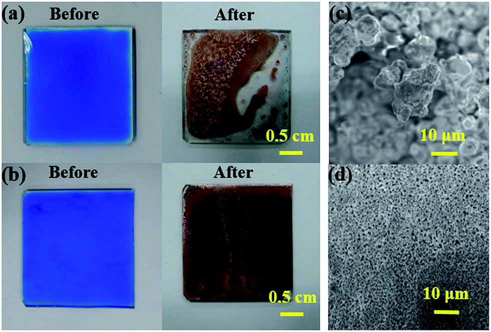 | ||
| Fig. 1 Copper thin film formation by heating (a) CuF–MIPA and (b) CuF–MIPA-OA ink on glass at 120 °C for 40 minutes. (c) and (d) show the SEM images of (a) and (b), respectively. In (a) and (b), both liquid films have the same total volume of 63 μL. | ||
The gas release generates bubbles, which can be large enough to create large holes in the heating process. Fig. 2 shows the time evolution of a heated CuF–MIPA thin film at 120 °C. Serious bubbling behavior is observed in the first few minutes, and results in serious liquid film deformation with several empty spots. The CuF–MIPA liquid film kept on dewetting in the evaporating/bubbling/copper formation process, as shown in Fig. 2. The SEM image (Fig. 1(c)) shows that the copper films are composed of porous and rough structures with large copper particles. These bubbles can also lead to more severe deformations for printed straight lines (Fig. S3†). The rough morphology caused by the gas release thus needs to be minimized to create continuous conductive patterns from the MOD ink.
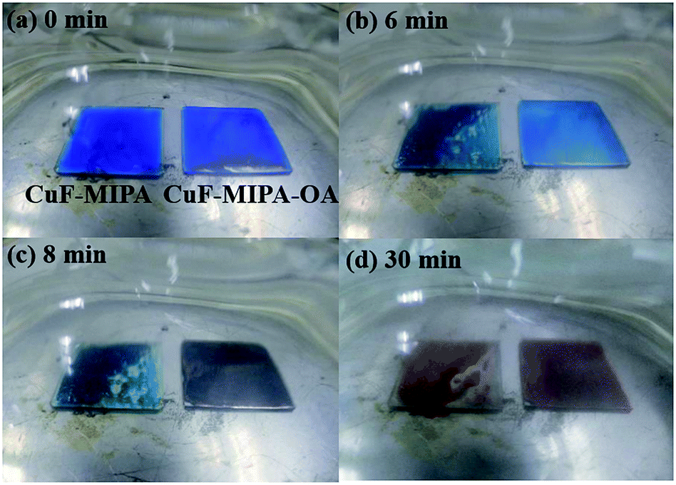 | ||
| Fig. 2 Time evolution of copper complex decomposition processes at 120 °C under nitrogen atmosphere. | ||
To enhance the film uniformity, octylamine is added to reduce the surface tension and reduce the dewetting problem because of its low surface tension as well as good size control ability in the copper formation process, which can be attributed to the long alkyl chain of octylamine.29,35 The addition of octylamine (OA) can effectively reduce the surface tension and contact angle of the MOD copper ink. As shown in Fig. 3(a), a minimum surface tension of ∼25 mN m−1 and contact angle of ∼22° are observed when an OA/MIPA ratio greater than 0.5 is used. The smaller surface tension leads to smaller bubble sizes,36 and reduce the perturbation of liquid films in the reaction step. The bubble sizes and numbers are calculated when copper starts to nucleate (Fig. S4†). The results show that bubble size and number is greatly reduced when OA/MIPA ratio is more than 0.5, which is consistent with the results of surface tension measurement. Moreover, the lower contact angle or better wettability inhibits contact line motion in the drying process. Thus, the resulting copper thin films show much better uniformity with an OA/MIPA ratio > 0.5 (Fig. 3(b)) as shown in Fig. 1(c) and (d) and 2, severe bubbling behavior is successfully mitigated and a compact and uniform copper thin film can be synthesized. Because the edges of CuF–MIPA liquid film on glass are slightly dewetted, the film might be thicker and leads to more bubbling rate compared with the thinner film of CuF–MIPA–OA ink. To confirm the relationship between the bubbling rate and liquid film thickness, two CuF–MIPA–OA films of different thickness are prepared and heated. It is found the bubble size and bubbling rates remain unchanged as the copper thin films started to form (Fig. S5†), indicating liquid film thickness does not affect bubbling behavior. With detail SEM image analyses (Fig. S6†), the particle size distributions at various OA/MIPA ratios are evaluated. The particle size obviously decreases when OA/MIPA ratio increases, and reaches a minimum at OA/MIPA = 1. Because OA has a higher boiling point (179.4 °C) than that of MIPA (160 °C), removal of OA content in the calcination process needs either a higher temperature or a longer drying time. Therefore, an optimum OA/MIPA ratio of 1.0 is used to formulate the CuF–MIPA–OA ink in the following sections to reduce both calcination temperature and drying time for the MOD copper ink.
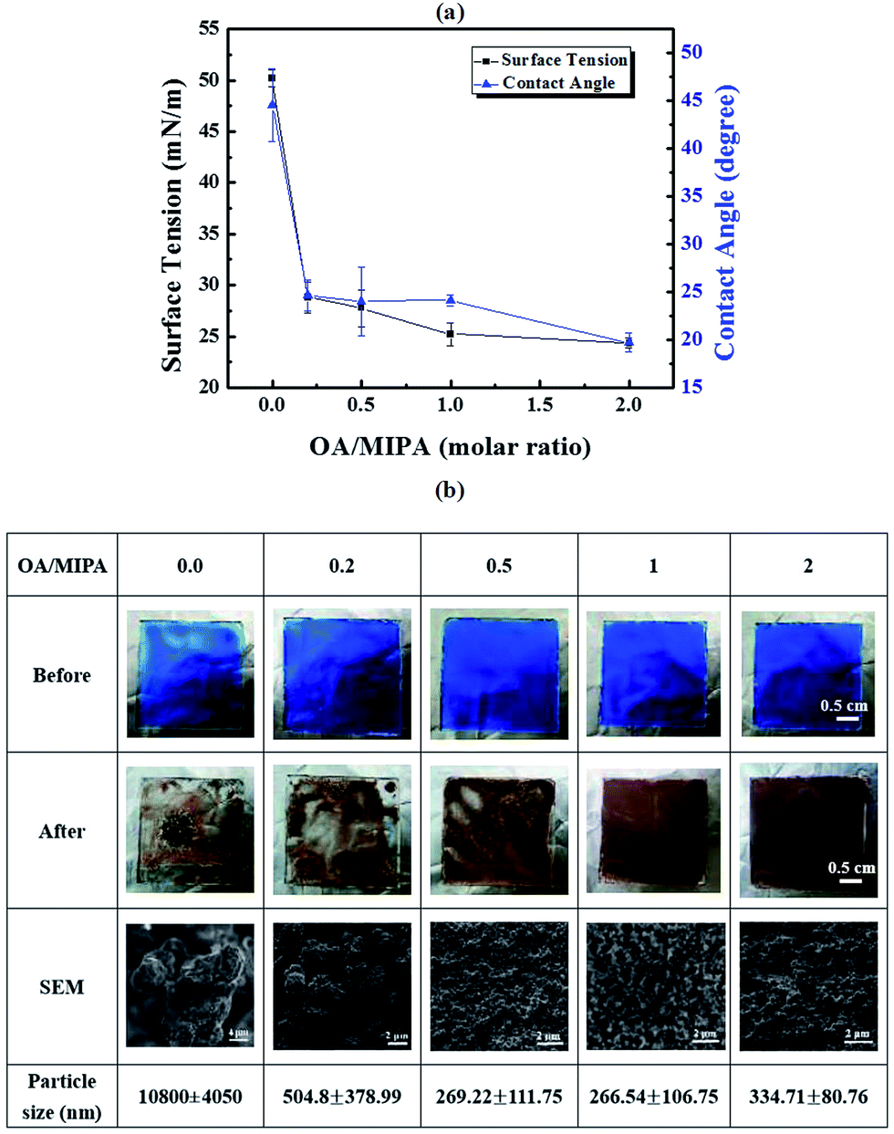 | ||
| Fig. 3 (a) Variation of surface tension and contact angle with the OA/MIPA ratio. (b) Surface morphology of copper complex thin films before and after calcination at 120 °C for 40 minutes. For all the samples, the total content of CuF is fixed at 0.063 mmol. Detail information about particle distributions can be found in Fig. S6.† | ||
The CuF–MIPA–OA ink can yield in conductive films after calcination. First, thermogravimetric differential thermal analysis (TGA) is used to examine the reaction of CuF decomposition with amine complexing agents. As shown in Fig. 4 (a), the decomposition reaction occurs at around 150 °C, which is close to other CuF/amine MOD inks in the literature (Table S1†).27,28 However, DTA analyses (Fig. 4(b)) show a single peak around 140 °C in the DTA curve of CuF–MIPA ink, but two major peaks in that of CuF–MIPA–OA ink, indicating that there might be two CuF complex ions in the CuF–MIPA–OA ink. The formation a new complex may lead to a different decomposition mechanism. To further investigate the effects of heating process on the electrical resistivity, inks with equal amount of CuF are spread on glass to form liquid films. The liquid films are subsequently calcined under nitrogen atmosphere at temperatures between 100–150 °C for 40 minutes. Fig. 5(a) shows the relationship between the resistivity and heating temperatures. After heating at 100 °C for 40 minutes, because of the high boiling point of IPA (160 °C) and OA (179.4 °C), the synthesized copper thin film still has unevaporated solvent residues or some unreacted copper complex ink, thus a fairly high resistivity is observed. For temperatures higher than 110 °C, the resistivity of the copper films decreases and is in the order of 10−7 Ω m. The SEM images indicate that the synthesized copper films show a compact network of nanoparticles (Fig. 5(b) and (c)). These particles have diameters ranging from 50 nm to 500 nm (Fig. S7†), which are much smaller than those from CuF–MIPA ink (>10 μm, Fig. 3(b)). The cross-sectional view (Fig. 5(c)) also shows a uniform and compact particle packing. The compact particle packing provides great percolating path for electron transfer and thus enhances the conductivity of the copper thin films.
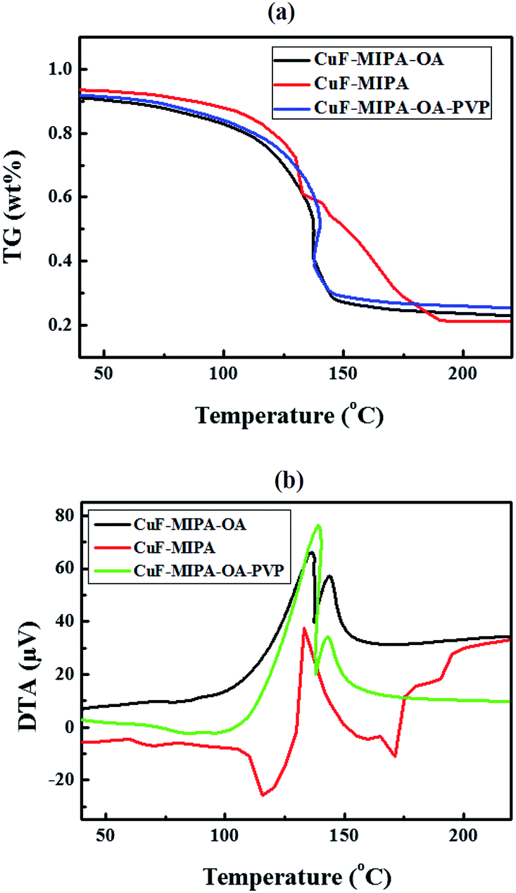 | ||
| Fig. 4 (a) TG and (b) DTA curves for the CuF–MIPA, CuF–MIPA–OA and CuF–MIPA–OA–PVP ink at a ramping rate of 5 °C min−1 under nitrogen flow of 100 cm3 min−1. | ||
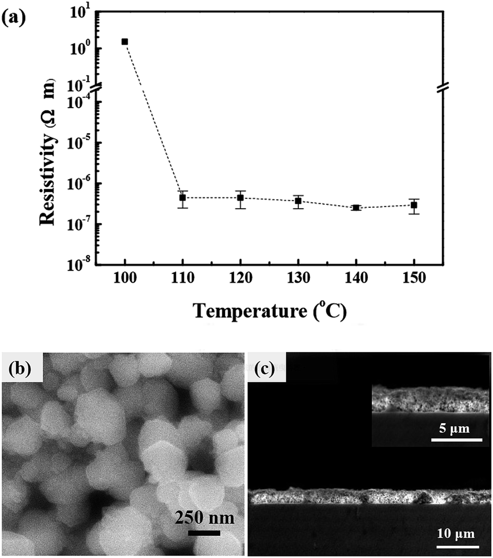 | ||
| Fig. 5 (a) Resistivity of copper thin film after calcination of CuF–MIPA–OA ink for 40 minutes as a function of sintering temperatures. (b) SEM image at 140 °C. (c) The cross section profile of (b). | ||
X-ray diffraction is also used to probe the crystalline structures in the copper thin films (Fig. S2(b)†). The peak assignments of XRD patterns at are in good agreement with the characteristic values for metallic copper crystalline structure. For inks heated at temperatures above 100 °C, the copper complex can be reduced to metallic copper with nearly no copper oxides after calcination. However, considering the time for solvent removal, a heating temperature higher than 110 °C might be more adequate to obtain conductive copper thin film within 40 minutes.
The resistivity of the copper films also depends on the calcination time (Fig. 6). As expected, both copper recovery reaction and solvent removal rates are slow at 110 °C. Therefore, it takes more than 40 minutes for the copper thin film to become conductive. The reaction and evaporation rates can both be accelerated by increasing the calcination temperature. As the temperature increases to 125 °C, it takes only 15 minutes to prepare the conductive copper thin films. When the temperature rises to 140 °C, the copper complex decomposition can be fast enough to prepare conductive copper thin films within 5 minutes.
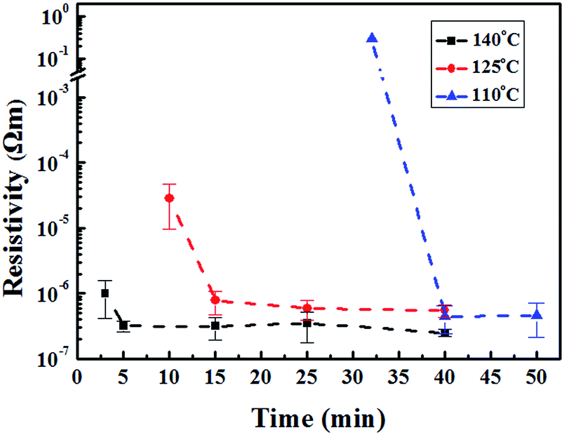 | ||
| Fig. 6 Variation of resistivity of copper thin films with calcination time at various calcination temperatures. | ||
Although copper conductive films can be fabricated successfully at low temperatures, they show poor adhesion to the substrates. Simple tape tests are performed to examine the adhesion of synthesized copper films on glass after PVP addition. A simple tape test is performed to test the adhesion of copper films on glass by removing the attached tape (Scotch Cat. 600 tape, 3M). As shown in Fig. 7(a), the copper films without PVP addition can be easily stripped off by tapes. To enhance the adhesion, PVP polymer is added into the CuF–MIPA–OA ink to serve as an adhesion promoter. PVP dissolves well in CuF–MIPA–OA ink and no precipitation or color change is observed (Fig. S1†). The addition of PVP in the CuF–MIPA–OA ink also shows the same thermal decomposition behavior as that of CuF–MIPA–OA ink (Fig. 4).
 | ||
| Fig. 7 A simple tape test for copper thin films produced from CuF–MIPA–OA ink (a) without PVP and (b) with 1 wt% PVP. (c) The sheet resistance increase ratio (R/R0) of sample (b) under repeated tape tests. (d) Resistivity as a function of copper thin films as a function of PVP content. All the copper thin films are obtained at a sintering temperature of 140 °C for 10 minutes under nitrogen environment. | ||
After the addition of PVP, the adhesion of the resulting copper thin films is greatly improved. As shown in Fig. 7(b), with the addition of 1 wt% PVP, copper films stay on the glass completely in the tape test, indicating great adhesion between the copper films and glass substrate. This great adhesion leads to the nearly unchanged sheet resistance after repeatedly taped for 10 times (Fig. 7(c)). However, the electrical conductivity might be deteriorated with PVP addition. The electrical resistance of the copper films with various PVP concentrations in CuF–MIPA–OA inks are measured and summarized in Fig. 7(d). The sheet resistance increases slightly when 1% PVP is added. As the content of PVP increases beyond 2 wt%, the sheet resistance increases sharply. When PVP concentrations is higher than 3 wt%, a high resistance in the order of 106 Ω sq−1 is observed, showing poor conductive networks of copper particles surrounded by PVP. Considering both the conductivity and adhesion, 1 wt% PVP is used in the following sections.
Conductive copper patterns can be plotted on flexible substrates with the same copper ink by using a microdispenser. As shown in Fig. 8(a), continuous copper thin lines of 250 μm in width are printed on a flexible polyimide thin film to test the mechanical stability. Fig. 8(c) shows the change in sample resistance after repeated bending. The resistance increase ratio (R/R0) rises only slightly (∼30%) after being bent repeatedly for more than 5000 bending cycles. This gradual loss of conductivity with bending cycle could attribute to the grain defects in the copper thin film patterns.24 The resulting copper thin films can serve as conductive tracks for lighting devices even under bending conditions (Fig. 8(b)). One can also create copper thin patterns on PET films with a lower calcination temperature and a longer sintering time. Fig. S8† shows the photograph of a copper pattern created on a PET thin film with a line width of 250 μm after sintering the ink pattern at 100 °C for 2 hours. These examples show that this copper MOD ink can be readily used for preparation of flexible conductors.
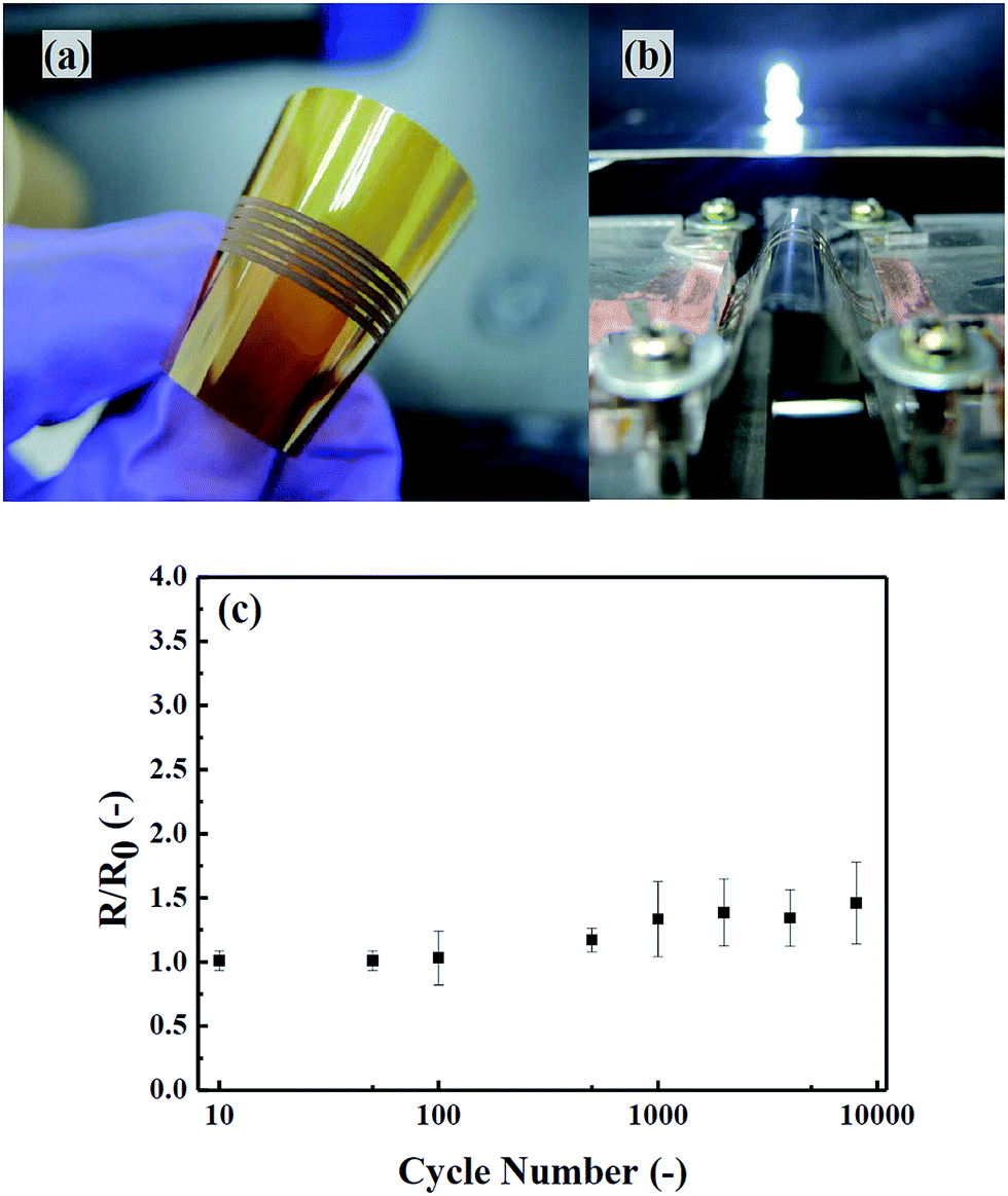 | ||
| Fig. 8 (a) Demonstration of the flexible copper thin film patterns produced from CuF–MIPA–OA ink. (b) Demonstration of printed copper thin film tracks on a bent PET sheet. The LED in the back is lighted by wiring the bent tracks to a power supply. (c) The sheet resistance increase ratio of sample (a) under repeated bending tests with a radius of curvature of 2 mm. | ||
Conclusions
A thermally triggered self-reducible copper ink is developed to print conductive patterns on flexible substrates. Inks containing only copper formate (CuF) and monoisopropanol amine (MIPA) generate large bubbles in the CuF decomposing process, and thus result in largely non-uniform copper thin films. With the addition of octylamine (OA), the bubbling disturbance is relieved due to better wettability and lower surface tension, so that the film uniformity is greatly improved. A low resistivity of 2 × 10⁻⁷ Ω m (8.5% of bulk copper) can be reached by heating the ink at 140 °C for 5 minutes under nitrogen environment. The results from XRD indicate the sintered copper films comprised of pure metallic copper crystalline. The adhesion of synthesized copper thin films on substrates can be greatly improved by addition of PVP without losing the conductivity, and the conductivity remains nearly the same after repeated tape tests. The ink can also be printed on flexible substrates, such as PET or PI thin films, to create highly-conductive tracks with great mechanical stability under bending conditions. Various conductive patterns on flexible substrates are also demonstrated to show the great potential of this ink for printed electronic applications. In summary, this ink formulation shows a fast synthetic route for copper patterns on flexible substrates and opens an avenue for potential applications in printed electronic devices.Acknowledgements
The authors are grateful to Hokkaido University and the Ministry of Science and Technology (MOST) of Taiwan for supporting this study. TY thanks Canon Foundation for partial financial support to this work. YCL and KMH thank Hokkaido University for the support to their stay in Sapporo.Notes and references
- S. Jeong, H. C. Song, W. W. Lee, S. S. Lee, Y. Choi, W. Son, E. D. Kim, C. H. Paik, S. H. Oh and B. H. Ryu, Langmuir, 2011, 27, 3144–3149 CrossRef CAS PubMed.
- Y. Lee, J. R. Choi, K. J. Lee, N. E. Stott and D. Kim, Nanotechnology, 2008, 19, 415604 CrossRef PubMed.
- S. Jang, Y. Seo, J. Choi, T. Kim, J. Cho, S. Kim and D. Kim, Scr. Mater., 2010, 62, 258–261 CrossRef CAS.
- J. S. Kang, H. S. Kim, J. Ryu, H. T. Hahn, S. Jang and J. W. Joung, J. Mater. Sci.: Mater. Electron., 2010, 21, 1213–1220 CrossRef CAS.
- K. Woo, Y. Kim, B. Lee, J. Kim and J. Moon, ACS Appl. Mater. Interfaces, 2011, 3, 2377–2382 CAS.
- D. Deng, Y. Jin, Y. Cheng, T. Qi and F. Xiao, ACS Appl. Mater. Interfaces, 2013, 5, 3839–3846 CAS.
- C.-J. Wu, Y.-J. Sheng and H.-K. Tsao, J. Mater. Chem. C, 2016, 4, 3274–3280 RSC.
- K. K. B. Hon, L. Li and I. M. Hutchings, CIRP Annals - Manufacturing Technology, 2008, 57, 601–620 CrossRef.
- B. K. Park, D. Kim, S. Jeong, J. Moon and J. S. Kim, Thin Solid Films, 2007, 515, 7706–7711 CrossRef CAS.
- A. Maattanen, P. Ihalainen, P. Pulkkinen, S. X. Wang, H. Tenhu and J. Peltonen, ACS Appl. Mater. Interfaces, 2012, 4, 955–964 Search PubMed.
- Y. L. Tai and Z. G. Yang, J. Mater. Chem., 2011, 21, 5938–5943 RSC.
- P. C. Hidber, W. Helbig, E. Kim and G. M. Whitesides, Langmuir, 1996, 12, 1375–1380 CrossRef CAS.
- T. B. Carmichael, S. J. Vella and A. Afzali, Langmuir, 2004, 20, 5593–5598 CrossRef CAS PubMed.
- F. Basarir, ACS Appl. Mater. Interfaces, 2012, 4, 1324–1329 CAS.
- C. C. Tseng, Y. H. Lin, Y. Y. Shu, C. J. Chen and M. D. Ger, J. Taiwan Inst. Chem. Eng., 2011, 42, 989–995 CrossRef CAS.
- D. Zabetakis and W. J. Dressick, ACS Appl. Mater. Interfaces, 2012, 4, 2358–2368 CAS.
- K. Cheng, M. H. Yang, W. W. W. Chiu, C. Y. Huang, J. Chang, T. F. Ying and Y. Yang, Macromol. Rapid Commun., 2005, 26, 247–264 CrossRef CAS.
- A. Sridhar, J. Reiding, H. Adelaar, F. Achterhoek, D. J. van Dijk and R. Akkerman, J. Micromech. Microeng., 2009, 19, 085020 CrossRef.
- Y.-C. Liao and Z.-K. Kao, ACS Appl. Mater. Interfaces, 2012, 4, 5109–5113 CAS.
- C.-Y. Kao and K.-S. Chou, Electrochem. Solid-State Lett., 2007, 10, D32–D34 CrossRef CAS.
- B. Lee, Y. Kim, S. Yang, I. Jeong and J. Moon, Curr. Appl. Phys., 2009, 9, E157–E160 CrossRef.
- D. P. Li, D. Sutton, A. Burgess, D. Graham and P. D. Calvert, J. Mater. Chem., 2009, 19, 3719–3724 RSC.
- Z. K. Kao, Y. H. Hung and Y. C. Liao, J. Mater. Chem., 2011, 21, 18799–18803 RSC.
- J. J. Valeton, K. Hermans, C. W. Bastiaansen, D. J. Broer, J. Perelaer, U. S. Schubert, G. P. Crawford and P. J. Smith, J. Mater. Chem., 2010, 20, 543–546 RSC.
- T. Araki, T. Sugahara, J. Jiu, S. Nagao, M. Nogi, H. Koga, H. Uchida, K. Shinozaki and K. Suganuma, Langmuir, 2013, 29, 11192–11197 CrossRef CAS PubMed.
- S. Cho, Z. Yin, Y.-k. Ahn, Y. Piao, J. Yoo and Y. S. Kim, J. Mater. Chem. C, 2016, 4, 10740–10746 RSC.
- A. Yabuki, N. Arriffin and M. Yanase, Thin Solid Films, 2011, 519, 6530–6533 CrossRef CAS.
- Y. Farraj, M. Grouchko and S. Magdassi, Chem. Commun., 2015, 51, 1587–1590 RSC.
- D.-H. Shin, S. Woo, H. Yem, M. Cha, S. Cho, M. Kang, S. Jeong, Y. Kim, K. Kang and Y. Piao, ACS Appl. Mater. Interfaces, 2014, 6, 3312–3319 CAS.
- A. Yabuki and S. Tanaka, Mater. Res. Bull., 2012, 47, 4107–4111 CrossRef CAS.
- Y.-H. Choi and S.-H. Hong, Langmuir, 2015, 31, 8101–8110 CrossRef CAS PubMed.
- C. Paquet, T. Lacelle, B. Deore, A. Kell, X. Liu, I. Korobkov and P. Malenfant, Chem. Commun., 2016, 52, 2605–2608 RSC.
- T. Yonezawa, H. Tsukamoto, Y. Yong, M. T. Nguyen and M. Matsubara, RSC Adv., 2016, 6, 12048–12052 RSC.
- W. Li, S. Cong, J. Jiu, S. Nagao and K. Suganuma, J. Mater. Chem. C, 2016, 4, 8802–8809 RSC.
- W. Xu and T. Wang, Langmuir, 2016, 33, 82–90 CrossRef PubMed.
- E. Brujan, Cavitation in Non-Newtonian Fluids: With Biomedical and Bioengineering Applications, Springer Science & Business Media, 2010 Search PubMed.
Footnote |
| † Electronic supplementary information (ESI) available. See DOI: 10.1039/c7ra01005b |
| This journal is © The Royal Society of Chemistry 2017 |