DOI:
10.1039/C7RA00922D
(Paper)
RSC Adv., 2017,
7, 18428-18437
Optical band gap tuning by laser induced Bi diffusion into As2Se3 film probed by spectroscopic techniques
Received
21st January 2017
, Accepted 15th March 2017
First published on 27th March 2017
Abstract
Amorphous chalcogenide semiconducting materials are very sensitive to electromagnetic radiation and are useful for infrared optics and play a pivotal role in modern technology. In the present article, As2Se3 and bilayer Bi/As2Se3 thin films were prepared by thermal evaporation method. The 532 nm laser induced diffusion of active Bi top layer into barrier As2Se3 film was probed through spectroscopic techniques. An X-ray diffraction study reveals no structural change due to laser irradiation while the optical parameters are affected by both Bi addition and laser irradiation which brings a change in the transmittivity and absorption coefficient. The indirect optical band gap is found to be decreased by 0.11 eV due to Bi addition to As2Se3 which is explained on the basis of density of defect states with an increase in disorder. The laser irradiated Bi diffusion increases the optical band gap by 0.05 eV (photobleaching) with a decrease in disorder. The Tauc parameter and Urbach energy which measures the degree of disorder change with Bi doping and irradiation. The refractive index is modified by the illumination process which is useful for optical applications. The optical property change is well supported by X-ray photoelectron core level spectra and Raman spectra.
1. Introduction
Metal chalcogenides are an important class of materials due to their extensive applications in various areas of science and technology and because of their unique properties such as high absorption coefficient, intrinsic large dipole moment, convenient band gap tailoring, large capacity for multiple excitations, and solution processability. These properties make them suitable for promising light sensitizers for high-efficiency quantum dots, extremely thin absorbers and counter electrodes in sensitized solar cells.1,2 The high transmission power in the infrared region of these materials shows potential applications in infrared photonics, infrared waveguides, optical fibers, thermoelectrics, photosensitizers, superconductors and ultrafast-laser inscribed chalcogenide glass waveguide and active and passive IR devices.3–8 The presence of lone pairs of electrons in chalcogen atoms influences the optical and electrical properties.9,10 Photo-induced effects are very predominant in chalcogenide materials due to the presence of localized states in the gap that leads to very rich behavior under the influence of light.11 The internal and surface structures along with the optical absorption (red or blue shift) of chalcogenides are modified by the illumination process.12 The photo interaction in chalcogenide films with photo-doping or photo-dissolution of metals into the chalcogenide matrix is useful for various device-making applications.13–15
Due to its short lifetime and low sensitivity, pure Se is not a useful candidate for device application.16,17 This limitation is overcome with addition of some impurity atoms like As, Bi, Te, Sb etc., making the new alloy useful with higher sensitivity, crystallization and smaller aging effects.18 The addition of an impurity has a pronounced effect on the optical properties and this effect is widely different for different impurities.19–21 The increased metallic property and larger polarizability of Bi brings a carrier type reversal from p- to n-type with the addition of a critical quantity of Bi in the amorphous Ge–Se system.22 The incorporation of Bi into As2Se3 leads to a considerable change in its structural and optical properties.23,24 However, the method of impurity addition plays a significant role in fundamental research in the field of disordered materials.
Photo-induced diffusion is one of the interesting ways for impurity addition to a host matrix that modifies the optical constants. The present article reports the optical and structural changes resulting from the deposition and diffusion of Bi into an As2Se3 matrix. The laser intensity drives the Bi layer into the As2Se3 film which facilities the formation of Bi–As–Se solid solution that brings about changes in optical properties such as transmittance, absorption, refractive index, and optical band gap. These optical property changes are investigated using various spectroscopic techniques. The change in optical parameters was calculated from the optical transmission obtained from Fourier transform infrared (FTIR) spectra. X-ray photoelectron spectroscopy (XPS) measurements show the photo-induced bonding change in the bilayer film. Direct evidence of the optical changes is seen from Raman spectra.
2. Experimental
The bulk sample of As2Se3 was prepared by the melt-quenching technique by taking As and Se (99.999% pure, Sigma-Aldrich). The chemicals were weighed according to their atomic percentage and were sealed in a quartz ampoule in a vacuum of ∼10−5 Torr. The sealed ampoule was kept inside a rotating furnace at 950 °C for 24 h to make the melt homogeneous. The bulk sample was obtained by quenching the ampoule in ice-cooled water. Thin films of As2Se3 and Bi/As2Se3 were prepared by the thermal evaporation technique inside a coating system (HIND-HIVAC Model 12A4D) from the prepared bulk As2Se3 and Bi (99.999% pure Sigma-Aldrich) at a base pressure of 1 × 10⁻⁶ Torr onto glass substrates. The bilayer film is made by the co-evaporation method without breaking the vacuum as the coating unit consists of two separate boats. We kept both the samples (As2Se3 and Bi) on two boats inside the vacuum chamber before creating the vacuum. When the required vacuum condition is reached, we first deposited the As2Se3 film of 800 nm that is measured from a thickness monitor attached to the coating system. During the deposition of the bottom As2Se3 layer, the shutter of the Bi-containing boat was closed. After the first layer (As2Se3) deposition, the As2Se3 boat shutter was closed automatically and the Bi boat shutter opened and a Bi layer of 7 nm was deposited onto the As2Se3 layer. So, there is no breaking of the vacuum during the deposition of the bilayer film, and there is no chance of air exposure of the As2Se3 layer before Bi deposition so that no O2 layer was deposited onto it. The thickness is initially set up in the programme, such that after reaching the required thickness, the deposition automatically stops. The thickness reading is seen from the thickness display monitor of a quartz crystal thickness monitor. The thicknesses of the As2Se3 and Bi/As2Se3 films were 800 nm and 807 nm (800 nm bottom As2Se3 layer and 7 nm top Bi layer) respectively. In order to get homogeneous films, mechanical rotation of the substrate holder was carried out during the deposition process. The temperature rise of the substrate due to resistive heating from the boat was negligible.
The elemental composition and presence of elements in the prepared films were checked by energy dispersive X-ray analysis (EDAX) with a Sirion XL 40 to which SEM is attached. The scan was done at 20 kV with 40 μA emission current exposing a sample of 1 cm2 size at 2 × 10⁻⁷ Torr pressure. The estimated average precision was less than 5% in atomic fraction for each element (Table 1). The amorphous state of the film was checked by X-ray diffraction (XRD; Philips, CuKα, λ = 1.54 Å). We irradiated the bilayer Bi/As2Se3 film at room temperature by a diode pumped solid state laser of wavelength 532 nm with a power of 40 mW in order to diffuse the Bi into the As2Se3 matrix by photo-diffusion. The film was mounted on a sample holder and the laser light was focused into a 2 mm wide spot. The increase in temperature at the illuminated region was calculated according to a procedure described elsewhere25 and was estimated to be 8 K. This small increment in temperature is not enough to induce any of the observed phenomena due to local heat. Hence, the observed changes are not due to thermal effects but mainly due to photo-induced effects.26,27 The optical transmission data of the As2Se3 and as-prepared, irradiated Bi/As2Se3 films were recorded with a FTIR spectrometer (Bruker Optics IFS66v/S) in the visible wavelength range of 500–900 nm. The measurement was done inside the sample chamber of the spectrometer in dark condition. The reflection loss was not that much as compared to the high absorption in the band gap region.
Table 1 The measured elemental composition from EDAX for As2Se3 thin film
| Element |
Calculated weight% |
Observed weight% |
Calculated atomic% |
Observed atomic% |
| Se |
61.26 |
60.42 |
60 |
58.46 |
| As |
38.74 |
39.58 |
40 |
41.54 |
| Totals |
100.00 |
100.00 |
100.00 |
100.00 |
The surface analytic technique of XPS will give valuable information about the new bonds formed between the components due to photo-diffusion of Bi into the As2Se3 matrix. The XPS measurements were first made on the As2Se3 and as-prepared Bi/As2Se3 films and then for the Bi-diffused Bi/As2Se3 illuminated film. The XPS core level and valence band spectra were obtained with monochromatic Al Kα X-rays (1486.6 eV) at a vacuum of 1.33 × 10⁻⁷ Pa using a Multilab 2000 Thermo Scientific UK instrument. The XPS data consisted of survey scans over the entire binding energy (BE) and selected scans over the core level peaks of interest. An energy increment of 1 eV was used for recording the survey spectra and 0.05 eV for the case of core level spectra. The core level peaks were recorded by sweeping the retarding field and using a constant pass energy of 30 eV. Data were averaged by taking three scans. The reproducibility of the measurements was checked on different portions of the investigated surfaces. For this study, adventitious carbon was used as a reference and the BE of the reference C 1s line was set as 284.6 eV.28,29 To eliminate the charging effect, for each sample, a calibration factor was calculated from the difference between the measured C 1s BE and the reference value of 284.6 eV.30 The original BE data were corrected according to the calibration factor. Raman spectroscopic measurements were obtained with a Raman spectrometer (LabRAM HR system) using a 514.5 nm argon laser with a CCD detector in backscattering geometry in a range of 50–500 cm−1. The spectral resolution of the spectrometer was 0.5 cm−1. All data were recorded using 2 mW of laser power, which was not sufficient to induce any crystallization in the sample. The intensity of the laser light near the sample was very low and the data acquisition time was within 50 s.
3. Results and discussion
3.1. EDAX analysis
The EDAX analysis carried out on the as-prepared As2Se3 film suggests that the compositions are very close to those of the starting materials (Table 1). The variation in calculated and observed values is within 5%. Fig. 1 and 2 show the presence of Se, As and Bi in the as-deposited As2Se3 film and Bi/As2Se3 film.
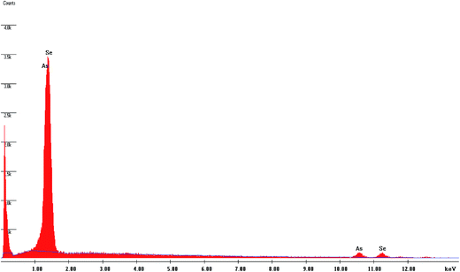 |
| | Fig. 1 EDAX spectrum of as-prepared As2Se3 thin film. | |
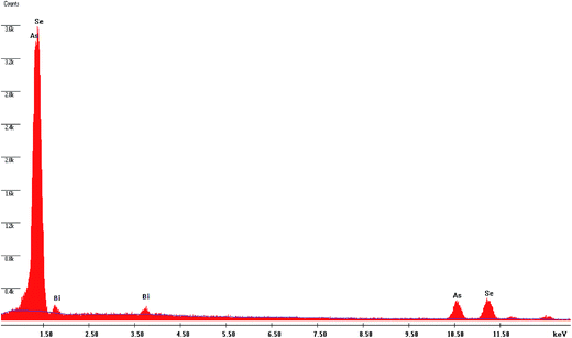 |
| | Fig. 2 EDAX spectrum of Bi/As2Se3 thin film. | |
3.2. XRD analysis
The XRD spectra for the three thin films are shown in Fig. 3. The absence of sharp structural peaks for all three thin films confirms the amorphous nature of the samples. The XRD spectra are very similar to each other, so that we cannot determine any differences between the films. The width of the broad hump was from 15° to 40°. The result shows that there was no structural change as a result of Bi diffusion into the As2Se3 layer due to laser irradiation.
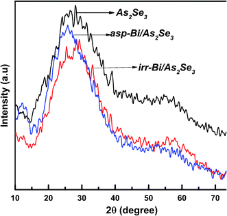 |
| | Fig. 3 XRD patterns of As2Se3, and as-prepared and irradiated Bi/As2Se3 bilayer thin films. | |
3.3. FTIR analysis
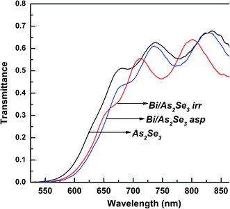
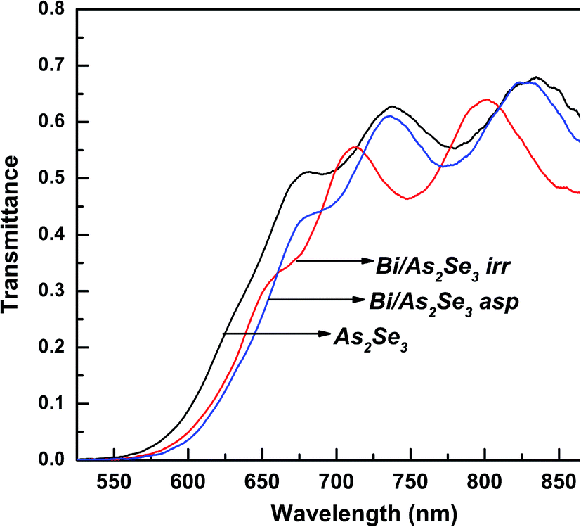
The transmission spectra for the three films (As2Se3, as-prepared Bi/As2Se3 and irradiated Bi/As2Se3) are presented in Fig. 4. The interference fringes observed in these spectra beyond 650 nm wavelength of the incident beam refer to the transmission range of the films. These interference fringes indicate the homogeneity and smoothness of the deposited films. The refractive index of the films is calculated from the transmission range. The transmittance is decreased from 70% (As2Se3) to 68% (asp-Bi/As2Se3) when Bi is deposited onto As2Se3. It further reduced to 65% (irr-Bi/As2Se3) due to laser induced diffusion of Bi into As2Se3.
 |
| | Fig. 4 Transmission spectra of As2Se3, and as-prepared and irradiated Bi/As2Se3 bilayer thin films. | |
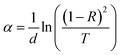
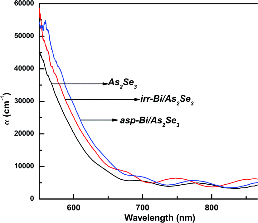
Absorption coefficient and optical band gap measurement. The strong absorption region lies in the wavelength range of 550–650 nm as seen from Fig. 4. The optical constants like absorption coefficient and optical bandgap are calculated from this region. The absorption coefficient (α) is calculated from the transmission data by using the equation| |
 | (1) |
where d is the thickness of the film measured by thickness monitor, T is the transmission and R as the reflection of the films. The d value for As2Se3 film is 800 nm and is 807 nm for the Bi/As2Se3 bilayer film. The reflection loss was not that much as compared to the high absorption in the band gap region. The fundamental edge in crystalline materials is directly related to the transitions from the conduction band to valence band that are associated with direct and indirect band gaps. Due to the absence of an electronic band structure in k-space in the case of amorphous materials, the transitions are termed as non-direct. A photon of known energy excites an electron from a lower to a higher energy state that corresponds to an absorption edge. The absorption coefficient decreases with wavelength, which can be seen from Fig. 5. The decrease in α with wavelength implies that the material is becoming transparent at higher wavelength, which makes it a useful optical material. The α value is found to be increased for Bi/As2Se3 film compared with As2Se3 and it decreased for the laser-induced Bi-diffused Bi/As2Se3 bilayer film which is also seen in other studies.31,32 The increment in α is a consequence of structural and surface defects caused by light exposure.33,34 The absorption edge in amorphous materials which follows an exponential nature is divided into three types, namely residual below-gap absorption, Urbach tails and inter-band absorption.35
 |
| | Fig. 5 α vs. λ plots for As2Se3, and as-prepared and irradiated Bi/As2Se3 bilayer thin films. | |
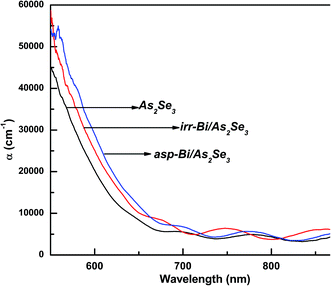
The optical absorption spectrum is the most productive tool for developing an energy band diagram. The optical band gap (Eg) was calculated from the absorption data by using the non-direct transition model in the case of amorphous semiconductors,36 proposed by Tauc.37 The effective optical band gap in the high absorption region (α > 104 cm−1) is determined by using the following equation:
| | |
(αhν)1/2 = B1/2(hν − Eg)
| (2) |
where
α,
h,
ν,
Eg and
B are the absorption coefficient, Planck's constant, frequency, optical band gap, and a constant (Tauc parameter) respectively.
38 Plotting the linear portions of the dependence of (
αhν)
1/2 on photon energy (
hν) will give a straight line, with the
y intercept giving the value of the optical band gap as shown in
Fig. 6. The optical band gap
Eg of As
2Se
3 (1.76 ± 0.01 eV) is reduced to 1.65 ± 0.01 eV when Bi is deposited onto As
2Se
3. This decrease in band gap by 0.11 eV is explained on the basis of density of defect states with an increase in disorder. The optical absorption in amorphous materials depends on short-range order and defects associated with it. The decrease in optical band gap can be explained on the basis of the “density of state model” proposed by Mott and Davis.
39 The model proposes that the width of the localized states near the mobility edges depends on the degree of disorder and defects present in the amorphous structure. The presence of high concentration of localized states in the band structure is responsible for the decrease of optical band gap. This reduction in the band gap may also be due to the shift in Fermi level, whose position is determined by the distribution of electrons over the localized states.
40
 |
| | Fig. 6 (αhν)1/2 vs. (hν) plots for As2Se3, and as-prepared and irradiated Bi/As2Se3 bilayer thin films. | |
Absorption is generally due to a transition from the top of the valence band to the bottom of the conduction band as seen in the fundamental absorption region. The deposition of Bi layer onto As2Se3 thin film may cause an increase in the density of states in the valence band structure as the Bi layer modifies the surface structure at the interface. This can be noticed from the Tauc parameter (slope of the absorption coefficient B1/2) decreasing from 781 cm−1/2 eV−1/2 (As2Se3) to 691 cm−1/2 eV−1/2 (Bi/As2Se3) due to an increase in disordering. The Tauc parameter carries information regarding the compactness of the valence and conduction band states. This also includes the nature of optical transitions which reflects the k selection rule along with the disorder-induced spatial correlation of optical transitions.38 This is a very useful parameter to determine the degree of disorder which is very sensitive to topological disorder only when electronic structural changes occur as observed by Zanatta and Chambouleyron.38 The electronic structural changes might be occurring in the bilayer surface due to the Bi layer as a result of which B1/2 is decreased. The reduction of Eg can be explained by the increased tailing of the band tails in the gap.41
On the other hand, the irradiated bilayer film showed a photo-bleaching phenomenon (increase in band gap due to illumination) due to the diffusion of the top Bi layer into the bottom As2Se3 layer. The optical change is clearly seen from the different optical parameters obtained for the illuminated film as compared to the asp-Bi/As2Se3 bilayer film. The reduction of transmission, increase in absorption coefficient and increase of the band gap of 0.05 eV from the as-prepared bilayer film are due to the diffusion of Bi into the As2Se3 matrix. The Bi layer has diffused into the As2Se3 layer for a certain distance which depends on the diffusion length of Bi and has formed a three-component solid solution of Bi–As–Se in the diffused region. This type of solid solution formation has been studied in other different types of films42–44 and is responsible for the increase in optical band gap of the irradiated film. After inter-diffusion, the three-component Bi–As–Se solid solution is created with the decreasing width of the optical band gap in comparison with homogeneous amorphous As2Se3 film. The diffusion creates more heteropolar bonds which are responsible for the increase in the band gap that we have seen in the XPS core level spectra which will be discussed in the next section. The increase in B1/2 for the irradiated film (735 cm−1/2 eV−1/2) was due to the decrease in disorder (increase of heteropolar bonds)32 that increases the width of the gap between the valence and conduction bands, thus increasing the optical band gap. A decrease in the density of such localized states may enlarge the band gap leading to the blue shift of the electronic absorption edge.45 The disorder in the as-prepared film is mainly due to the wrong Bi–Bi, Se–Se or As–As homopolar bonds and As (Se) dangling bonds.46 Therefore, the intrinsic structural change in the photo-bleaching process has been proposed due to the increase in the Bi–Se, As–Se bond density and the subsequent increase in structural ordering. The intrinsic structural changes are ascribed to the following photoreaction
| |
 | (3) |
The illumination process creates local structural ordering in the Bi/As2Se3 bilayer thin films with homopolar bonds (Bi–Bi, Se–Se or As–As) being converted into (Bi–Se, As–Se) heteropolar bonds. This observation is in agreement with the fact that the latter bonds are stronger than the former bonds and are more favored as the glass tries to reach the thermal equilibrium of the lowest free energy.47 The increase in structural ordering due to minimum number of homopolar bonds causes an increase in optical band gap since the state of band tails in the glasses is mainly induced by the homopolar bonds.48
In the low absorption region (α < 104 cm−1), the absorption coefficient α shows an exponential dependence on photon energy hν, and obeys the Urbach relation49
| |
α(hν) = α0![[thin space (1/6-em)]](https://www.rsc.org/images/entities/char_2009.gif) exp(hν/Ee) exp(hν/Ee)
| (4) |
where
α0 is a constant and
Ee corresponds to the Urbach energy (the width of the band tail of the localized states in the band gap). Plotting the dependence of log(
α) on photon energy will give a straight line and the inverse of the slope gives the width of the tails of the localized states in the gap at band edges known as the Urbach edge (
Ee). The Urbach energy is a useful parameter to evaluate the degree of disorder. The Urbach energy for As
2Se
3 film is found to be 159 meV which becomes 273 meV for the as-prepared Bi/As
2Se
3 film. This increase in Urbach energy clearly shows the increase of disorders due to Bi deposition onto As
2Se
3 film. The lower values of Urbach energy
Ee of the irradiated Bi/As
2Se
3 film (198 meV) over the as-prepared Bi/As
2Se
3 film (273 meV) imply that the illuminated film is more structurally ordered than the as-prepared film, which may be due to the creation of heteropolar bonds after the photo-diffusion of Bi into the As
2Se
3 matrix. Note that the Urbach energy and Tauc parameters vary inversely though both represent the degree of disorder. This local microstructural ordering can predominantly influence the film density which in turn can lead to a decrease in the refractive index for the irradiated film.
11
Refractive index calculation. The refractive index is modified by the diffusion process which is useful for optical applications. According to Swanepoel,50 in the transparent region where the absorption coefficient α ≈ 0, the refractive index (n) is given by
| n = [N + (N2 − S2)1/2]1/2 |
where 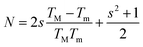 in which TM and Tm are the corresponding transmission maxima and minimum at a certain wavelength λ and s is the refractive index for glass substrate (1.51).
The refractive index of the as-prepared Bi/As2Se3 bilayer film is found to be increased compared with the As2Se3 film and again it is decreased due to Bi diffusion into the As2Se3 film as shown in Fig. 7. Generally speaking, a decrease/increase in the band gap (red shift/blue shift in the absorption edge) is accompanied by an increase/decrease in the refractive index according to Moss's rule (Egn4 ∼ constant).51,52 The thermally induced diffusion of Bi into As2Se3 film in the Bi/As2Se3 bilayer film can be achieved by a thermal annealing process. The thermal diffusion will change the optical as well as the structural properties as discussed in other papers.53,54
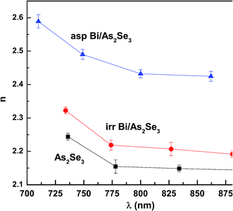 |
| | Fig. 7 Refractive index of As2Se3, and as-prepared and irradiated Bi/As2Se3 bilayer thin films. | |
3.4. XPS analysis
We have used the surface analytic XPS technique to investigate the different bonds present and newly created due to Bi deposition and laser induced diffusion into the As2Se3 layer. The atomic movements due to Bi diffusion into As2Se3 layer are probed through XPS.
Typical XPS spectra of As2Se3 and Bi/As2Se3 film contain many photoelectron peaks and Auger peaks of Se, Bi and As. But, we have considered only the core peaks such as Se 3d, As 3d, Bi 4f and Bi 5f for the present study. The XPS spectrum shows no Bi peak for the As2Se3 film while Bi 5d peak appears in the spectra of Bi/As2Se3 bilayer films (as-prepared and irradiated) as shown in Fig. 8. The As2Se3 core level peak was at 43.16 eV which reflects the presence of AsSe3 and As–AsSe2 bonds. But, the spectral intensity as well as BE changed with more peaks after Bi deposition onto As2Se3 layer. The As 3d peak position for as-prepared Bi/As2Se3 bilayer film was located at 42.75 eV with a decrease of 0.41 eV in BE that implies the formation of more As–As homopolar bonds. The As 3d peak for the irradiated film is found to be decreased and the peak is broadened and found to be shifted from the as-prepared one to 42.86 eV. This indicates a decrease in As–As homopolar bonds and formation of As–Se heteropolar bonds. Because As (2.18) has a smaller electronegativity than Se (2.55), homopolar As–As bond-containing units contribute the lower BE peak.55
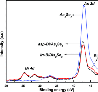 |
| | Fig. 8 XPS core level spectra of Bi 4d and As 3d of As2Se3, and as-prepared and irradiated Bi/As2Se3 bilayer thin films. | |
The Bi atom bonded to two Se atoms shows doublets at higher BE, while Bi atom bonded to one Se and one Bi atom shows also doublets at lower BE. This is because Bi (2.02) has smaller electronegativity than Se (2.55).55 More Bi2O3 formation takes place due to the exposure of the film to atmosphere during irradiation, whereas it is less for the as-prepared one due to high-vacuum condition (Fig. 8).
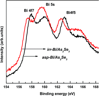
The Se 3d core level spectrum for the As2Se3 film contains no Bi peak, whereas Bi 4f and Bi 5s peaks appear in the spectrum of the as-prepared Bi/As2Se3 bilayer film due to Bi deposition onto As2Se3 film (Fig. 9). The binding energy of Bi 4f7/2 peak for as-prepared Bi/As2Se3 bilayer film is at 157.93 eV which shifts to 157.37 eV after Bi diffusion into the As2Se3 layer. The Bi 4f5/2 peak which was at 163.11 eV for as-prepared Bi/As2Se3 bilayer film shifts to lower BE (162.58 eV) after Bi diffusion. This shift of BE towards lower energy for the Bi 4f peak indicates the creation of more Bi–Se heteropolar bonds after photo-diffusion. The Bi 5s peak intensity for the irradiated film (159.56 eV) is found to be increased compared with that for the as-prepared film which appeared at 160.06 eV, supporting the formation of more heteropolar bonds.
 |
| | Fig. 9 XPS core level spectra of Bi 4f and Bi 5s of as-prepared and irradiated Bi/As2Se3 bilayer thin films. | |
The intensity of Se 3d peak of Bi/As2Se3 is decreased when Bi is deposited onto the As2Se3 layer. The BE of the Se 3d peak for As2Se3 which was at 55.10 eV also shifted to 55.17 eV for the as-prepared Bi/As2Se3 bilayer film. This BE shift towards higher energy indicates the formation of more homopolar bonds. The laser induced diffusion of Bi into As2Se3 changes the position of Se 3d to 54.91 eV as shown in Fig. 10. This shifting in BE towards lower energy is due to the large number of Bi–Se bonds that are formed. This is because Se has higher electronegativity than As and Bi. So, more heteropolar bonds are formed due to irradiation which decreases the disorder resulting in an increase in optical band gap.
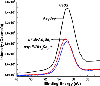 |
| | Fig. 10 XPS core level spectra of Se 3d of As2Se3, and as-prepared and irradiated Bi/As2Se3 bilayer thin films. | |
3.5. Raman analysis
Raman spectroscopy is an effective method for studying the structure of non-crystalline materials. The analysis of the vibrational spectra of these substances yields useful information about the chemical bonding type and atomic arrangement order. Direct evidence of structural changes in As2Se3 thin films caused by Bi deposition and diffusion was obtained from Raman spectra.
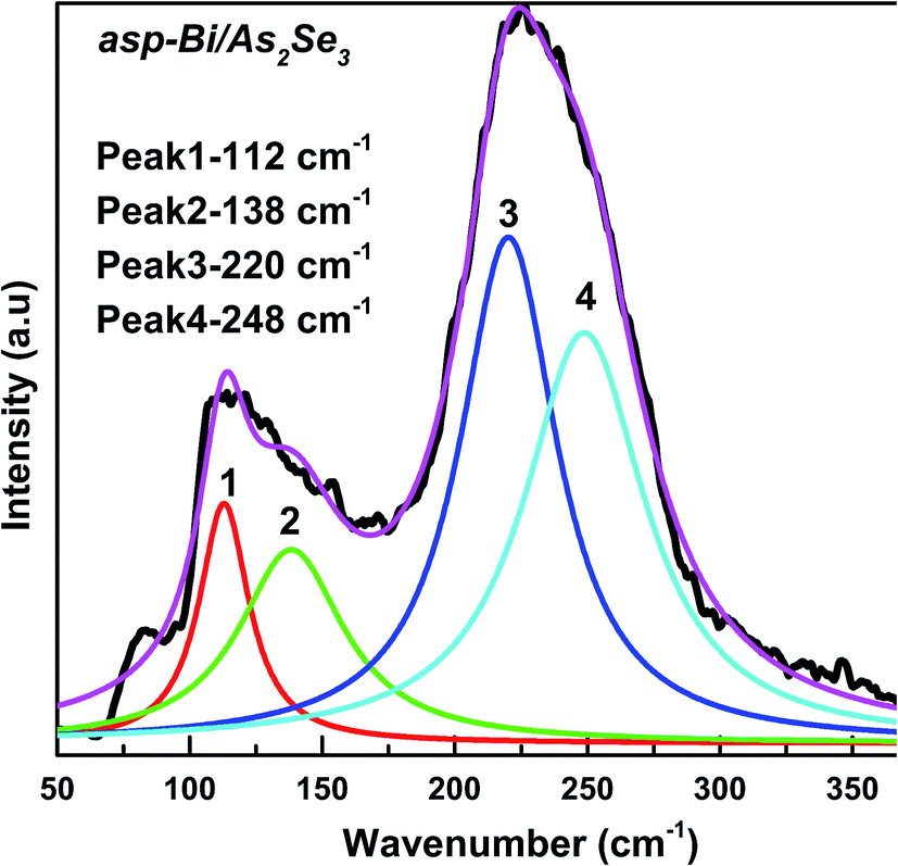
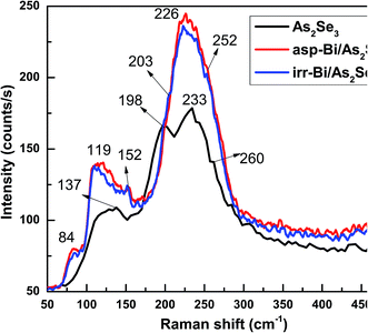
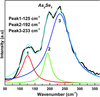
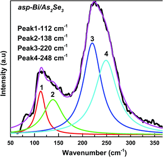
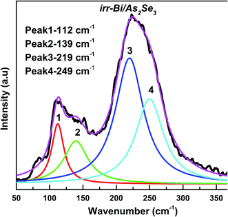
The Raman spectrum of As2Se3 contains peaks at 137, 198, 233, and 260 cm−1 as seen in Fig. 11. The As–As homopolar bonds are represented by the peaks at 137 and 198 cm−1 while the main band at 233 cm−1 is due to the As–Se vibration in As–Se–As.56 The band at 260 cm−1 corresponds to the Se–Se bond vibration57 (Fig. 11). The deconvoluted As2Se3 Raman spectrum only shows three peaks at 125, 192 and 233 cm−1 (Fig. 12) which are nearly the same as the peaks identified in Fig. 11. The peaks at 125 and 192 cm−1 correspond to As–As homopolar bonds, for which the area under the curve is shown in Table 2. With deposition of Bi onto As2Se3, the new compound Bi/As2Se3 has peaks at 84, 119, 152, 226, and 252 cm−1 (Fig. 11). The new band at 84 cm−1 can be attributed to asymmetric stretching modes of the Bi–Bi chain in the amorphous matrix.58 The peak at 137 cm−1 for As2Se3 shifts to 119 cm−1 due to Bi deposition and lower still (109 cm−1) due to diffusion of Bi into As2Se3. With deconvolution, as-prepared Bi/As2Se3 has a peak at 138 cm−1 that corresponds to the As–As homopolar bonds with an increase in area under the peak compared to the As2Se3 film (125 cm−1) as shown in Fig. 13. At the same time the deconvoluted peak at 220 cm−1 corresponds to the As–Se vibrational units the strength of which decreases (area under the curve) from 233 cm−1 of As2Se3 as seen from Table 2. The change in intensity at this peak clearly shows the density of bonds. The peak at 248 cm−1 (Fig. 13) refers to the Se–Se homopolar bonds whose area under the curve is found to be more than the area under the curve for irradiated Bi/As2Se3 film (Fig. 14). This decrease in area for the irradiated film confirms the decrease of Se–Se homopolar bonds that reduces the disorder. This decrease may indicate that irradiation also increases ordering in the local structures.59,60 The additional peak at 203 cm−1 for the irradiated Bi/As2Se3 film (Fig. 11) shows the presence of Bi–Se vibrational mode which is close to the value reported in ref. 61. The area under the peak at 219 cm−1 in the deconvoluted spectrum (Fig. 14) is increased compared with the corresponding peak in Fig. 13, confirming the increase in the density of heteropolar As–Se bonds. The new peak at 152 cm−1 also shows the appearance of Bi–Se whose intensity is more for the irradiated film implying the formation of more heteropolar bonds due to laser induced diffusion (Fig. 11). The main band at 233 cm−1 shifts to lower wavenumber of 220 cm−1 after Bi deposition onto As2Se3 and shows the change in chemical disorder. The decrease in area under the peak at 112 cm−1 in the deconvoluted spectra for as-prepared compared with irradiated Bi/As2Se3 bilayer thin film that refers to the Bi–Bi bonds shows the decrease in disorder. The peak shift can be easily noticed in the two spectra which clearly supports the optical changes in the film. The analysis of Raman spectra of both films suggests that the film structure is modified through conversion of a pair of homopolar bonds to heteropolar bonds decreasing the structural disorder. However, there is no change in the structure (amorphous) as seen from the XRD result. The formation of the coordinative metal–chalcogen bonds (Bi–Se) does not lead to the destruction of the structural units of the glass, and can influence only the dynamical characteristics of the structural elements. Under the formation of such bonds during the photo-doping process, the ions of metal are diffused along the sites of the lone-pair electrons belonging to the chalcogen atoms. The formation of the normal metal–chalcogen covalent bonds occurs by means of metal diffusion on the sites of defects of the amorphous matrix.62
 |
| | Fig. 11 Raman spectra of As2Se3, and as-prepared and irradiated Bi/As2Se3 bilayer thin films. | |
 |
| | Fig. 12 Deconvoluted Raman spectrum of As2Se3 thin film. | |
Table 2 Peak positions and corresponding areas under the curve of As2Se3, and as-prepared and irradiated Bi/As2Se3 bilayer thin films
| Sample |
Peak 1 |
Peak 2 |
Peak 3 |
Peak 4 |
| As2Se3 |
Peak position |
125 |
192 |
233 |
|
| Area |
2903 |
2162 |
14324 |
|
| Asp-Bi/As2Se3 |
Peak position |
112 |
138 |
220 |
248 |
| Area |
2123 |
3511 |
8484 |
8535 |
| Irr-Bi/As2Se3 |
Peak position |
112 |
139 |
219 |
249 |
| Area |
2036 |
2962 |
10191 |
6800 |
 |
| | Fig. 13 Deconvoluted Raman spectrum of as-prepared Bi/As2Se3 thin film. | |
 |
| | Fig. 14 Deconvoluted Raman spectrum of irradiated Bi/As2Se3 thin film. | |
4. Conclusion
The optical changes in the Bi/As2Se3 bilayer film are due to the formation of solid solution of Bi–As–Se after the photo-induced diffusion of Bi into the As2Se3 matrix. The intermixing process creates Bi–Se and As–Se units that indicates that diffusion is the dominant reason for photo-optical transformation by laser irradiation. The indirect optical band gap is found to be decreased which is due to Bi addition onto As2Se3 that is explained on the basis of density of defect states with an increase in disorder. The laser irradiation enhances Bi diffusion which increases the optical band gap (photo-bleaching) with a decrease in disorder. The refractive index is modified by the irradiation process which is useful for optical applications. The X-ray photoelectron spectroscopy measurements show the different bonding behavior due to photo-induced diffusion. The irreversible nature of the optical properties for this material can be used for archival memory, creation of optical mirrors, and integrated optical elements, which need high local changes of optical parameters. By selecting suitable pairs of chalcogenide glasses with different optical gaps, one can modify the parameters of the light-sensitive layers and use them for optical recording.
References
- Z. Pan, I. Mora-Sero, Q. Shen, H. Zhang, Y. Li, K. Zhao, J. Wang, X. Zhong and J. Bisquert, J. Am. Chem. Soc., 2014, 136(25), 9203–9210 CrossRef CAS PubMed.
- Y. Tanabe, K. K. Huynh, R. Nouchi, S. Heguri, G. Mu, J. Xu, H. Shimotani and K. Tanigaki, J. Phys. Chem. C, 2014, 118(7), 3533–3538 CAS.
- P. Ma, D.-Y. Choi, Y. Yu, X. Gai, Z. Yang, S. Debbarma, S. Madden and B. Luther-Davies, Opt. Express, 2013, 21, 29927–29937 CrossRef PubMed.
- P. Toupin, L. Brilland, J. Trolès and J. L. Adam, Opt. Mater. Express, 2012, 2(10), 1359 CrossRef CAS.
- K. Onar and M. E. Yakinci, J. Alloys Compd., 2015, 620, 210 CrossRef CAS.
- W.-J. Tzeng, M.-L. Wu, Li-J. Lin and H.-Y. Chang, J. Alloys Compd., 2015, 651, 483 CrossRef CAS.
- G. Sun, X. Qin, D. Li, J. Zhang, B. Ren, T. Zou, H. Xin, S. B. Paschen and X. Yan, J. Alloys Compd., 2015, 639, 9 CrossRef CAS.
- P. Sharma, M. Vashistha, V. Ganesan and I. P. Jain, J. Alloys Compd., 2008, 462, 452 CrossRef CAS.
- P. Sharma, M. S. El-Bana, S. S. Fouad and V. Sharma, J. Alloys Compd., 2016, 667, 204 CrossRef CAS.
- R. Naik, R. Ganesan and K. S. Sangunni, J. Alloys Compd., 2013, 554, 293 CrossRef CAS.
- R. Naik, S. Jena, R. Ganesan and N. K. Sahoo, Laser Phys., 2015, 25, 036001 CrossRef.
- J. P. DeNeufville, S. C. Moss and S. R. Ovshinsky, J. Non-Cryst. Solids, 1974, 13, 191 CrossRef CAS.
- A. V. Kolobov and S. R. Elliott, Adv. Phys., 1991, 40, 625 CrossRef CAS.
- T. Wagner, E. Márquez, J. Fernández-Pena, J. M. González-Leal, P. J. S. Ewen and S. O. Kasap, Philos. Mag. B, 1999, 79, 223 CrossRef CAS.
- M. Behera and R. Naik, Appl. Phys. A, 2016, 122, 913 CrossRef.
- A. A. Al-Ghamdi, Vacuum, 2006, 80, 400 CrossRef CAS.
- M. Saitar, J. Ledru, A. Hamou and G. Saffarini, Phys. B, 1998, 245, 256 CrossRef.
- R. Golovchak, H. Jain, O. Shpotyuk, A. Kozdras, A. Saiter and J.-M. Saiter, Phys. Rev. B: Condens. Matter Mater. Phys., 2008, 78, 014202 CrossRef.
- P. Chen, P. Boolchand and D. G. Georgiev, J. Phys.: Condens. Matter, 2010, 22, 6 Search PubMed.
- R. Naik, P. P. Sahoo, C. Sripan and R. Ganesan, Opt. Mater., 2016, 62, 211 CrossRef CAS.
- N. E. Mott, Philos. Mag., 1969, 19, 835 CrossRef CAS.
- S. Sharma, P. Kumar and R. Thangaraj, Curr. Appl. Phys., 2013, 13, 731 CrossRef.
- M. M. El-Nahass, A. F. El-Deeb, H. E. A. El-Sayed and A. M. Hassanien, Opt. Laser Technol., 2006, 38(3), 146 CrossRef CAS.
- K. A. Aly, A. A. Othman and A. M. Abousehly, J. Alloys Compd., 2009, 467, 417 CrossRef CAS.
- A. Ganjoo, K. Shimakawa, H. Kamiya, E. A. Davis and J. Singh, Phys. Rev. B: Condens. Matter Mater. Phys., 2000, 62, R14601 CrossRef CAS.
- A. Ganjoo and H. Jain, Phys. Rev. B: Condens. Matter Mater. Phys., 2006, 74, 024201 CrossRef.
- R. Naik, S. Jena, R. Ganesan and N. K. Sahoo, Phys. Status Solidi B, 2014, 251(3), 661 CrossRef CAS.
- J. F. Moulder, W. F. Sticker, P. E. Sobol and K. D. Bomben, Hand Book of X-ray Photoelectron Spectroscopy, Perkin Elmer, Eden Pairie, MN, 1992 Search PubMed.
- W. J. Stec, W. E. Morgan, R. G. Albridge and J. R. Van Wazer, Inorg. Chem., 1972, 11, 219 CrossRef CAS.
- T. L. Barr and S. Seal, J. Vac. Sci. Technol., A, 1995, 13, 1239 CAS.
- A. M. Andriesh and M. S. Iiovu, J. Optoelectron. Adv. Mater., 2006, 8, 2080 CAS.
- R. Naik, C. Kumar, R. Ganesan and K. S. Sangunni, Mater. Chem. Phys., 2011, 130(1), 750 CrossRef CAS.
- A. V. Kolobov, Photoinduced Metastability in Amorphous Semiconductors, Wiley-VCH, Weinheim, 2003 Search PubMed.
- R. Chauhan, A. K. Srivastava and A. Tripathy, Prog. Nat. Sci.: Mater. Int., 2010, 20, 54 CrossRef.
- R. Naik, S. K. Parida, C. Kumar, R. Ganesan and K. S. Sangunni, J. Alloys Compd., 2012, 522, 172 CrossRef CAS.
- E. Marquez, J. M. Gonz alez-Leal, A. M. Bernal-Oliva, T. Wagner and R. Jimenez Garay, J. Phys. D: Appl. Phys., 2007, 40, 5351 CrossRef CAS.
- J. Tauc, Amorphous and Liquid Semiconductors, Plenum Press, NewYork, NY, USA, 1979 Search PubMed.
- A. R. Zanatta and I. Chambouleyron, Phys. Rev. B: Condens. Matter Mater. Phys., 1996, 53, 03833 CrossRef CAS.
- N. F. Mott and E. A. Davis, Electronics Processes in Non-Crystalline Materials, Clarendon, Oxford, 1979. p. 428 Search PubMed.
- T. T. Nang, M. Okuda, T. Matsushita, S. Yokota and A. Suzuki, Jpn. J. Appl. Phys., 1976, 14, 849 CrossRef.
- P. Nagels, L. Tichy, A. Triska and H. Ticha, J. Non-Cryst. Solids, 1983, 59–60, 1015 CrossRef CAS.
- R. Naik, R. Ganesan and K. S. Sangunni, J. Alloys Compd., 2010, 505, 249 CrossRef CAS.
- V. Takats, P. Nemec, A. Csik and S. Kokenyesi, J. Phys. Chem. Solids, 2007, 68, 948 CrossRef CAS.
- R. Naik, R. Ganesan, K. V. Adarsh, K. S. Sangunni, V. Takats and S. Kokenyesi, J. Non-Cryst. Solids, 2009, 355, 1939 CrossRef CAS.
- T. T. Nang, M. Okuda and T. Matsushita, Phys. Rev. B: Condens. Matter Mater. Phys., 1979, 19, 947 CrossRef.
- T. Kawaguchi and S. Maruno, J. Appl. Phys., 1993, 73, 4560 CrossRef CAS.
- Q. Yan, H. Jain, J. Ren, D. Zhao and G. Chen, J. Phys. Chem. C, 2011, 115, 21390 CAS.
- W.-H. Wei, S. Xiang, S.-W. Xu, L. Fang and R. P. Wang, J. Appl. Phys., 2014, 115, 183506 CrossRef.
- F. Urbach, Phys. Rev., 1953, 92, 1324 CrossRef CAS.
- R. Swanepoel, J. Phys. E: Sci. Instrum., 1983, 16, 1214 CrossRef CAS.
- P. Knotek and L. Tichy, Mater. Res. Bull., 2012, 47, 4246 CrossRef CAS.
- R. Naik, C. Sripan and R. Ganesan, Opt. Laser Technol., 2017, 90, 158 CrossRef CAS.
- P. Nemec, J. Jedelsky, M. Frumar, M. Stabl and M. Vlcek, J. Phys. Chem. Solids, 2004, 65, 1253 CrossRef CAS.
- R. Naik, R. Ganesan and K. S. Sangunni, Mater. Chem. Phys., 2011, 125, 505 CrossRef CAS.
- W. Li, S. Seal, C. Rivero, C. Lopez, K. Richardson, A. Pope, A. Schulte, S. Myneni, H. Jain, K. Antoine and A. C. Miller, J. Appl. Phys., 2015, 98, 053503 CrossRef.
- V. Kovanda, M. Vlček and H. Jain, J. Non-Cryst. Solids, 2003, 326 & 327, 88 Search PubMed.
- Z. G. Ivanova, V. Pamukchieva and M. Vleck, J. Non-Cryst. Solids, 2001, 293–295, 580 CrossRef CAS.
- L. Kumari, J.-H. Lin and Y.-R. Ma, J. Phys. D: Appl. Phys., 2008, 41, 025405 CrossRef.
- P. K. Dwivedi, S. K. Tripathi, A. Pradhan, V. N. Kulkarni and S. C. Agarwal, J. Non-Cryst. Solids, 2000, 266–269, 924 CrossRef CAS.
- E. Sleeck, L. Tichy, P. Nagels and R. Callaerts, J. Non-Cryst. Solids, 1996, 198–200, 723 CrossRef.
- X. Liu, D. J. Smith, J. Fan, Y.-H. Zhang, H. Cao, Y. P. Chen, J. Leiner, B. J. Kirby, M. Dobrowolska and J. K. Furdyna, Appl. Phys. Lett., 2011, 99, 171903 CrossRef.
- A. V. Stronski, M. Vlcek, A. I. Stetsun, A. Sklenar and P. E. Shepeliavyi, Semicond. Phys., Quantum Electron. Optoelectron., 1999, 2(2), 63 Search PubMed.
|
| This journal is © The Royal Society of Chemistry 2017 |
Click here to see how this site uses Cookies. View our privacy policy here. 
 Open Access Article
 This Open Access Article is licensed under a Creative Commons Attribution-Non Commercial 3.0 Unported Licence
 *
*


 in which TM and Tm are the corresponding transmission maxima and minimum at a certain wavelength λ and s is the refractive index for glass substrate (1.51).