
 Open Access Article
 This Open Access Article is licensed under a
 Creative Commons Attribution 3.0 Unported Licence
Ultra-high aspect ratio functional nanoporous silicon via nucleated catalysts†
Jatin J. Patil a,
Brendan D. Smithb and
Jeffrey C. Grossman*b
a,
Brendan D. Smithb and
Jeffrey C. Grossman*b
aDepartment of Chemical Engineering, University of Waterloo, ON, Canada N2L 3G1
bDepartment of Materials Science and Engineering, Massachusetts Institute of Technology, Cambridge, Massachusetts, USA 02139. E-mail: jcg@mit.edu
First published on 14th February 2017
Abstract
Nanoporous silicon (NPSi) has drawn recent interest because of its potential in a range of applications such as battery anodes, photocatalysis, thermoelectrics, and filtration membranes. However, the inexpensive and scalable manufacturing of high aspect ratio porous structures on the nanometer scale has been difficult due to the reliance of current methods on complex and expensive equipment used for techniques such as anodization or photolithography. Here, we report a method of producing NPSi with sub-10 nm pore sizes and aspect ratios as high as 400![[thin space (1/6-em)]](https://www.rsc.org/images/entities/char_2009.gif) :1 by leveraging the nucleation of sputtered noble metals on the Si surface, followed by metal-assisted chemical etching (MACE). The technique is capable of producing NPSi in an intrinsically scalable manner. Samples are characterized with SEM and TEM, along with vertical and horizontal FIB cross-sectional milling to elucidate the porous structure at several μm of depth within the substrate. Following preparation of the NPSi, it is functionalized with Al2O3 and TiO2 via atomic layer deposition (ALD). TiO2-functionalized NPSi exhibits reflectivity of 6–8% for visible wavelengths, and 2–3% in the infrared – showing its promise as a robust and functional porous substrate. The developed approach of employing MACE with sputtered nucleated catalysts facilitates the scalable fabrication of functional ultra-high aspect-ratio nanopores in silicon.
:1 by leveraging the nucleation of sputtered noble metals on the Si surface, followed by metal-assisted chemical etching (MACE). The technique is capable of producing NPSi in an intrinsically scalable manner. Samples are characterized with SEM and TEM, along with vertical and horizontal FIB cross-sectional milling to elucidate the porous structure at several μm of depth within the substrate. Following preparation of the NPSi, it is functionalized with Al2O3 and TiO2 via atomic layer deposition (ALD). TiO2-functionalized NPSi exhibits reflectivity of 6–8% for visible wavelengths, and 2–3% in the infrared – showing its promise as a robust and functional porous substrate. The developed approach of employing MACE with sputtered nucleated catalysts facilitates the scalable fabrication of functional ultra-high aspect-ratio nanopores in silicon.
Introduction
Nanoporous silicon (NPSi) has been a material of interest for decades, owing to its diverse range of potential applications. Since the first report on the material by Uhlir1 in 1956 NPSi fabrication techniques have demonstrated continuous advancement with regard to their ability to produce smaller pore sizes and higher pore aspect ratios. NPSi with precise pore morphology control shows promise as a versatile material due to its demonstrated potential application in optoelectronics,2 sensors,3,4 biological applications,5 flexible electronics6 and photovoltaics,7–11 where thin NPSi membranes are attractive for applications in nanofiltration12,13 and thermoelectrics.14–17Despite this potential, current methods of fabricating NPSi with large-area, monodisperse pore coverage are limited. Deep reactive ion etching and other dry etching techniques, commonly used for micro- and nanopore fabrication, are not well-suited for mass production.18 In addition, the highest aspect ratios reported with these techniques is approximately 125:1 for 35 nm wide trenches.19 In general, photolithography20 and electron-beam lithography21 have limited capabilities to generate sub-10 nm pores over a large area. Therefore, especially for larger scale applications such as catalysis or filtration, a simple and scalable strategy is needed.
Metal-assisted chemical etching (MACE) has been widely explored as a method to efficiently etch silicon to produce complex extruded 3D structures such as X-ray diffraction gratings22 with high precision on the sub-micron scale. The technique was utilized by Chang et al. in combination with block-copolymer lithography to form regular arrays of nanowires with aspect ratios of up to 220:1,23 as well as extensively in other work to show controllable extrusion of nanowires and nanostructures in silicon.24–27
The MACE process begins with deposition of noble-metal catalysts28 on the silicon surface, followed by introduction to an acidic oxidizing solution of hydrofluoric acid (HF) and hydrogen peroxide (H2O2). The reduction of H2O2 is catalyzed by the noble metal, which in turn locally injects holes (h+) into the silicon.29–32 This oxidizes the silicon, locally producing SiO2, which is subsequently dissolved by the HF present in the solution. The reaction scheme results in the continuous etching of the noble metal along preferred crystalline orientations, creating positive features that very closely match the shape of the patterned catalyst.33
NPSi can be generated via MACE by depositing noble metal nanoparticles on silicon to act as catalysts,34 where the etching rate is primarily limited by the diffusion of reactants and products to and from the noble metal at the pore bottom.35 However, using nanoparticles for etching has its own drawbacks – particle faceting results in different surface areas, where surface area is proportional to etch rate and direction.36 The etching directionality of MACE is dependent on h+ injection at the catalyst–silicon interface.37 Therefore, particles are prone to etch in unwanted directions if their largest facet is not perpendicular to the desired etch direction. Our recent work has demonstrated pore aspect ratios of over 100:1 using MACE with silica-coated gold nanoparticles, achieving sub-10 nm pore sizes with consistent, directional etching and a narrow size distribution over many square micrometers of substrate.38 However, this requires a relatively complex synthesis procedure, and would require uniform particles along with a sensitive monolayer deposition technique.
We demonstrate here a scalable method for the deposition of sub-5 nm noble metal nanoislands on the surface of Si, which subsequently yield ultra-high aspect ratio nanopores via the MACE process. The technique employs the DC magnetron sputtering of nominal gold and silver thin films (sub-1 nm thickness) under standard deposition conditions, which nucleate as Volmer–Weber island structures due to their low surface energies. These island structures have been studied extensively to elucidate film formation mechanics in magnetron sputtering.39,40 The method has been previously employed by Chung et al., where the film formation process is halted prior to full film coverage to investigate the plasmonic absorbance of Ag nanoislands pre- and post-annealing.41 In this work, we utilize a similar approach for the scalable deposition of sub-5 nm islands with 5–15 nm inter-particle spacing (refer to ESI† for nano-island spacing histograms). The use of magnetron sputtering also facilitates the deposition of island structures with planar catalyst–Si interfaces, which allows for more directional hole injection and subsequently a highly anisotropic etch. The approach developed here results in a fast, scalable method of producing nanoporous silicon with sub-10 nm pore size, extremely directional etching and aspect ratios as high as 400:1.
In addition to the capability of fabricating sub-10 nm ultrahigh aspect ratio pores in Si, the possibility of creating functional porous substrates via the conformal deposition of catalytic materials is explored here through the atomic layer deposition (ALD) of titanium dioxide (TiO2) – a popular photocatalyst that has been investigated extensively as a substrate for self-cleaning surfaces, water treatment, and hydrogen production.42–44 The ability of ALD to deposit conformal layers with sub-nanometer resolution45 can be further leveraged for the fabrication of a wide array of functional devices.44,46,47
Experimental
(100) silicon wafers (B-doped, thickness: 275 ± 25 μm, resistivity: 0.001–0.01 Ω cm) were solvent cleaned using a standard acetone–IPA–DI water rinse. Dried wafers were sputtered with AJA ATC 2200 UHV Sputter Coater under pre-deposition pressure of 5–10 × 10−8 Pa, Ar flow of 40 sccm, and deposition pressure of 4 mTorr. Targets were DC magnetron sputtered at 125 W. Deposition rates were 3.2 Å s−1 for Au and 4.0 Å s−1 for Ag. Following deposition, substrates were placed into the MACE solution (5.33 M HF, 0.12 M H2O2). Reaction was terminated by washing with water and removal of substrates, followed by drying with a N2 gun.Atomic layer deposition on porous samples
NPSi samples are coated using the Harvard CNS Benchtop ALD system. Al2O3 is coated via a static-flow process at 200 °C. Precursors are trimethylaluminum and H2O, with calculated growth rate of 1.14 Å per cycle. TiO2 is coated via static process at 190 °C. Precursors are tetrakis(dimethylamido)titanium and H2O with calculated growth rate of 0.45 Å per cycle.TEM cross section sample preparation
Planar view lamellae were prepared at a depth of 4 μm below the surface, extracted, and mounted to standard copper TEM grids using a FEI Helios 660 Focused Ion Beam instrument equipped with an Omniprobe.Characterization
Zeiss Ultra Plus Field Emission SEM, FEI Helios 660 Focused Ion Beam (FIB) with SEM (and attached EDAX Energy Dispersive X-ray Spectroscopy [EDS] Detector), JEOL 2100 Transmission Electron Microscope, and Thermo Scientific K-Alpha+ XPS are used. Image statistics are analyzed using ImageJ and MATLAB.Results and discussion
Deposition of nucleated noble metal islands for MACE is demonstrated here to be a promising strategy to produce porous silicon with sub-10 nm pore sizes. This method is both high-throughput and scalable, and demonstrates the versatility of the MACE technique to catalyze pore formation in a novel size-regime. While nanoparticles have previously been proposed as a solution to obtaining monodisperse pore size and spacing, they can exhibit inconsistency in their deposition and etching directionality.48 In addition, achieving highly ordered arrays of homogeneously spaced catalysts over large areas necessitates the use of ligands and very monodisperse particles, and requires precise control over chemistry and monolayer formation.49 The developed method of sputtering MACE catalysts removes this dependency on parameter-sensitive wet chemical processes and brings a simplified and established method of metal deposition, resulting in a simple two-step MACE synthesis process. The established approach is demonstrated in this work to be effective for the production of NPSi exhibiting morphological nanoscale homogeneity over many square centimeters, with no intrinsic limitations on the further scaling of the technique.The process of sputtering nominally thin-films of metal causes the nucleation of homogeneously spaced and sized islands.50 The size and morphology of islands is influenced by surface defects on the substrate51 and the interfacial energies of the metals with Si,52 where the metal surface energies (γ) are γAg = 1.246–1.250 J m−2, and γAu = 1.500–1.506 J m−2.53 Due to their wetting behavior on the native oxide surface, Au and Ag films nucleate as isolated islands instead of a continuous film. SEM and TEM images of nucleated islands resulting from sputtering 3 Å of Au and Ag are shown in Fig. 1, along with corresponding histograms of island size. Observed diameters of nucleated islands are 4.4 ± 0.9 nm for Ag (images in Fig. 1a–c) and 2.0 ± 0.9 nm for Au (Fig. 1d–f). The SEM images demonstrate the large-area coverage of the Au and Ag islands over the silicon substrate. This island formation is homogeneous over the entire sputtered and etched region of the silicon wafer. TEM images show the Volmer–Weber film nuclei. The advantages to this method over using conventional nanoparticle deposition or in situ nanoparticle growth are superior substrate–metal interface contact area, smaller particle size, narrower particle size distribution, and uniform catalyst spacing over large areas.
 | ||
| Fig. 1 Images of sputtered nucleated Ag taken with (a) SEM, (b) TEM. (c) Particle size histogram for Ag catalysts generated from the TEM image. Images of sputtered nucleated Au taken with (d) SEM, (e) TEM. (f) Particle size histogram for Ag catalysts generated from the TEM image. Target film thickness is 3 Å for both metals. | ||
Following sputter deposition, the wafer is placed in the MACE etchant solution. Etching of silicon is enabled by localized silicon oxidation, facilitated via catalytic reduction of H2O2 on noble metal nanoparticles. This is followed by etching of SiO2 by HF, allowing the metal nanoislands to continue etching normal to the Si surface. After etching, the nanopores of the NPSi are filled with Al2O3 via ALD to enhance imaging contrast and to preserve the porous morphology prior to characterization.
Characterization of pore sizes via image analysis, especially after Au-catalyzed MACE, is difficult due to the texturing of the Si surface during etching, a phenomenon possibly initiated by the formation and etching of Au-silicides in near proximity to the substrate surface. Diffusion of Au into Si has been noted at room temperature for Si treated with HF.54 This has the potential to cause Au-silicide formation and further unwanted etching of the surface. Similar effects have been reported with Ag catalysts, with particular reference to the formation of a mesoporous Si layer around etching sites.55 Though the aforementioned surface degradation makes direct pore size measurement difficult, the size of the metal catalysts fabricated for MACE should closely match the etched feature sizes, as shown in previous work evaluating the quality and precision of MACE.56
A further degree of control over nanoisland size could be employed via silicon surface treatment prior to catalyst nucleation. Removal of native oxide with HF prior to noble metal deposition increases wettability of the films. This in turn is expected to cause a lower metal island contact angle, but also higher likelihood of silicide formation.
The effect of contact angle on etching characteristics can be elucidated by comparing the etching behavior of Au and Ag metal islands, which exhibit different wetting behavior. With its lower surface energy, Ag has a higher contact angle with Si than does Au, thus forming more pronounced nanoislands, as seen in SEM (Fig. 1a and d). This, in turn, leads to more lateral etching on the surface prior to etching in the 〈100〉 direction – which is observed as linear tracks surrounding pores in Ag (Fig. 2c) when compared to Au, which has a lower contact angle (Fig. 2b).
 | ||
| Fig. 2 (a) Macroscopic view of (left to right) bare Si, Si etched with Au, Si etched with Ag, and a 25-cent coin for scale. SEM images of porous Si surfaces etched with (b) Au and (c) Ag SEM images of focused ion beam (FIB) milled cross-sections of (d) Au and (e) Ag etched NPSi (1 h etch time). Pores are back-filled with Al2O3 via ALD prior to FIB milling. (f) Reflectance spectra of NPSi coated with TiO2 via ALD post-etching (lines labelled with metal catalyst used). Reflectance data from 820–860 nm is omitted due to light-source switching. Inset shows reflectance data, including spectrum for bare Si (blue line). | ||
To verify the presence of nanopores and examine the morphology within the bulk of the sample following etching, TEM images of horizontal cross-sections of NPSi and a control Si sample prepared via FIB at a depth of 4 μm are compared. The resulting images demonstrate the presence of pores at depths beyond 4 μm into the substrate for the sample etched with sputtered Au, as visible in Fig. 3b. The ability to extract a 100 nm lamella at a 4 μm depth while maintaining the porous morphology also demonstrates the structural stability of the porous structure. In addition to the deposition of Al2O3, ALD is utilized here for the conformal coating of the NPSi pore walls with TiO2. This process yields a porous, high surface-area functional substrate, while its porosity results in anti-reflective properties. Nanostructured TiO2 has been explored for applications owing to its anti-reflective and self-cleaning properties.57–59 Fig. 2f shows reflectivity measurement TiO2-functionalized NPSi, demonstrating reflectance values between 2% and 8% over the UV-visible and short-IR wavelengths for both Au- and Ag-etched Si. While not achieving reflectances as low as those demonstrated for MACE-processed NPSi by Branz et al., which possessed 1–5% reflectance in the visible range,60,61 the NPSi produced here demonstrates promise due to its smaller pore size, and higher aspect-ratio. With these metrics, higher pore densities can be achieved, which correlate to higher functional surface area. Thus, we demonstrate NPSi functionalized with a deposited nanometer-thick layer of TiO2, with the potential of being a material with competitive light absorption and conversion properties.
 | ||
| Fig. 3 TEM images of planar lamellae of Si prepared via FIB at a 4 μm depth. (a) Schematic of lamellae preparation showing (1) removal of lamella from NPSi via Omniprobe and (2) TEM viewing perspective. (b) Native Si not exposed to the MACE process, and (c) Si with sputtered gold catalyst immersed in MACE solution for 1 hour. The darker contrast area on top-right corner of both images is the platinum protective layer deposited prior to planar sectioning. | ||
Coating of nanoscale, ultra-high aspect ratio pores of over 1000:1 has previously been demonstrated for anodized aluminum oxide (AAO).62 An SEM image of a FIB milled cross-section (Fig. 4a) and associated EDS analysis (Fig. 4b) confirms conformal TiO2 deposition into high aspect ratio pores to depths of roughly 1 μm below the substrate surface. Ti and O are both present above the dotted line (700 nm, EDS point 1) (Fig. 4b). The pores shown in Fig. 4a are fully filled with TiO2 for characterization, but can also be partially filled to maintain the nanoporous structure of the substrate. EDS point 2, at 1300 nm, shows no Ti presence. C and Ga are present due to the substrate and surface contamination and ion implantation, respectively. The lack of a Ti signal indicates the absence of the porous regime. The coated NPSi surface was characterized via XPS to confirm the composition of the ALD coating. High resolution element scans confirm the stoichiometry of the TiO2 coating: deconvolution of the O 1s peak into TiO2 (ref. 63) and SiO2 (ref. 64) yields a O:Ti ratio of 2.3:1 (see ESI† for XPS data and analysis). These results demonstrate the realization of NPSi with sub-10 nm, ultra-high aspect ratio pores, which can be made functional via the ALD deposition of TiO2.
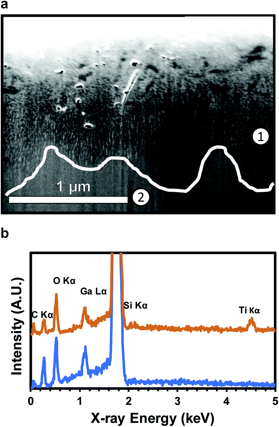 | ||
| Fig. 4 (a) FIB cross section of NPSi etched with Au islands and coated with TiO2. TiO2-filled pore area is lighter in contrast to silicon background. The white line illustrates lowest visible pore depth along cross-section. (b) EDS analysis of the SEM region shown: scan at 700 nm (spot 1) shows the presence of TiO2, while a scan at 1300 nm (spot 2) from surface lacks TiO2 (A and B). The Si peak is cut off due to a strong signal from the underlying substrate. | ||
Conclusions
In this work, a MACE process which utilizes sputtered nucleated noble metal nanoislands as catalysts for etching has been introduced. By leveraging interfacial effects and the nature of film formation, sub-5 nm noble metal islands are nucleated on silicon uniformly over multiple square centimeters. The developed technique is advantageous when compared to other MACE schemes such as nanoparticle deposition and patterned features due to the islands' narrow size distribution and planar interface with the Si, reducing the occurrence of unwanted etching effects resulting from nanoparticle facets and substrate contact surface area. These islands are shown to etch pores with aspect ratios as high as 400:1 for both Au and Ag catalysts. The resulting highly porous substrates are then coated with a functional layer of TiO2 via ALD to demonstrate the potential functionality of NPSi. This work introduces a scalable, consistent method of achieving ultra-high aspect ratio sub-10 nm pores, providing a novel platform for a wide range of possible applications.
Acknowledgements
The authors would like to acknowledge the generous financial support of the Abdul Latif Jameel World Water and Food Security Lab at MIT and the Deshpande Center for Technological Innovation. B. D. Smith receives partial funding from the Natural Sciences and Engineering Research Council of Canada (NSERC). This work was performed in part at the Center for Nanoscale Systems (CNS) at Harvard University, which is part of the National Nanotechnology Infrastructure Network (NNIN), supported by the National Science Foundation (NSF) award no. ECS-0335765. Special acknowledgement is given to N. Ferralis for insightful discussions, and A. Akey and S. Kraemer for assistance with sample preparation.Notes and references
- A. J. Uhlir, Bell Syst. Tech. J., 1956, 35, 333–347 CrossRef CAS.
- N. Atiwongsangthong, Adv. Sci. Lett., 2013, 19, 3131–3134 CrossRef CAS.
- Z. Deng and E. C. Alocilja, IEEE Sens. J., 2008, 8, 775–780 CrossRef.
- T. A. Desai, D. J. Hansford, L. Leoni, M. Essenpreis and M. Ferrari, Biosens. Bioelectron., 2000, 15, 453–462 CrossRef CAS PubMed.
- S. E. Létant, B. R. Hart, A. W. Van Buuren and L. J. Terminello, Nat. Mater., 2003, 2, 391–395 CrossRef PubMed.
- K. Nomura, H. Ohta, A. Takagi, T. Kamiya, M. Hirano and H. Hosono, Nature, 2004, 432, 488–492 CrossRef CAS PubMed.
- J. Shi, F. Xu, Z. Ma, P. Zhou, L. Zheng, J. Yang, D. Chen and Z. Jiang, Mater. Sci. Semicond. Process., 2013, 16, 441–448 CrossRef CAS.
- T. K. Chong, J. Bullock, T. P. White, M. Berry and K. J. Weber, IEEE Journal of Photovoltaics, 2015, 5, 538–544 CrossRef.
- F. Toor, H. M. Branz, M. R. Page, K. M. Jones and H. C. Yuan, Appl. Phys. Lett., 2011, 99, 103501 CrossRef.
- G. Shi and E. Kioupakis, ACS Photonics, 2015, 2, 208–215 CrossRef CAS.
- T. D. Dzhafarov, S. S. Aslanov, S. H. Ragimov, M. S. Sadigov and S. A. Yuksel, Vacuum, 2012, 86, 1875–1879 CrossRef CAS.
- T. R. Gaborski, J. L. Snyder, C. C. Striemer, D. Z. Fang, M. Hoffman, P. M. Fauchet and J. L. McGrath, ACS Nano, 2010, 4, 6973–6981 CrossRef CAS PubMed.
- M. Bayeva, L. Sun, R. K. Mutharasan and M. Ghanefar, Proc. Natl. Acad. Sci. U. S. A., 2015, 109, 15168–15173 Search PubMed.
- N. S. Bennett, N. M. Wight, S. R. Popuri and J.-W. G. Bos, Nano Energy, 2015, 1–7 Search PubMed.
- J. Tang, H.-T. Wang, D. H. Lee, M. Fardy, Z. Huo, T. P. Russell and P. Yang, Nano Lett., 2010, 10, 4279–4283 CrossRef CAS PubMed.
- J.-H. Lee, G. A. Galli and J. C. Grossman, Nano Lett., 2008, 8, 3750–3754 CrossRef CAS PubMed.
- J. Lee, J. Lim and P. Yang, Nano Lett., 2015, 15, 3273–3279 CrossRef CAS PubMed.
- Z. Huang, N. Geyer, P. Werner, J. de Boor and U. Gösele, Adv. Mater., 2011, 23, 285–308 CrossRef CAS PubMed.
- J. Parasuraman, A. Summanwar, F. Marty, P. Basset, D. E. Angelescu and T. Bourouina, Microelectron. Eng., 2014, 113, 35–39 CrossRef CAS.
- T. L. Andrew, H.-Y. Tsai and R. Menon, Science, 2009, 324, 917–921 CrossRef CAS PubMed.
- V. R. Manfrinato, J. Wen, L. Zhang, Y. Yang, R. G. Hobbs, B. Baker, D. Su, D. Zakharov, N. J. Zaluzec, D. J. Miller, E. A. Stach and K. K. Berggren, Nano Lett., 2014, 14, 4406–4412 CrossRef CAS PubMed.
- C. Chang and A. Sakdinawat, Nat. Commun., 2014, 5, 4243 CAS.
- S. W. Chang, V. P. Chuang, S. T. Boles, C. A. Ross and C. V. Thompson, Adv. Funct. Mater., 2009, 19, 2495–2500 CrossRef CAS.
- Z. Huang, X. Zhang, M. Reiche, L. Ltu, W. Lee, T. Shimizu, S. Senz and U. Gösele, Nano Lett., 2008, 8, 3046–3051 CrossRef CAS PubMed.
- E. F. Pecora, N. Lawrence, P. Gregg, J. Trevino, P. Artoni, A. Irrera, F. Priolo and L. Dal Negro, Nanoscale, 2012, 4, 2863–2866 RSC.
- J. Wu, H. Zheng, H. Cheng, L. Zhou, K. C. Leong, R. Rajagopalan, H. P. Too and W. K. Choi, Langmuir, 2014, 30, 2206–2215 CrossRef CAS PubMed.
- M. L. Zhang, K. Q. Peng, X. Fan, J. S. Jie, R. Q. Zhang, S. T. Lee and N. B. Wong, J. Phys. Chem. C, 2008, 112, 4444–4450 CAS.
- H. Asoh, F. Arai and S. Ono, Electrochim. Acta, 2009, 54, 5142–5148 CrossRef CAS.
- X. Li, Curr. Opin. Solid State Mater. Sci., 2012, 16, 71–81 CrossRef CAS.
- K. Tsujino and M. Matsumura, Electrochim. Acta, 2007, 53, 28–34 CrossRef CAS.
- K. Tsujino and M. Matsumura, Adv. Mater., 2005, 17, 1045–1047 CrossRef CAS.
- K. Peng, A. Lu, R. Zhang and S.-T. Lee, Adv. Funct. Mater., 2008, 18, 3026–3035 CrossRef CAS.
- G. Liu, K. L. Young, X. Liao, M. L. Personick and C. A. Mirkin, J. Am. Chem. Soc., 2013, 135, 12196–12199 CrossRef CAS PubMed.
- M. K. Dawood, S. Tripathy, S. B. Dolmanan, T. H. Ng, H. Tan and J. Lam, J. Appl. Phys., 2012, 112 Search PubMed.
- N. Geyer, B. Fuhrmann, Z. Huang, J. De Boor, H. S. Leipner and P. Werner, J. Phys. Chem. C, 2012, 116, 13446–13451 CAS.
- O. J. Hildreth, W. Lin and C. P. Wong, ACS Nano, 2009, 3, 4033–4042 CrossRef CAS PubMed.
- C. Chartier, S. Bastide and C. Lévy-Clément, Electrochim. Acta, 2008, 53, 5509–5516 CrossRef CAS.
- B. D. Smith, J. J. Patil, N. Ferralis and J. C. Grossman, ACS Appl. Mater. Interfaces, 2016, 8, 8043–8049 CAS.
- P. Andreazza, C. Andreazza-Vignolle, J. P. Rozenbaum, A. L. Thomann and P. Brault, Surf. Coat. Technol., 2002, 151–152, 122–127 CrossRef CAS.
- B. F. Usher, Appl. Surf. Sci., 1985, 22–23, 506–511 CrossRef CAS.
- Y. Chung, H. Koo, K. K. Lee, M. Hamilton, D.-J. Kim, F. Tong, J. Goswami, V. Davis and M. Park, Electron. Lett., 2014, 50, 623–624 CrossRef.
- A. Fujishima, X. Zhang and D. A. Tryk, Surf. Sci. Rep., 2008, 63, 515–582 CrossRef CAS.
- K. Nakata and A. Fujishima, J. Photochem. Photobiol., C, 2012, 13, 169–189 CrossRef CAS.
- K. Hashimoto, H. Irie and A. Fujishima, AAPPS Bull., 2007, 17, 12–28 Search PubMed.
- M. Reiners, K. Xu, N. Aslam, A. Devi, R. Waser and S. Hoffmann-Eifert, Chem. Mater., 2013, 25, 2934–2943 CrossRef CAS.
- X. Chen and S. S. Mao, Chem. Rev., 2007, 107, 2891–2959 CrossRef CAS PubMed.
- J. Bai and B. Zhou, Chem. Rev., 2014, 114, 10131–10176 CrossRef CAS PubMed.
- S. P. Scheeler, S. Ullrich, S. Kudera and C. Pacholski, Nanoscale Res. Lett., 2012, 7, 450 CrossRef PubMed.
- T. Wen and S. A. Majetich, ACS Nano, 2011, 5, 8868–8876 CrossRef CAS PubMed.
- B. H. Kemmenoe and G. R. Bullock, J. Microsc., 1983, 132, 153–163 CrossRef CAS PubMed.
- R. Conrad and M. Harsdorff, Int. J. Electron., 1990, 69, 153–167 CrossRef CAS.
- F. Aqra and A. Ayyad, Appl. Surf. Sci., 2014, 314, 308–313 CrossRef CAS.
- L. Vitos, A. V. Ruban, H. L. Skriver and J. Kollár, Surf. Sci., 1998, 411, 186–202 CrossRef CAS.
- J. K. Bal and S. Hazra, Phys. Rev. B, PRB, 2007, 75, 1–6 Search PubMed.
- S. S. Yoon and D. Y. Khang, Langmuir, 2015, 31, 10549–10554 CrossRef CAS PubMed.
- W. Chern, K. Hsu, I. S. Chun, B. P. De Azeredo, N. Ahmed, K. H. Kim, J. M. Zuo, N. Fang, P. Ferreira and X. Li, Nano Lett., 2010, 10, 1582–1588 CrossRef CAS PubMed.
- Q. Mao, D. Zeng, K. Xu and C. Xie, RSC Adv., 2014, 4, 58101–58107 RSC.
- X. Zhang, A. Fujishima, M. Jin, A. V Emeline and T. Murakami, J. Phys. Chem. B, 2006, 110, 25142–25148 CrossRef CAS PubMed.
- M. Faustini, A. Grenier, G. Naudin, R. Li and D. Grosso, Nanoscale, 2015, 7, 19419–19425 RSC.
- J. Oh, T. G. Deutsch, H.-C. Yuan and H. M. Branz, Energy Environ. Sci., 2011, 4, 1690 CAS.
- H. M. Branz, V. E. Yost, S. Ward, K. M. Jones, B. To and P. Stradins, Appl. Phys. Lett., 2009, 94, 1–4 CrossRef.
- J. W. Elam, D. Routkevitch, P. P. Mardilovich and S. M. George, Chem. Mater., 2003, 15, 3507–3517 CrossRef CAS.
- M. Gebhard, F. Mitschker, M. Wiesing, I. Giner, B. Torun, T. de los Arcos, P. Awakowicz, G. Grundmeier and A. Devi, J. Mater. Chem. C, 2016, 4, 1057–1065 RSC.
- A. U. Alam, M. M. R. Howlader and M. J. Deen, ECS J. Solid State Sci. Technol., 2013, 2, 515–523 CrossRef.
Footnote |
| † Electronic supplementary information (ESI) available. See DOI: 10.1039/c7ra00562h |
| This journal is © The Royal Society of Chemistry 2017 |