
 Open Access Article
 This Open Access Article is licensed under a Creative Commons Attribution-Non Commercial 3.0 Unported Licence
Review of the synthesis, transfer, characterization and growth mechanisms of single and multilayer graphene
H. Cheun
Lee
a,
Wei-Wen
Liu
 *a,
Siang-Piao
Chai
b,
Abdul Rahman
Mohamed
c,
Azizan
Aziz
d,
Cheng-Seong
Khe
e,
N. M. S.
Hidayah
a and
U.
Hashim
a
*a,
Siang-Piao
Chai
b,
Abdul Rahman
Mohamed
c,
Azizan
Aziz
d,
Cheng-Seong
Khe
e,
N. M. S.
Hidayah
a and
U.
Hashim
a
aInstitute of Nano Electronic Engineering, Universiti Malaysia Perlis, 01000 Kangar, Perlis, Malaysia. E-mail: wwliu@unimap.edu.my
bSchool of Engineering, Monash University, Jalan Lagoon Selatan, Bandar Sunway, 46150, Selangor, Malaysia
cSchool of Chemical Engineering, Engineering Campus, Universiti Sains Malaysia, Seberang Perai Selatan, 14300 Nibong Tebal, P. Pinang, Malaysia
dSchool of Material and Mineral Resources Engineering, Engineering Campus, Universiti Sains Malaysia, Seberang Perai Selatan, 14300 Nibong Tebal, P. Pinang, Malaysia
eDepartment of Fundamental and Applied Sciences, Universiti Teknologi PETRONAS, Bandar Seri Iskandar, 31750 Tronoh Perak, Malaysia
First published on 9th March 2017
Abstract
Graphene has emerged as the most popular topic in the active research field since graphene's discovery in 2004 by Andrei Geim and Kostya Novoselov. Since then, graphene research has exponentially accelerated because of its extraordinary properties, which have attracted the interest of researchers all over the world. For example, among the key properties are its thermal conductivity, electrical conductivity, optical transparency, and mechanical properties. These remarkable properties of graphene show its promise for applications in different industries including optical electronics, photovoltaic systems and others. However, the large-scale production and transfer method onto target substrates of monolayer graphene for commercial and industrial applications are still under study in the improvement stage. Therefore, this review presents the state-of-the-art research activities and latest advancement in the synthesis of graphene using various carbon precursors including solid, liquid and gas carbon feedstocks. The characterization methods have also been critically discussed in this review. In addition, the advancement in the transfer methods onto target substrates for achieving clean and high-quality transferred graphene have been thoroughly reviewed. Furthermore, the current growth mechanisms of single and multilayer graphene have also been discussed.
1 Introduction
Graphene is viewed as a two-dimensional (2D) nanostructure crystallite composed of a flat sheet of carbon species that are configured in a hexagonal lattice or honeycomb lattice. Graphene is regarded as the fundamental building block for other allotropes;1 for example, it can be wrapped up into fullerene (0D), rolled up into carbon nanotube (1D) and stacked up into many layers graphite (3D).2 It was originally believed that this 2D material could not exist because it would be too thermodynamically unstable to exist until 2004 when Andre Geim and Kostya Novoselov used a rather simple technique to separate graphene layer from graphite.2 These two great physicists used a common adhesive tape to mechanically exfoliate the layer of graphite into just a few layers of graphene repetitively.3 Unexpectedly, the product of this method was high-quality graphene, which was desired to be produced by many researchers. This breakthrough in graphene has driven an explosive amount of research on graphene materials because of the amazing features of the graphene layer. Due to their groundbreaking experiments into graphene, they were awarded the Nobel Prize in Physics in 2010.4 Since then, the publications of graphene have been increasing year after year, which indicates the importance of graphene research.5Graphene possesses remarkable properties owing to its crystal structure. Graphene consists of carbon atoms in a hexagonal lattice on a 2D plane, commonly called a ‘honeycomb lattice’.2 Three atomic orbitals from carbon atoms, namely 2s, 2px and 2py, are hybridized into sp2 orbitals.6 These hybridized sp2 orbitals form covalent σ bonds with the neighbouring carbon atoms, with the carbon atoms separated by a distance of 1.42 Å from each other.7 This sp2 hybridization of the orbitals lead to a hexagonal planar structure, which is referred to as a honeycomb lattice, as stated. The fourth orbital of carbon, 2pz, is oriented perpendicular to the planar structure, which is out of the plane to form a π bond. These π bonds from each carbon atom are then hybridized together to form the π-band. The sigma bonds formed between the hybridized sp2 orbitals are the reason for the toughness of the graphene lattice structure, whereas the band of the graphene contributes to the miraculous electrical conductivity of graphene.7 Besides, graphene also possess extremely high intrinsic charge mobility (250![[thin space (1/6-em)]](https://www.rsc.org/images/entities/char_2009.gif) 000 cm2 V−1 s−1),8 a high specific surface area (2630 m2 g−1),9 good thermal conductivity (5000 W m−1 K−1),10 a great Young's modulus (1.0 TPa)11 and high optical transmittance (97.7%).12 The unique properties of graphene have attracted the research communities to carry out research on graphene. Furthermore, the combination of the unique properties of graphene can be extremely useful in various applications and have great potential to replace many current existing materials;5 for instance, graphene can be used as flexible electrodes due to its transparency, conductivity and elasticity.
000 cm2 V−1 s−1),8 a high specific surface area (2630 m2 g−1),9 good thermal conductivity (5000 W m−1 K−1),10 a great Young's modulus (1.0 TPa)11 and high optical transmittance (97.7%).12 The unique properties of graphene have attracted the research communities to carry out research on graphene. Furthermore, the combination of the unique properties of graphene can be extremely useful in various applications and have great potential to replace many current existing materials;5 for instance, graphene can be used as flexible electrodes due to its transparency, conductivity and elasticity.
Graphene can be synthesized by numerous techniques, including mechanical exfoliation, chemical synthesis, epitaxial growth on silicon carbide (SiC), chemical vapour deposition (CVD) and other methods.13 There are several other methods accounted for; for example, unzipping nanotubes and pyrolysis of sodium ethoxide,14 but these techniques require more extensive study so that the graphene layer is able to be produced. Among these methods, the most popular and promising way to synthesize graphene is CVD because it can produce high-quality graphene on a large scale.15,16 In recent years, there has been plenty of research regarding the synthesis of the graphene layer by a variety of methods, but these did not include discussions of the synthesis of monolayer graphene. Several high-impact review articles were published a few years ago,17–21 which delivered great benefits to many researchers. With the advancement of nanotechnology day by day, the latest information about graphene can be much more interesting for researchers to study.
Therefore, in this article, we present a review of the synthesis of monolayer graphene produced by a variety of techniques. In addition, this review will also report some major and representative characterization of single-layer graphene, including Raman spectroscopy, ultraviolet visible spectroscopy (UV-vis), transmission electron microscopy (TEM), field emission scanning electron microscopy (FESEM), atomic force microscopy (AFM) and others. The growth mechanism of single-layer and multilayer graphene will also be further discussed.
2 Synthesis of single-layer graphene using different types of carbon precursors by CVD
2.1 Solid carbon precursors
To date, a number of methods have been established for graphene synthesis. Among these methods, CVD, chemical synthesis and mechanical exfoliation are the most commonly used today.14 However, CVD is regarded as having the most potential as a promising way to synthesize high-quality, huge-area and single-layer graphene.15,16 Therefore, in recent years, the CVD technique has become the focus of researchers for the synthesis of graphene layers. The CVD technique applies the decomposition of the carbon source molecules to synthesize graphene film in which a variety of precursors, including solid, liquid and gas precursors, have been used.16 One article about the synthesis of graphene film using CVD was demonstrated 2006, where a camphor precursor was decomposed on nickel foil.22 A TEM image of the graphene film grown by utilizing camphor as a precursor is shown in Fig. 1. Although there were problems encountered, such as reducing the number of graphene layers as well as decreasing the folding on the graphene film produced, which have still have not yet been solved, this successful experiment represented a great leap forward to synthesize a single-layer graphene layer using the CVD technique. | ||
| Fig. 1 High magnification TEM image of a planar few-layer graphene film. The inset shows the intensity pattern along the line marked. This figure has been adapted/reproduced from ref. 22 with permission from Elsevier. | ||
Besides, poly(methyl methacrylate) (PMMA) was another solid carbon precursor demonstrated by Sun and co-workers.23 A low temperature of 800 °C was applied to the graphene synthesis process. Furthermore, sucrose (C12H22O11) and fluorene (C13H10) serving as the additional solid carbon precursors were also exploited to produce a high-quality single-layer graphene film, where no D peak was observed. In addition, a lower decomposition temperature was required for the process when polystyrene was utilized as the carbon precursor, because the C–H bonds in polystyrene are comparably weaker, thus less energy is needed to decompose polystyrene.24,25 Hence, this renders a simpler and more convenient choice for the production of single-layer graphene. Besides, another solid carbon source, namely hexachlorobenzene (HCB), was employed to grow graphene by a modified CVD method, as reported by Gan and co-workers.26 The process was similar to a normal CVD method, but only a low temperature of 360 °C was needed and all the chlorine atoms were required to be removed so that high-quality single-layer graphene films could be produced. Copper metal foils did not act merely as substrates, on the contrary, the copper foils helped in increasing the rate of HCB dechlorination so that the graphene layers could be formed at very low temperature,26 as observed in Fig. 2. In addition, the quality of graphene produced at 560 °C was comparable with the quality reported by Sun and co-workers.23 Most interestingly, Gan and co-workers used a much lower temperature.
 | ||
| Fig. 2 Schematic of the graphene flake growth process. This figure has been adapted/reproduced from ref. 26 with permission from Elsevier. | ||
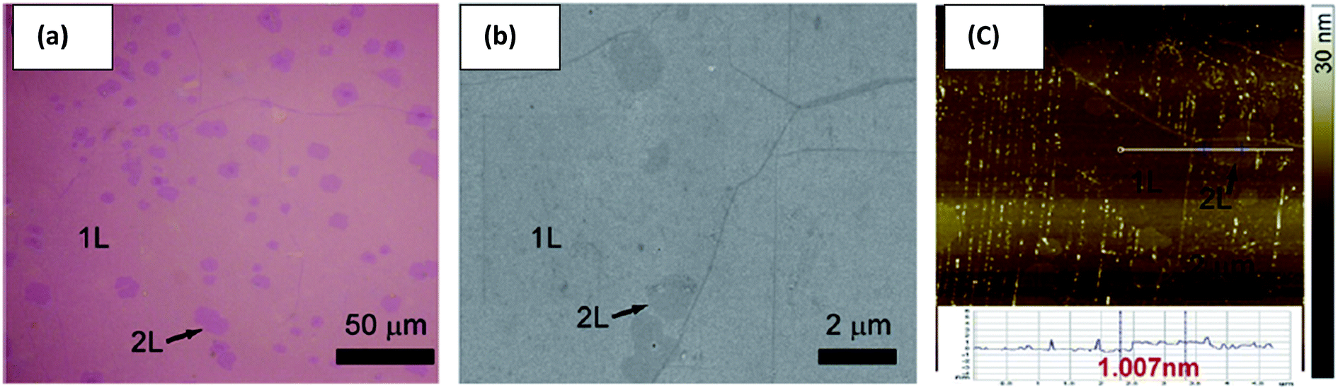
On the other hand, graphene films can be also synthesized using solid waste. Sharma et al.27 utilized solid waste plastic rich in polyethylene and polystyrene-based polymer components. The pyrolysis of waste plastic can generate polymeric components to provide the carbon source for the production of graphene layers. A highly crystalline monolayer graphene was characterized at four different points using Raman spectroscopy, as displayed in Fig. 3. The outcomes illustrated that the low and the high injection rates of polymeric components generated from the pyrolysis of the waste plastic could produce single-crystal and bilayer or few-layer graphene films, respectively. Moreover, big hexagonal and circle pattern single-crystal graphenes were produced successfully by controlling the pyrolysis rate of the waste plastic.
 | ||
| Fig. 3 Raman spectra of the transferred graphene crystal checked randomly at four different areas. Raman spectra show the high crystallinity of a monolayer graphene. This figure has been adapted/reproduced from ref. 27 with permission from Elsevier. | ||
In a similar study demonstrated by Ruan et al.,28 food, insects, and waste were promoted as carbon precursors to grow single graphene films. By using the waste to grow graphene layers, a novel method to transform waste materials into useful carbon product sparked a new idea in graphene synthesis. Furthermore, the quality of these product graphene layers produced from the waste was comparable with common carbon sources, such as methane.
Graphene growth via the CVD process remains a reliable way to produce graphene due to its scalability and potential to produce high-quality graphene film. However, it is an inefficient method as well because it requires high temperature.29 Therefore, by incorporating plasma into the CVD process of the production of graphene films, the production of graphene films could be realized under less stringent conditions, namely at a lower process temperature. Lee et al.29 successfully synthesized graphene sheets larger than a hundred nm2 in an area by using plasma-enhanced (PE)-CVD. Multi-wall carbon nanotubes (MWCNTs) were taken for a ball-milling process and graphene nanopowders were fabricated. Subsequently, the graphene nanopowders were utilized as the precursor of the PE-CVD process. Characterization then evidenced the presence of high-quality pure monolayer graphene sheets.
Besides the aforementioned solid carbon precursors, coronene30 and polycyclic aromatic hydrocarbon31 demonstrated their potential in the synthesis of high-quality graphene, with a very weak or negligible D peak observed.
2.2 Gas carbon precursors
Hydrocarbon gas precursors, such as methane, ethylene (reaction at 1000 °C)32–36 and acetylene (reaction at 650 °C)37 are among the most popular carbon sources used for synthesizing graphene.38 Among the gaseous carbon precursors, methane (CH4) is commonly used to synthesize graphene layers. For example, Lewis's group employed diluted CH4 gas to synthesize graphene on nickel films deposited over complete Si/SiO2 wafers, which was a great benefit for device fabrication.39 The results showed that a mixture of single-layer and few-layer graphene films were produced. Moreover, Chen and co-workers40 demonstrated the synthesis of high quality and excellent-crystallinity monolayer graphene sheets using CH4 as the carbon source. On the other hand, the fastest CVD graphene synthesis reported was produced using CH4 by Li's group,41 in which they successfully acquired continuous monolayer graphene films in 2 min at the reaction temperature of 1035 °C.Besides, CH4 can also be used in PE-CVD as the carbon precursor gas to synthesize single-layer graphene film. With using CH4 as the precursor gas and in the absence of a hydrogen gas flow, the production of monolayer graphene film on top of a Cu foil by PE-CVD was reported by Kim's group.42 It was found that the quantity of hydrogen species decomposed from the CH4 gas in the decomposition of the CH4 gas was sufficient for the single-layer graphene synthesis. Moreover, the plasma power of PE-CVD could affect the quantity of hydrogen species decomposed from CH4 gas. Thus, it was evidenced that CH4 acted not only as a carbon source for PE-CVD but also as a hydrogen gas source for the process.
By implementing plasma into the CVD graphene growth process, graphene growth could be conducted at a comparably lower temperature. For instance, Chan et al.43 successfully synthesized high-quality single-layer graphene film on a Cu foil at 600 °C using plasma-assisted thermal CVD. Various mixture fractions of hydrogen and methane gas precursors were investigated to produce graphene film via plasma-assisted thermal CVD. It was found that a high-quality graphene film could be synthesized by utilizing a high hydrogen concentration. In another study, a temperature as low as 450 °C was reported to grow a graphene layer on Ni foil via microwave plasma CVD (MPCVD) by Kim's group.44 A hydrogen and CH4 mixing ratio of 80:1 was used to obtain large-area monolayer graphene film. Single-layer graphene was produced by only using a short process time by using CH4 gas via radio-frequency PE-CVD, as demonstrated by Qi et al.45 It was found that the process time and the carbon precursor gas flow rate could directly influence the number of graphene layers produced. In conclusion, the CVD process assisted by plasma was able to synthesize good-quality graphene films at low temperature and low cost. In addition, the synthesis of graphene films for electronic device applications at low temperature is advantageous as a low temperature process in electronic device manufacturing is crucial.
Another type of hydrocarbon gas precursor that is widely used to synthesize graphene film is ethylene (C2H4). Addou and co-workers46 synthesized single-layer graphene films by ultrahigh vacuum (UHV) CVD using C2H4 as the precursor. Whereas CVD graphene growth is commonly conducted using a high temperature, in contrast to this, Addou and colleagues achieved monolayer graphene growth on nickel substrates at an optimum temperature of 550 °C, which is well below the graphene phase-stability temperature of 650 °C. Beyond this phase-stability temperature, the disintegration of the graphene layers may start, whereas at low temperatures (<500 °C), surface carbide will prevent the graphene layer from forming. In addition, Cazzanelli et al.47 also utilized ethylene as a carbon precursor by CVD to grow single-layer graphene film in high vacuum conditions on a platinum (Pt) substrate, which was thoroughly cleaned and properly oriented. It was reported that the monolayer graphene film synthesized was found to have two different orientations with respect to the Pt substrate used. Besides, Sagar's group48 investigated the formation of graphene film on different metal catalysts via the CVD process using C2H4 as the carbon precursor. It was found that by using similar experimental conditions, high-quality graphene films could be synthesized using a pressure of 0.2 MPa regardless of whether it was on copper or nickel foils.
Besides, by using acetylene (C2H2), Mueller and co-workers49 successfully achieved the synthesis of monolayer graphene film on copper foil by the route of UHV-CVD. The synthesized graphene film was comparatively high quality as compared to graphene film grown by low-pressure or atmospheric CVD. However, copper sublimation is a significant issue for using UHV-CVD process to produce graphene film. In another research, Woo et al.50 performed a completely uniform monolayer graphene synthesis on a metal thin film using C2H2 as the carbon precursor via inductively coupled PE-CVD (ICPCVD). By changing the metal substrate to doped alloys, a complete monolayer graphene film could also be grown using C2H2 as the gas precursor. It was found that the advantage of using Ni-doped copper alloy was that an even lower process temperature was needed compared to with the pure Cu substrate. It was suggested that Ni-doped bimetal alloy film might be a more economical alternative catalyst for complete monolayer graphene synthesis at low temperature.
Different types of metal foil have been used as templates to synthesize graphene for years, including the utilization of other types of templates such as quartz glass,51 mesoporous metal oxide,52–54 NaCl55 and 3D metal foams.56–59
The prepared 3D graphene foams consist of an interconnected graphene network, which acts as a channel for fast electron transport for high electrical conductivity.56–59 The measured electrical conductivity of graphene foam/poly(dimethyl siloxane) composites was ∼10 S cm−1 with loading as low as ∼0.5 wt%.58 The same results were obtained by Min et al.,59 who reported an electrical conductivity of 17.5 S cm−1 and a high specific surface area of 145 m2 g−1 because of the highly congested, porous and interconnected structure. Furthermore, the graphene foam also demonstrated good stability in stretching, bending and folding tests.59
Besides, the porous graphene network formed by using mesoporous metal oxide has a high specific surface area of 1448 m2 g−1 and a mesopore volume of 2.40 cm3 g−1, which serves as a pool of irons or active materials in electrochemical energy storage applications.52 In addition, Tang et al.53 and Zhao et al.54 demonstrated that hierarchical porous graphene is a suitable candidate for the cathodes of lithium–sulfur batteries. After 1000 cycles test, high reversible capacities of ca. 530 mA h g−1 and 380 mA h g−1 remained at 5 C and 10 C, respectively.54 However, a capacity of 434 mA h g−1 with an ultraflow cyclic fading rate of 0.11% for 150 cycles was achieved at a current density of 0.5 C, as reported by Tang et al.53
2.3 Liquid carbon precursors
Liquid precursors have attracted the interest of many researchers60,61 due to the liquid precursors being more available and more economical compared to hydrogen gas precursors. Liquid carbon sources, such as benzene,62,63 methanol64 and ethanol,65 have been employed as carbon sources to synthesize good-quality graphene film using CVD. Gadipelli et al.64 utilized benzene and methanol to grow graphene films on copper foil. It was shown that by using these liquid carbon precursors, the usage of large amounts of explosive gas, like methane and hydrogen, can be omitted, since hydrogen, CO and methane can be produced during the catalytic decomposition of methanol. Hence, in this way, the safety of the personnel carrying out the experiment is guaranteed. Besides, methanol is also found to be an inhibitor of amorphous carbon growth.Guermoune's group66 demonstrated various alcohols as liquid carbon precursors to produce good-quality monolayer graphene on copper foils by CVD. A comparison was done on the quantity and quality of the monolayer graphene films that were synthesized at a reaction temperature of 850 °C and duration of 5 min, using different types of alcohol, namely ethanol, propanol and methanol as well as methane gas. The quality of the graphene films produced using the alcohol precursors were on a par with that of graphene films synthesized using CH4, as shown in Fig. 4(a). Ethanol is one of the most common liquid carbon sources that are widely used to synthesize monolayer graphene films. In current research, Lisi and colleagues67 explored the feasibility of using ethanol as a carbon precursor in the synthesis of graphene, and found it promoted a fast growth rate in graphene synthesis. The results showed that a monolayer graphene sheet was synthesized and that it fully covered the whole copper substrate surface after exposing it at a low pressure of ethanol in the reaction time of 20 s. By comparing ethanol to other regularly used liquid precursors, ethanol appears to be a more efficient carbon precursor. The use of ethanol in graphene synthesis can be an advantage for industrial production, as it avoids the use of hazardous gas lines and pressurized cylinders because ethanol is very safe and inexpensive.
 | ||
| Fig. 4 (a) Comparison of the Raman spectra for graphene film synthesized by methanol, ethanol and 1-propanol. This figure has been adapted/reproduced from ref. 66 with permission from Elsevier. (b) Raman spectra of single (black and blue lines for 2-phenylethanol and ethanol, respectively), bi (green line) and tri (purple line) layer graphene. This figure has been adapted/reproduced from ref. 61 with permission from Elsevier. | ||
In another research conducted by Campos's group,61 the application of 2-phenylethanol and ethanol to produce monolayer graphene were demonstrated. They disclosed that monolayer graphene synthesized using ethanol covered a greater area of the substrate and had greater continuous layer formation, as well as a shorter synthesis time compared to that of 2-phenylethanol, as shown in Fig. 4(b). Furthermore, it led to a bigger dimension of monolayer graphene synthesized from ethanol in comparison with the graphene flakes. In addition, decomposition of benzene at a very low reaction temperature of 300 °C to synthesize graphene films was also demonstrated by Li et al.63 Although, a larger size of graphene flakes could be formed at a growth temperature of 500 °C, high-quality single-layer graphene flakes could be achieved at a reaction temperature of 300 °C when benzene was used as the liquid precursor.
Besides, a novel carbon precursor, namely hexane, has been utilized in the synthesis of graphene films by Srivastava's group, in which a mixture of large areas and uniform and continuous mono- and few-layers graphene could be produced.68 This novel synthesis method could be used to synthesize doped graphene films by using different organic solutions comprising dopant atoms.
3 Other synthesis methods of graphene
3.1 Thermal annealing
Besides the CVD method, monolayer graphene films have been recorded to be synthesized by many other approaches. Orofeo et al.69 reported that large-dimension, homogenous, monolayer graphene films could be produced by annealing amorphous carbon sputtered onto cobalt (Co)/sapphire and nickel (Ni)/sapphire substrates. Fig. 5 illustrates the schematic flow of the procedure to synthesize a graphene layer via the mentioned annealing amorphous carbon technique. The Co and Ni metal films sputtering on the sapphire substrates was validated as the key step to improving the crystallinity of the metals and assisting the formation of single-layer graphene. This was because highly crystalline substrates with less grain boundaries can promote the formation of a monolayer graphene film. Moreover, Carlo's group also evidenced that the cooling rate had no influence on the uniformity of monolayer graphene layer in comparison to the ordinary synthesis method using CVD and polycrystalline metal substrates. | ||
| Fig. 5 Schematic of the graphene growth process. (a) A thin metal film (∼200 nm) of Co or Ni is sputtered on a c-plane sapphire substrate at high temperature (∼500 °C) to produce a crystalline metal substrate. (b) After cooling down to room temperature, a thin layer of amorphous carbon (a-C) was sputtered on top of the metal film. The substrate was then annealed after reaching a vacuum pressure of ∼3.0 × 10⁻⁴ Pa using the process steps in (c). (1) The a-C/metal/sapphire was rapidly heated to the annealing temperature (750–800 °C) for 1.5 min. (2) The substrate was then kept at the peak temperature for 5–10 min. At this point, the a-C is expected to dissolve into the metal film. (3) After staging, the substrate was then cooled down at a controlled rate. (d) After annealing, graphene is formed on the surface of the metal, followed by transfer onto SiO2/Si (e) for further analyses. This figure has been adapted/reproduced from ref. 69 with permission from Springer. | ||
Li et al.70 successfully produced a mixture of mono- and few-layer graphene films by using annealing of a Co film deposited on a SiC substrate at 900–1000 °C, subsequently fast cooled in a water bath. The graphene layer was formed by the diffusion of free carbon from the SiC substrate in the rapid cooling process after Co reacted with Si. It was found out that the optimal conditions for monolayer graphene could be obtained by varying the Co film thickness, the annealing temperature or duration, and the cooling rate of the Co/SiC substrate after annealing.
3.2 Unzipping CNTs
Another technique to synthesize a graphene layer is to unzip single-walled carbon nanotubes (SWCNTs). A carbon nanotube (CNT) is actually a rolled-up graphene layer, therefore unzipping a carbon nanotube can yield a thin elongated strip of graphene, which is called a ‘graphene nanoribbon’. Recently, Tanaka et al. have fabricated single-layer graphene nanoribbons (sGNRs) by utilizing double-walled carbon nanotubes (DWCNTs). Instead of using MWNTs, Tanaka and colleagues71 found that DWNTs are better precursor material to be unzipped to form GNRs. Fig. 6 illustrates the unzipping process of DWNTs to form sGNRs. Initially, defects were induced in the DWNTs by annealing them in the air at 500 °C, followed by dispersing them in an organic solution. Before the dispersed DWNTs were unzipped into high-quality double-layer (d)-GNRs, they were subjected to sonication treatment. After that, the dGNRs were further sonicated in order to form sGNRs individually. Those steps produced sGNRs, which are crucial for the advancement of graphene-based electronics. | ||
| Fig. 6 Method of synthesizing single-layer graphene nanoribbons (sGNR) from double-walled carbon nanotubes (DWCNTs). This figure has been adapted/reproduced from ref. 71 with permission from Nature Publishing Group. | ||
3.3 Solvothermal
The solvothermal synthesis method is another way to produce single-layer graphene film. To obtain sodium ethoxide, ethanol and sodium were used as the carbon precursors for the solvothermal process in the rapid pyrolysis of sodium ethoxide to yield a graphene layer.72 Besides, Singh et al.73 synthesized graphene layers using the thermal decomposition of ethyl alcohol. The produced graphene layer was investigated using high resolution transmission electron microscopy (HRTEM) to confirm its high quality after purification. Furthermore, AFM analysis was conducted on the synthesized graphene sheets and showed that a mixture of monolayer to trilayer graphene sheets was produced. Therefore, the solvothermal method is a viable process to produce single-layer graphene film, which makes it a quite attractive method due to its comparably safer and cheaper process than other methods.3.4 Electrochemical
It is very interesting when another electrochemical route was reported Alanyalıoğlu et al.,74 who synthesized graphene films with a thickness near to monolayer by using two steps: the electrochemical intercalation of sodium dodecyl sulfate (SDS) into graphite and the electrochemical exfoliation of the SDS-intercalated graphite, as shown in Fig. 7. The features of the produced graphene sheets were greatly affected by the value of the electrode potential for the electrochemical intercalation of SDS into graphite layers, for example, the number of graphene layers, dimension and the structural order. It was found that the intercalation process could only take place when the electrode potentials were higher than 1.4 V, while a strong intercalation potential was used to produce monolayer graphene films. The intercalation method has an advantage to the exfoliation process because it can avoid the individual exfoliated graphene sheets restacking again in the solution by having surfactants adsorbed on the surface of the graphene films. Therefore, the successful production of a huge volume of reduced structured graphene films could be a new path targeted by scientists for various applications. | ||
| Fig. 7 Schematic of the electrochemical route to produce a graphene/SDS suspension. This figure has been adapted/reproduced from ref. 74 with permission from Elsevier. | ||
Yu et al.75 employed highly oriented pyrolytic graphite (HOPG) as a carbon source to exfoliate graphene from HOPG with a size of about 510 nm2 using the electrochemical exfoliation technique. Fig. 8 illustrates the schematic of the circuit connection of HOPG. HOPG was attached to a tungsten wire by a silver pad and then it was inserted into the electrolyte as the anode of the circuit. A platinum (Pt) sheet was used as the cathode of circuit in parallel with the HOPG. The electrochemical exfoliation method successfully synthesized nanometre-size and high-quality single-layer graphene. This developed technique is important for the realization of conductive film for fuel cell applications.
 | ||
| Fig. 8 Schematic of electrochemical exfoliation. This figure has been adapted/reproduced from ref. 75 with permission from The Materials Research Society of Japan. | ||
3.5 Thermal decomposition
SiC has been widely used to grow carbon-based materials even before graphene's discovery in 2004.76 A single-crystal SiC substrate was heated up to a high temperature of more than 1000 °C in an ultrahigh vacuum chamber to prompt the sublimation of silicon (Si) atoms on the SiC surface. Following the sublimation of Si atoms, the subsequent graphitization of the surplus carbon atoms could occur on the surface of the SiC substrate,77 and thus, graphene films were formed. Yu and colleagues78 developed a novel way to produce high-quality epitaxial graphene sheets, named the ‘face-to-face’ method. An illustration of the face-to-face growth design model is shown in Fig. 9. Two SiC substrates were fixed on top of the other SiC substrates surface with a small gap of 25 μm in between them. During the graphene growth process, both the SiC substrates were heated simultaneously. By using the heating temperature of 1530 °C and governing the Si sublimation rate, the carbon atoms were reconstructed to form single-layer graphene. AFM measurements showed that the uniformity of the graphene was enhanced by using the face-to-face synthesis technique as compared to the traditional decomposition approach. | ||
| Fig. 9 Schematic view of the configuration of the face-to-face growth method. This figure has been adapted/reproduced from ref. 78 with permission from Elsevier. | ||
3.6 Ball-milling exfoliation
In addition, single-layer graphene layer has been synthesized using a ball-milling exfoliation method by Del Rio-Castillo et al.79 This unique ball-milling exfoliation method is a simple, cheap and eco-friendly way to obtain high-quality graphene layers. Antonio's group used melamine (melamine: 2,4,6-triamine-1,3,5-triazine) as the exfoliating agent and carbon fibres as the carbon precursor material. The addition of a small amount of solvent during the ball-milling process of carbon fibres greatly enhances the exfoliation process, therefore allowing the dispersion of single-layer graphene. In addition, they also demonstrated the use of Hansen solubility parameters to differentiate between single-layer graphene and poorly exfoliated fibres. This method offers an easy, inexpensive and expandable production technique to synthesize monolayer graphene.3.7 Calcination
Besides, Wang and colleagues80 reported the successful synthesis of monolayer graphene sheets using zeolite Ni-MCM-22. It was the first time they used zeolites as a catalyst and template. The synthesized graphene layers had a high electrical conductivity of 73.6 S m−1 (much higher than graphene synthesized by solvothermal synthesis at 0.05 S m−1 (ref. 72) and by chemically reduced synthesis at 0.05–2 S m−1 (ref. 81)), manageable 2D sizes and a big surface area, and consequently have been applied successfully as electrodes in supercapacitors. They have also demonstrated superior electrochemical double-layer capacitance and galvanostatic charge/discharge properties with specific capacitances of 233 F g−1 in aqueous KOH. Fig. 10 illustrates the growth processes of a graphene sheet. The benefit of this practice is that the zeolite MCM-22 could influence the number of as-produced graphene layers. In addition, the size distribution of the MCM-22 nanosheets (50–820 nm) were very close to the 2D graphene sizes (65–650 nm) due to the template effect. Therefore, with its excellent electrochemical capacitance properties, the synthesized graphene was suitable for use in supercapacitors. | ||
| Fig. 10 Schematic of the preparation process of a graphene sheet from MCM-22. This figure has been adapted/reproduced from ref. 80 with permission from Elsevier. | ||
3.8 Irradiation of highly charged ions
Besides, monolayer graphene produced on the HOPG surface has been reported by Peng et al.82 Here, HOPG basal surfaces were bombarded by highly charged xenon, Xeq+ (q = 5, 21, 26), ions to modify the solid surface. The large potential energy carried by Xe ions can be deposited onto the HOPG surface and eventually modifies the solid surface and leads to the nano-sized structure. Peng and co-workers compared the Raman results of synthesized graphene layers in term of different charge states of the Xe ions and different irradiation doses of 8 × 10¹², 3 × 10¹³, 1 × 10¹⁴ and 3 × 10¹⁴ ions per cm2. It was found that bombardment using Xe5+ onto the HOPG surface tended to form monolayer graphene more than when using other Xe ions. On the other hand, it was observed that using a higher irradiation dose of Xe ions effectively destroyed the graphite structure and no monolayer graphene was formed. Therefore, monolayer graphene was easier to be synthesized by the effect of reduced charged state ions with lower doses. This novel method could pave a way for more variety in the ways of graphene production in the future.Apart from HOPG used as the template, the use of nickel for the deposition of Zn and Bi to synthesize single-layer graphene was demonstrated by Aminalragia Giamini and co-workers.83 They showed that Zn and Bi altered the surface of nickel, prohibiting the growth activity of multilayer graphene. Thus, a low temperature of 600 °C was used to grow high-quality single-layer graphene, which indicated a much better enhancement compared with bare nickel.
3.9 Epitaxial growth
On the other hand, a composition of metal deposited on a HOPG could be a new type of catalyst for the synthesis of graphene films. It was reported by Xu and colleagues,84 whereby the deposition of nickel film on the surface of a HOPG substrate was done prior to the synthesis of monolayer graphene at reduced temperature. The synthesized monolayer graphene has uniform thickness and covered ca. 100% of an entire 2 cm × 2 cm nickel substrate. Similar to CVD, carbon species diffused out from HOPG substrate via the nickel substrate during the annealing process and precipitated on the nickel substrate to form single-layer graphene sheets. However, in order to achieve a graphene layer with a well-controlled thickness and crystal structure, the annealing temperature and time were the crucial parameters optimized to control the quantity of carbon atoms for the synthesis of monolayer graphene sheets.The epitaxial growth of single-layer graphene is not a new technique nowadays. It was demonstrated by Gao et al.85 using a surface segregation technique. X-ray photoelectron spectroscopy (XPS) revealed the interaction between graphene and Pd(111) is very weak, where no charge transfer occurs. Gao and co-workers found that, a high annealing temperature of more than 820 °C inhibited the formation of graphene as the majority of carbon atoms had dissolved into the Pd substrate. Furthermore, a thermal decomposition of C60 on copper by using supersonic molecular beam (SuMBE) epitaxy at a reaction temperature of 645 °C (below the conventional graphene synthesis CVD temperature of 1000 °C) was demonstrated. The researchers found that a high kinetic energy affects the synthesis of graphene and could occur with several types of metallic or semiconductor substrates at lower synthesis temperatures.86
3.10 Mechanical exfoliation
Andrei Geim and Kostya Novoselov separated a graphene layer from HOPG for the first time using a mechanical exfoliation method 2004.3 However, the disadvantage of this method was that only a tiny surface area of the single-layer graphene film could be acquired. Thus, Shmavonyan et al.87 successfully produced a larger surface area of monolayer graphene by additionally cleaving few-layer graphene near the monolayer region. After the additional cleaving, the surface area of the synthesized single-layer graphene was significantly enlarged, as depicted in Fig. 11. The AFM results of the produced single-layer graphene also showed a height of 0.66 nm, which was in agreement with the theoretical thickness of single-layer graphene sheets.3 | ||
| Fig. 11 Optical images of: (a) as-prepared (by Scotch tape method) and (b) enlarged (by suggested method) monolayer graphene. This figure has been adapted/reproduced from ref. 87 with permission from National Academy of Sciences of Armenia. | ||
3.11 Liquid-phase exfoliation
The production of a graphene layer through the liquid-based exfoliation of graphite is typically a promising technique for large-scale graphene synthesis.88 Previously, Zhu's group89 successfully synthesized large-scale, good-quality graphene nanosheets through the liquid-phase exfoliation of graphite in a solvent of N,N-dimethylformamide (DMF) and water. By using DMF as well, Liu et al.90 utilized supercritical DMF to exfoliate expandable graphite into few-layers graphene and then repeated the same procedure to exfoliate the few-layer graphene into monolayer graphene. A supercritical fluid possesses a pressure and temperature above its critical point, where it does not exist in distinct gas or liquid phases.91Fig. 12 illustrates the process flow for fabricating monolayer graphene by using supercritical DMF exfoliation. It was found that the optimum process parameters to produce graphene layer were a concentration of 2 mg ml−1, at a temperature of 673 K, and with a volume ratio of DMF of 0.67. The produced graphene sheets had less defects than other chemical methods reported, which indicates the high quality of the resultant graphene layers. Therefore, this method is inexpensive, simple to scale up and generates less toxic waste as compared to the reduction of graphene oxide (GO) via the chemical route, which involves hydrazine hydroquinone and dimethylhydrazine. In addition, graphene layers have been synthesized by using a graphite dispersion in aqueous surfactant solutions. Yumin's group92 reported ultrasonic-dispersed graphite flakes in sodium cholate and polyoxyethylene nonylphenyl ether aqueous solution and consequently, ultra-centrifugation of the solutions was carried out. The Raman and AFM results revealed that the graphene samples were in single-layer and few-layers graphene. However, further research on the size control needs to be conducted to improve the dimensions of the synthesized graphene sheets.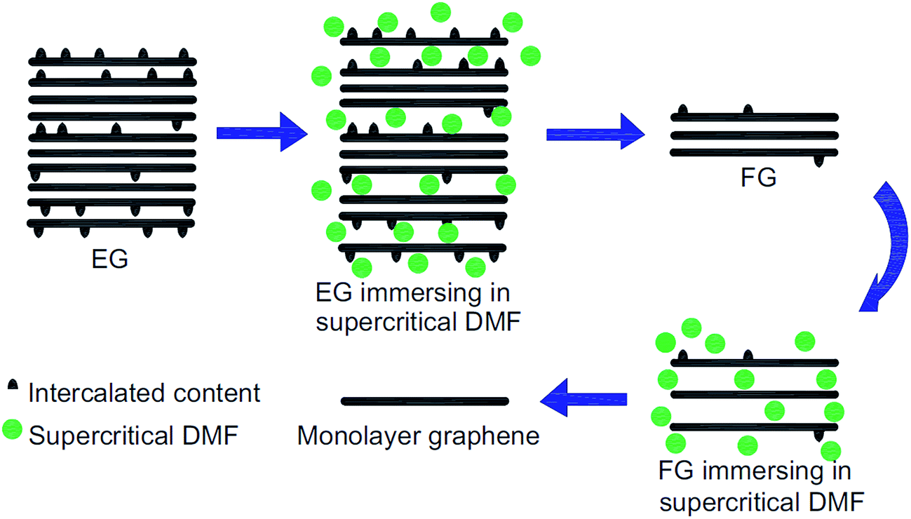 | ||
| Fig. 12 Schematic of the fabrication of a few-layer graphene (FG) and monolayer graphene by exfoliation of expandable graphite (EG) in supercritical DMF. This figure has been adapted/reproduced from ref. 90 with permission from Elsevier. | ||
In another liquid exfoliation process, Chen et al.93 demonstrated the high production of monolayer graphene micro-sheets with controlled dimensions using a simple hydrothermal treatment of GO sheets. The addition of a polymer, like poly(vinyl pyrrolidone) (PVP), can weaken the interaction between the micro-sheets and prevent the aggregation of graphene micro-sheets during the reduction process. Besides, the addition of PVP could preserve the morphology of the synthesized graphene micro-sheets as well. The dimensional control of the graphene micro-sheets produced was achieved by manipulating the reaction temperature. Thus, the synthesis of micro-sheets with desired sizes shows promising potential for application for high-performance polymer composites due to the high yield and cost-effective process.
3.12 Thermal exfoliation
Korobeinyk and colleagues94 reported a facile process for the simple production of carbon nanomaterials by carbonization of a co-polymer. In the carbonization of polyacrylonitrile (PAN) co-polymer, a mixture of carbon nanofibres and mono- and multilayer graphene were produced. The co-polymer was initially subjected to heat treatment, and during the carbonization stage, shrinkage of the monolith occurred, which led to exfoliation to form single- and multilayer graphene. The AFM results depicted that the height of the individual graphene flake was consistent with the previous report.95 This non-catalysed growth of carbon nanomaterial offers an alternative route for graphene synthesis at lower cost and causes only a small amount of damage to the produced nanomaterial.4 Transfer of graphene
CVD has been most widely employed among several synthesis approaches for high-quality graphene because of its advantages, such as being able to produce large-area and high-quality graphene at economical cost. Applying CVD-grown graphene to electronic applications, a transfer process is needed to move the graphene film to the dielectric substrates from the catalyst it was synthesized on. In recent years, besides the advancement in graphene synthesis, advancements in the transfer methods onto the target substrates have also been reported. The methods are classified into mechanical exfoliation,3 polymer-assisted transfer96–99 and continuous transfer by a roll-to-roll process,100,101 as well as transfer-free methods, including the direct synthesis on the dielectric substrates.102,103 All graphene transfers involve the use of chemicals, with the experiments conducted in dry or wet conditions. Thus, we categorized all the methods into two different types: wet chemical and dry chemical methods.4.1 Wet chemical methods
The first proposed approach for graphene transfer was the widely used method of etching a metal substrate called the ‘wet transfer method’. The transfer process is generally conducted by coating a protective layer of polymeric polydimethylsiloxane (PDMS) or PMMA over the graphene film, followed by etching of the underneath substrate, such as copper, in etching solvents. There are many types of etching solvents, such as iron chloride (FeCl3), hydrochloric acid (HCl), nitric acid (HNO3), iron(III) nitrate (Fe(NO3)3 and copper chloride (CuCl2).Apart from this method, Her et al.104 presented a new graphene transfer procedure using acetic acid, which could removed the residue that was commonly found in standard acetone treatments. Fig. 13 presents a comparison of the applications of acetic acid and acetone methods to etch SiO2. In both methods, the same graphene transfer procedure was used, but the etching solvent was different. Fig. 14 displays the comparison results between the acetone- and acetic acid-based transfer methods characterized by light microscopy, AFM and Raman spectroscopy. There was no obvious folding or tearing in the graphene layer on either of the transfer methods. Therefore, a very clean graphene surface can be yielded with these relatively simple graphene transfer methods. They also produced defect-free graphene surfaces, which could be deposited on various target substrates for different applications.
 | ||
| Fig. 13 Schematic of graphene transfer. PMMA was deposited on a graphene layer and cured at 115 °C for 2 min. The graphene–PMMA stack was then detached from the substrate in a sodium hydroxide bath and subsequently deposited on a target substrate. Finally, the PMMA was dissolved using acetone or acetic acid and then rinsed in a mixture of methanol and water. This figure has been adapted/reproduced from ref. 104 with permission from Elsevier. | ||
 | ||
| Fig. 14 Comparison of graphene transfer methods. (a), (c) and (e) Standard acetone-based approach and (b), (d) and (f) acetic acid method. The images show a graphene sample that has been transferred onto a glass substrate. (a) and (b) Optical images viewed under a differential interference contrast (DIC) light microscope. (c) and (d) Topographic images recorded with AFM, and (e) and (f) Raman spectra. The red box indicates the D band frequency range. This figure has been adapted/reproduced from ref. 104 with permission from Elsevier. | ||
Lin et al.105 demonstrated the transfer of a large-scale graphene film to a target substrate by using a novel technique without polymer, which resulted in a product with better properties compared to the conventional polymer-assisted methods. Fig. 15 illustrates the process flow to prepare a large-area single-layer graphene film, which could be directly deposited on any substrate for further application. A mixed solution of isopropyl alcohol (IPA) and 0.1 M ammonium persulfate solution ((NH4)2S2O8) at a ratio of 1:10 was used as the etchant to etch the copper substrate. Single-layer graphene film floated on top of the solution after the copper substrate was etched by the mixed solution. The etchant was then substituted by a mixture of DI water and IPA in order to control the surface tension. The floating graphene film was then transferred to the desired substrate and it was found that the resultant graphene film was free of organic residues.
 | ||
| Fig. 15 Schematic of the polymer-free transfer process. This figure has been adapted/reproduced from ref. 105 with permission from American Chemical Society. | ||
In another research report, Barin's group106 studied the effects of varying the parameters of each step in the transfer method using PMMA polymer on the end product features, such as structure and electrical properties. It was found that by using double layers of PMMA deposition, a better quality of transferred graphene layer could be achieved. The time for the post-baking process of the transferred graphene layers was also crucial in influencing the condition of the graphene films; whereby a shorter baking time of the graphene films of around 5 min resulted in cracks and wrinkles on graphene layer during PMMA etching, because of the insufficient time for the dissolution of the leftover water content between the graphene film and the substrate. However, a longer period of baking time resulted in a greater quantity of residues of PMMA on the surface of graphene film. AFM images of samples with a PMMA layer baked with various different parameters are shown in Fig. 16.
 | ||
| Fig. 16 AFM images of graphene films baked during: (a) 5 min at 80 °C, (b) 5 min at 80 °C + 20 min at 130 °C and (c) 5 min at 80 °C + 40 min at 130 °C. This figure has been adapted/reproduced from ref. 106 with permission from Elsevier. | ||
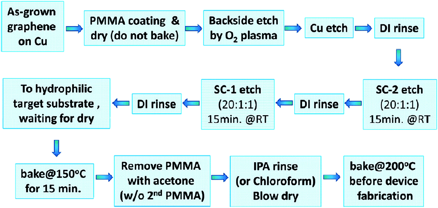
Liang's group107 developed a simple modified RCA clean transfer technique to remove Cu and/or Fe residues, which are very hard to be cleaned off thoroughly using traditional transfer techniques. In this method, control of the hydrophilicity of the targeted substrates and baking was combined with the efficient modified RCA clean process to reduce the amount of cracks and the impurity level of the transferred graphene. Fig. 17 displays the process flow of the simple modified RCA clean process. This demonstration proved a big leap forwards toward large-scale graphene-based electronic device applications.
 | ||
| Fig. 17 Simple ‘modified RCA clean’ graphene transfer process flow. This figure has been adapted/reproduced from ref. 107 with permission from American Chemical Society. | ||
A new novel graphene transfer method involving reverse transfer onto target substrates was developed by An's group.108 Compared to conventional approaches, this novel method performs better in terms of the density of cracks in the graphene and the impurity levels. Fig. 18 illustrates the overall schematic diagram for the fabrication of graphene by using this new novel transfer method. The process flow of the mentioned transfer method is similar to conventional methods. After the copper catalyst was thoroughly etched away by FeCl3 etchant, the bilayer comprising the PMMA/graphene was cleaned with pure water. The PMMA-coated graphene was reversely located on the desired substrate against the side of PMMA. Consequently, no extra process to discard PMMA film was needed in this PMMA reverse transfer technique. In contrast, the PMMA film in between the graphene layer and polyethylene terephthalate (PET) flexible substrate increased the adhesion of the graphene onto the substrate. Furthermore, the layer-by-layer assembly technique is effective to avoid the aggregation of PMMA residue accumulation between graphene layers before they are transferred onto flexible substrates, as testified by Cheng's group.
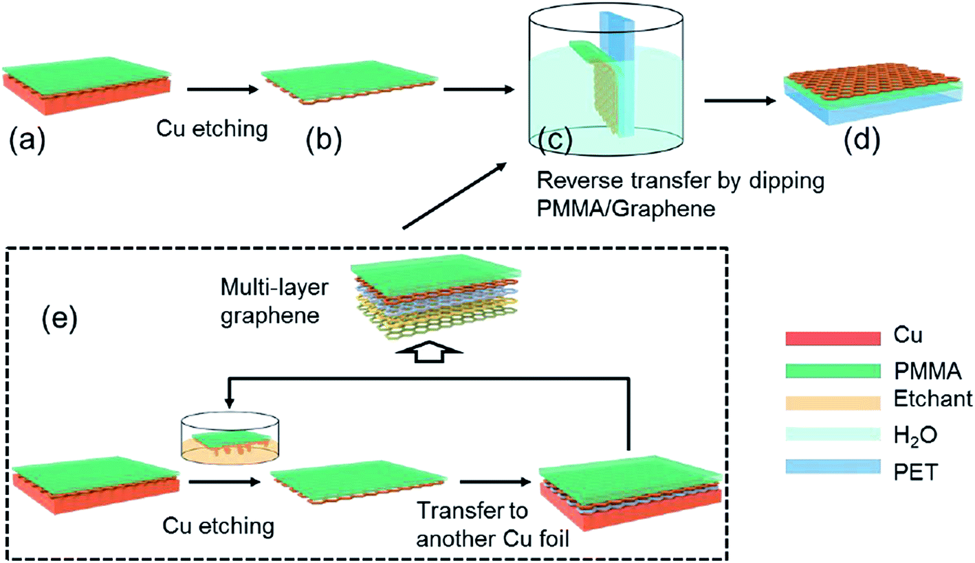 | ||
| Fig. 18 Graphic drawing of the PMMA reverse transfer process. (a) PMMA was spin-coated onto CVD-grown graphene, and (b) the copper underneath the graphene was completely removed by an etchant (c) after cleaning with pure water, the PMMA-coated graphene was transferred in a reverse manner onto flexible substrates, (d) with a stacking order of graphene–PMMA–substrate. (e) The layer-by-layer assembly method was used for fabricating multilayer graphene. This figure has been adapted/reproduced from ref. 108 with permission from The Royal Society of Chemistry. | ||
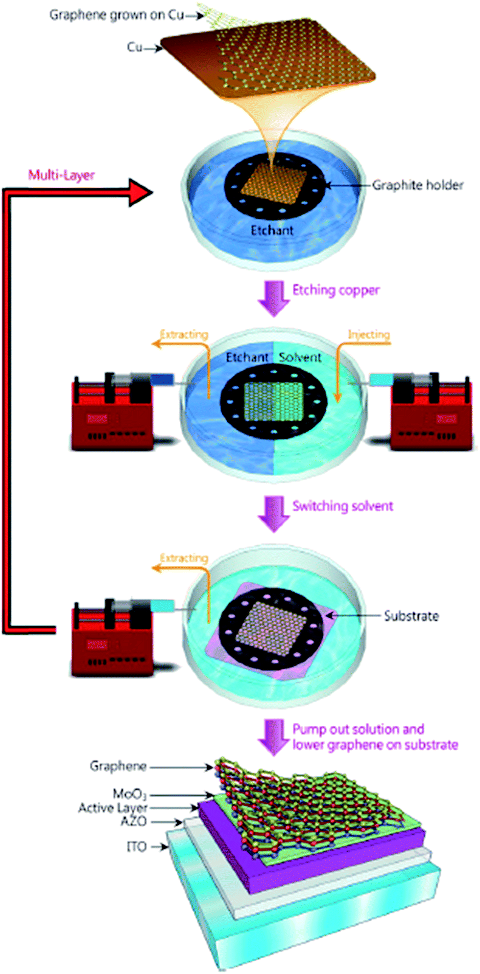
The direct growth and easy transfer method on a new substrate is highly important for semiconductor production lines, such as for the production of transistors, optoelectronics modulators, on-chip biosensors and tunnelling barriers.109–111 Therefore, Gao and co-workers112 invented a novel face-to-face transfer method, in which graphene film was grown in a wafer-scale and then transferred one wafer at a time. This transferring approach depends on the formation of nascent gas bubbles and capillary bridges between the graphene–substrate interfaces during etching of the underlying metal substrate. Compared to the previous studies on wet96,98,113–115 or dry100,116 transfer methods, this novel approach can synthesize graphene layers with a much lower density of transfer defects. Fig. 19 shows the schematic drawing of the comparison of the process with and without ‘bubble seeding’ by plasma treatment. During the metal substrate etching process, plasma pre-treatment of the substrate facilitates the capillary bridges to form, which result in the synthesized graphene film remaining attached on the substrate without undergoing delamination. The etching of the copper substrate caused the copper to dissolute and created voids and channels, which allowed the infiltration of the liquid etchant in between the synthesized graphene film and the underlying substrate. Graphene is hydrophobic in nature, in which an instability of the planar interface can be produced between the soft graphene film and water molecules. Thus, capillary bridges in between graphene–substrate interfaces were formed by the assistance of the emergence of bubbles during the etching process of the metal substrate. Therefore, the plasma pre-treatment played a vital role in transferring the graphene film. In Fig. 20, the as-synthesized graphene before transfer shows an insignificant D band, which indicates nearly no defects are present. On the other hand, both the float-transferred and face-to-face transferred graphene display minor D peaks, where the face-to-face transferred graphene has a higher 2D band than that of the float-transferred graphene, indicating its higher crystalline quality.
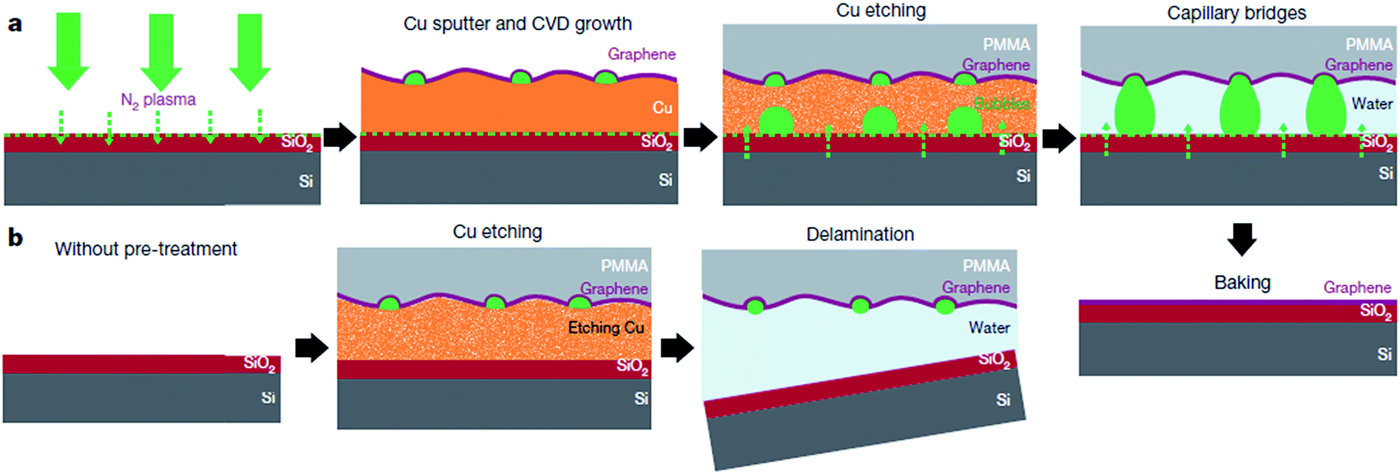 | ||
| Fig. 19 Interpretation of the face-to-face technique for transferring graphene mediated by capillary bridges. (a) Schematic drawing showing the ‘bubble seeding’ by plasma treatment, CVD growth, Cu film etching, formation of capillary bridges and removal of water and PMMA. (b) Schematic illustration showing that in the absence of plasma treatment, delamination of the film results. This figure has been adapted/reproduced from ref. 112 with permission from Nature Publishing Group. | ||
 | ||
| Fig. 20 Raman spectra of graphene prepared by the face-to-face technique and by float transfer onto SiO2/Si substrates, and of graphene onto Cu film before transfer. This figure has been adapted/reproduced from ref. 112 with permission from Nature Publishing Group. | ||
Apart from this method, Kafiah et al.117 utilized polypropylene (PP) and polyvinylidenedifluoride (PVDF) as target substrates to transfer a graphene film for water desalination. In order to transfer graphene onto the target substrate, their process involved the wet etching of a copper substrate after the grown graphene film was attached onto the target substrate. They found out that a low surface roughness, small pore size and fairly high hydrophobicity assisted the smooth and uniform transfer of the monolayer graphene film onto the polymer membranes. Fig. 21 displays the schematic flow of the transfer of the monolayer graphene film onto the polymeric substrate. This graphene transfer method applied ammonium persulfate (APS) as the copper etching agent to dissolve and remove the copper. Defects and tears of the transferred graphene can be sealed via interfacial polymerization using Nylon 6,6 to improve the blockage of the ions during the water desalination process.
 | ||
| Fig. 21 Schematic of single-layer graphene transfer onto a polymeric substrate. This figure has been adapted/reproduced from ref. 117 with permission from Elsevier. | ||
Many researchers have utilized PMMA as the substrate to hold the graphene film while the underneath copper substrate was etched away. However, Chandrashekar et al.118 and Gupta, P. et al.119 demonstrated a successful graphene transfer with the help of boiled distilled water. Hailin Peng et al.118 reported that the copper foil was oxidized faster when the Cu/graphene/EVA/PET film was immersed in hot water. Moreover, the formation of an oxide layer reduces the surface energy of copper and eases the water infiltration by modifying the copper foil from hydrophobic to hydrophilic.120,121 Therefore, they believed that the adhesion force of graphene and copper in hot water was weakened and thus, the delamination of graphene from the copper foil was facilitated.
4.2 Dry chemical methods
There are also some new novel techniques to transfer synthesized graphene film onto desired substrates for particular application purposes. In one experiment, Yang et al.122 transferred graphene film by the direct delamination technique from a metal substrate and, in turn, eliminated the need for the conventional metal etching process. This can overcome the issues such as the risk of physical damage to the graphene during the etching process. In detail, Yang's group immersed the CVD-synthesized graphene film onto a metal substrate into aqueous poly(vinyl alcohol) (PVA) solution to form a PVA film, which could act as a carrier to hold the monolayer graphene during the transfer process. Fig. 22 compares the optical microscopy (OM) pictures of the transferred graphene on a silicon substrate for with and without pre-treatment of the graphene growth substrate in PVA solution. Yang and co-researchers found that the transfer process with pre-treatment yielded graphene film with a more continuous and almost void-free features than the graphene film without pre-treatment. Thus, this depicts that the PVA pre-treatment step plays a critical role in achieving a clean delamination of the graphene layer. | ||
| Fig. 22 (a) Optical microscopy images of the transferred graphene on SiO2 (300 nm)/Si substrate with pretreatment in PVA solution and (b) without pretreatment. Inset in (a) shows a photograph of the target SiO2/Si substrate with the transferred graphene (left) and the growth substrate (Cu/SiO2/Si) after direct delamination of the graphene (right). The entire area of the growth substrate (1.5 cm × 1.5 cm) was used for the delamination of the graphene. The area and the shape of the growth substrate was preserved in the graphene transferred onto SiO2/Si. The purple colour in (b) indicates the fragmented, transferred graphene. This figure has been adapted/reproduced from ref. 122 with permission from Wiley-VCH. | ||
Besides, Ren et al.123 reported an enhanced transfer of graphene by immediate taking up of the graphene with desired substrates as compared to the conventional PMMA-based transfer technique. The Raman results showed that the graphene film synthesized by the direct transfer method was good quality in terms of the structure and no extra doping in the graphene layer. On the other hand, the PMMA-based transfer method introduces significant n-type doping in the graphene transferred. Fig. 23 displays a comparison of the Raman spectra of the direct transfer and PMMA-based transfer samples. The higher 2D/G peak ratio indicates a cleaner surface of graphene layer than the PMMA-based transferred samples.
 | ||
| Fig. 23 Raman spectra (532 nm laser excitation wavelength) for graphene transferred onto the SiO2-on-Si substrate. (a) Raman spectra obtained from a sample prepared by the standard PMMA-based method. (b) Raman spectra obtained from a sample obtained by the direct transfer method. This figure has been adapted/reproduced from ref. 123 with permission from World Scientific. | ||
In addition, Yang's group124 proposed a clean and effective transfer of graphene by the electrochemical etching of copper substrates, which preserved the quality of graphene. The continuous graphene films were transferred with less contamination and also unexpected p-type doping was demonstrated as compared with the typical wet-etching in oxidant solutions. Fig. 24(a–c) display the OM, SEM and AFM images of the transferred graphene film by the clean transfer method. The whole transferred graphene film was tidy and endless, as shown in the OM image in the Fig. 24(a). In agreement with the OM results, the SEM and AFM images in Fig. 24(b) and (c), respectively, demonstrate a smooth, continuous and flat monolayer graphene film without major cracks. Moreover, this technique was carried out under well-controlled oxidation potentials. The effects of different oxidation potentials on the quality of graphene was studied, as shown in the Raman spectrum in Fig. 25, in which the etching rate of Cu was obviously increased with increasing the oxidation potentials. At a voltage of more than 2.0 V, the D band was seen for the transferred graphene, which is in contrast to that observed with graphene electrochemically transferred at different potentials below 1.0 V.
 | ||
| Fig. 24 Characterization of graphene transferred by electrochemical oxidation. (a–c) Typical optical microscopy, SEM and AFM images of monolayer (1L) graphene electrochemically transferred onto a 300 nm thick SiO2/Si substrate, respectively. This figure has been adapted/reproduced from ref. 124 with permission from Elsevier. | ||
 | ||
| Fig. 25 Raman spectra of monolayer graphene films electrochemically transferred under different oxidation potentials, such as 0.3, 0.6, 0.8, 1.0 and 2.0 V. This figure has been adapted/reproduced from ref. 124 with permission from Elsevier. | ||
Fechine et al.125 demonstrated a direct dry transfer method to transfer large-surface-area graphene onto a few types of polymers. The transfer method was conducted using mild heat and pressure combined with mechanical peeling of the starting substrate without electrochemical delamination or chemical etching. Fig. 26 displays the schematic of the procedure to transfer the graphene onto the polymer film. The mechanical peeling of the metal foil from the polymer/graphene stack was conducted with moderate pressure and temperature after graphene on the Cu foil was placed in contact with the polymer film. This straightforward method did not need to use any extra material except for graphene on the metal foil and polymer film. It was also found that the key to manipulate the graphene transfer was by fine-tuning the graphene transfer conditions.
 | ||
| Fig. 26 Schematic of the transfer method and sample after transfer. (a) Graphene/metal and polymer film before transfer. (b) Polymer application step to form the metal/graphene/polymer stack. (c) Peeling of the metal step. (d) Final graphene/polymer stack. This figure has been adapted/reproduced from ref. 125 with permission from Elsevier. | ||
In addition, Martins and co-workers126 developed a method for the direct transfer of a graphene layer onto flexible bulk substrates via lamination. The transfer technique did not require any intermediate transfer membrane, which otherwise would have needed to be detached subsequently. Fig. 27 shows the schematic illustration of the direct transfer process via lamination, which involves lamination followed by chemical etching of the Cu substrate. To adhere the synthesized graphene sheet to the target substrate, the lamination was done before the etching process. A variety of targeted substrates were studied and their properties were compared, and two crucial factors were identified that could ensure a successful transfer: the substrate's hydrophobicity and a good contact between the substrate and graphene layer.
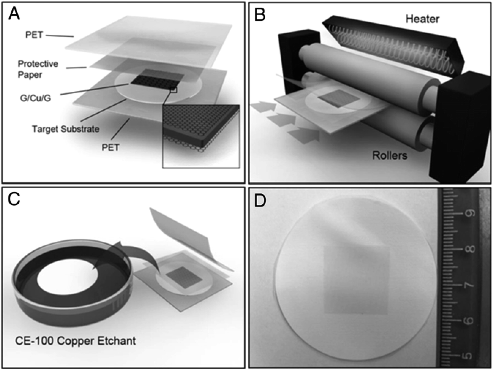 | ||
| Fig. 27 Schematic of the direct transfer technique via lamination. (A) Copper foil with CVD graphene grown on both sides is placed in between the target substrate and the protective paper. (B) The sandwich structure is inserted into the hot/cold lamination machine. (C) The PET films and the protective paper are then removed and the remaining substrate/graphene/copper stack is floated on a copper etchant solution for 15 min. (D) The graphene/substrate is rinsed in DI water and blow-dried with nitrogen. This figure has been adapted/reproduced from ref. 126 with permission from Proceedings of the National Academy of Sciences. | ||
In recent years, a dry transfer method using PDMS as a stamping polymer and a polyisobutylene (PIB) layer as the graphene-support polymer was reported by Milan et al.127Fig. 28 shows an illustration of the dry transfer technique using PIB as the support polymer. After the graphene film has been transferred to the target substrate, the PDMS stamp was detached, and then the PIB layer was dispersed in an aliphatic solvent, namely hexane. They found that the use of an aliphatic solvent does not degrade the quality of the targeted polymer substrate. Hence, this cheap, fast and clean graphene transfer approach is suitable to be used to transfer CVD graphene onto polymer substrates with high accuracy and large outputs. Moreover, this technique is beneficial to transfer graphene onto hydrophobic substrates. In another project by Song's group,128 graphene was transferred by using a sacrificial ‘self-releasing’ polymer layer placed between the PDMS stamp and the graphene film (Fig. 29). The self-releasing layer facilitated the delamination of the synthesized graphene film onto a new targeted substrate. The release layer possessed a smaller adhesion force with graphene than the targeted surface, which makes it advantageous. Besides, Song's group also proved a weakness of using PMMA, where the residue of PMMA reacted with the metal etchants leaving insoluble residues, which may deteriorate the quality of the transferred graphene.128
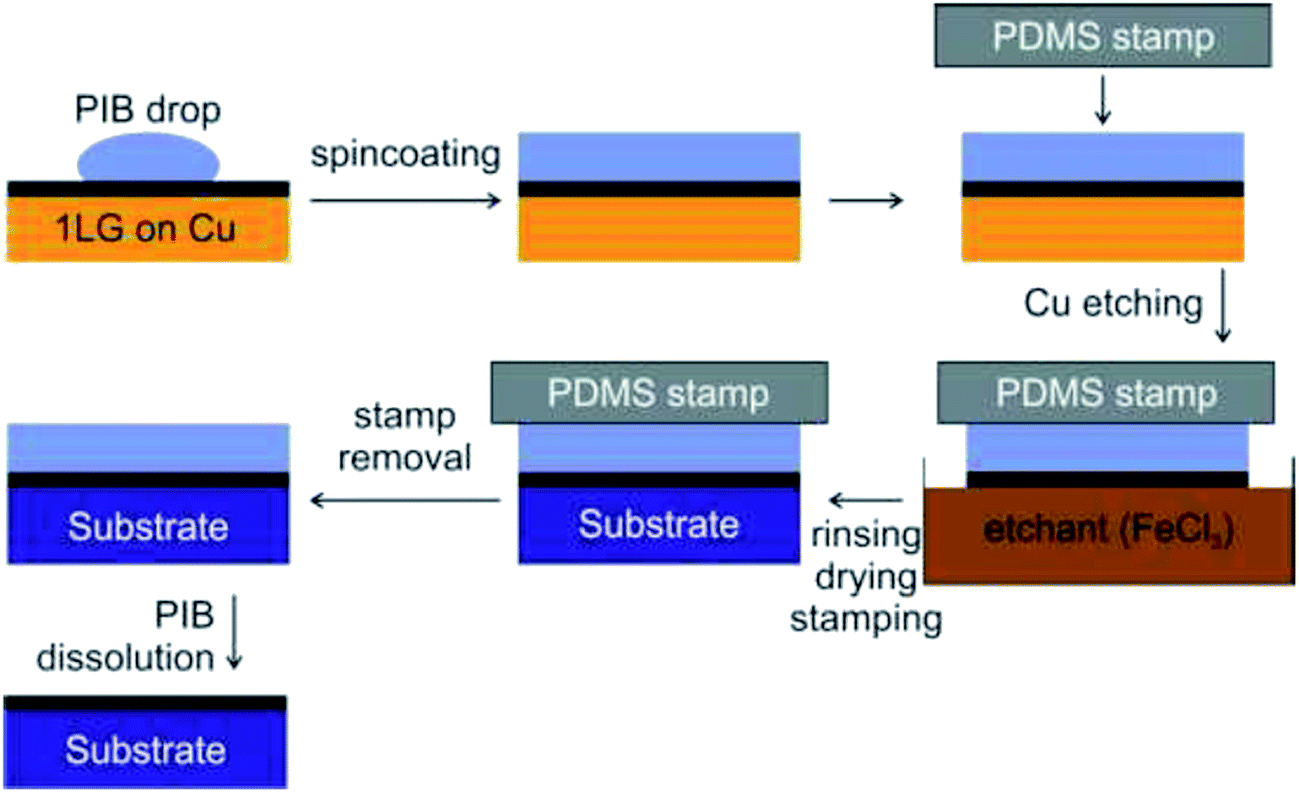 | ||
| Fig. 28 Schematic of the PIB-assisted transfer procedure. This figure has been adapted/reproduced from ref. 127 with permission from TANGER. | ||
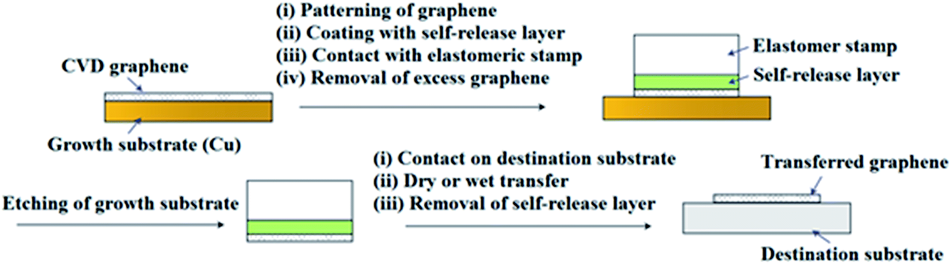 | ||
| Fig. 29 Schematic of the self-release layer (SRL) methodology in combination with a pick-and-place elastomer stamp. This figure has been adapted/reproduced from ref. 128 with permission from Nature Publishing Group. | ||
Besides, Chen et al.129 presented an economical and straightforward method to synthesize a graphene-based transparent conductive flexible substrate. This method made use of a photolaminator and commercial laminating film, which was made up of ethylene vinyl acetate (EVA) and polyethylene terephthalate (PET), to facilitate the graphene transfer process, as shown in Fig. 30. EVA film was attached to the FLG/Ni foil after it was heated using the photolaminator. A transparent conductive soft FLG/EVA/PET substrate was acquired after the commercial laminating film was ripped open. This easy and economical graphene transfer technique can widely open up the prospect for graphene-based applications in an environmentally friendly way.
 | ||
| Fig. 30 Schematic of the transfer sample preparation. This figure has been adapted/reproduced from ref. 129 with permission from Elsevier. | ||
Furthermore, Mafra's group130 developed a facile direct transfer method to transfer graphene layer to a targeted substrate. Instead of using an intermediate transfer layer, such as PMMA or PDMS, this transfer technique combines hot lamination of the target substrate onto a flexible substrate, followed by electrochemical delamination (bubble transfer) of the graphene layer. The reuse of the copper substrate can decrease the synthesis cost and chemical waste.
Furthermore, a new technique called the ‘room temperature rubbing method’ using sand paper (Fig. 31) was demonstrated by Jiang et al.131 Several advantages were highlighted, such as the method is suitable for both rigid and flexible substrates, single- and few-layer graphene can be transferred to new substrates, the transfer time is 1 min, represents an eco-friendly transfer approach and it preserve the benefits of previous rubbing technique, including room temperature and a cheap fabrication price.
 | ||
| Fig. 31 Schematic of the production steps: (a) sandpaper-rubbing step. (b) Double-smoothing–rubbing step. (c) Repeated-production step. (d) Soft-contact-rubbing procedure during the repeated-production step. (e) Restorative-rubbing procedure during the repeated-production step. This figure has been adapted/reproduced from ref. 131 with permission from Nature Publishing Group. | ||
5 Characterization of graphene
5.1 Raman spectroscopy
Raman spectroscopy is viewed as one of the most important characterization tools in graphene research132 and it has been used as a non-destructive tool to characterize graphene film. Carbon allotropes possess unique Raman characteristic peaks at around 1350, 1580 and 2700 cm−1.95,133 These can help researchers to determine the layer number and the quality of the graphene layers synthesized. The G band represents the tangential stretching (E2g) mode of highly oriented pyrolytic graphite (HOPG), whereas the D band originates from the disorder in the sp2-hybridized carbon atoms and is characteristic of lattice distortions.134–136 The 2D band originates from the second order Raman scattering process.134–136 There are few reports demonstrating that graphene film synthesized using a chemical reduction path contains a higher density of defects as compared to graphene prepared by CVD and other methods.23,137Fig. 32(a) shows the typical Raman spectra of graphene and graphite, where the prominent features of graphene are the appearance of three significant peaks of D, G and 2D at 1350, 1580 and 2680 cm−1, respectively. By comparison, both graphene and graphite showed a distinct difference in intensities of their D, G and 2D peaks, as seen in Fig. 32(a). Besides, the quality of graphene can be evaluated by calculating the ratio of the intensity of 2D/G (I2D/IG) from the Raman spectrum. A large ratio of I2D/IG and a comparably minor amplitude of D peak implies that good-quality graphene has been synthesized.132,133 In Fig. 32(b), graphene produced by CVD shows a much higher ratio of I2D/IG as compared to mechanically exfoliated graphene. Therefore, CVD is the preferable choice to synthesize high-quality graphene. Moreover, the small bump of the D peak reveals that high-quality graphene layers were produced, as shown in Fig. 32(b).138 | ||
| Fig. 32 (a) Raman spectra of graphene and graphite. This figure has been adapted/reproduced from ref. 132 with permission from Springer. (b) Raman spectra of CVD graphene and mechanically exfoliated graphene. This figure has been adapted/reproduced from ref. 138 with permission from American Chemical Society. | ||
The number of graphene layers can be estimated, as demonstrated by Yoon et al.133Fig. 33 shows a comparison of the G, G* and 2D band intensities for different numbers of graphene layers. For the G band, it is clear to see that the band intensity increased with the increasing number of layers up to 7 layers only and then it decreased for thicker layer samples. Therefore, the difference in intensity of the G band provides some clue about the number of graphene layers.133 For the Raman G* band, it has a relatively smaller intensity as compared to the G and 2D bands. It can be observed that the position of the G* band is shifted slightly from 2455 to 2445 cm−1 with the increasing number of graphene layers. Besides, the G* band of monolayer graphene in Fig. 33(b) is sharper as compared to few-layer graphene films. In addition, the 2D band of graphene can be used to differentiate between mono-, and more than one graphene layers.133 In Fig. 33(c), the 2D band of monolayer graphene has a sharper and greater intensity peak as compared to the others. Furthermore, Ferrari and co-workers also successfully differentiated mono-, bi- and several layers (<5 layers) by using Raman spectroscopy.139
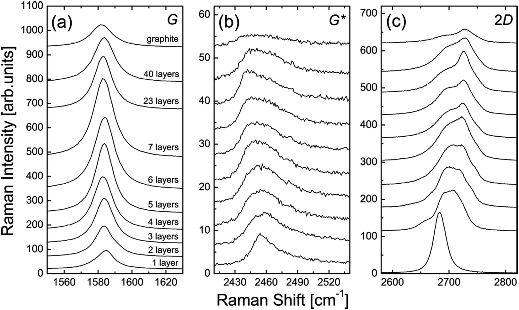 | ||
| Fig. 33 Evolution of the: (a) G band, (b) G* band, and (c) 2D band in the Raman spectra as functions of the number of graphene layers. This figure has been adapted/reproduced from ref. 133 with permission from Springer. | ||
5.2 FESEM and SEM
FESEM and SEM are widely used to investigate the morphological of graphene samples. An electron microscope has the same working principal as an optical light microscope, the only difference being that, instead of using visible light, highly energetic electrons are applied as the source in an electron microscope.140 Also, the optical light microscope has limitations on its resolution due to the wavelength of the visible light source, whereas the wavelength of accelerated electrons is much shorter to enable extremely high resolution in SEM and FESEM.141Xiu-Yun et al.142 obtained thin and flat graphene films, as shown in Fig. 34(a), by the centrifugation of expanded graphite. The expanded graphite was purified by using hydrogen peroxide without the use of sulfur, which is a novel method to prepare exfoliated graphite as the precursor for graphene synthesis. Fig. 34(b) and (c) depict graphene flakes that are transparent nanosheets, while Fig. 34(d) displays twisted and draped graphene films.
 | ||
| Fig. 34 FESEM images of thin graphene-like nanosheets in the upper liquid after centrifugation treatment. (a) Flat graphene film, (b and c) transparent graphene nanosheets, and (d) twisted and draped graphene. This figure has been adapted/reproduced from ref. 142 with permission from Springer. | ||
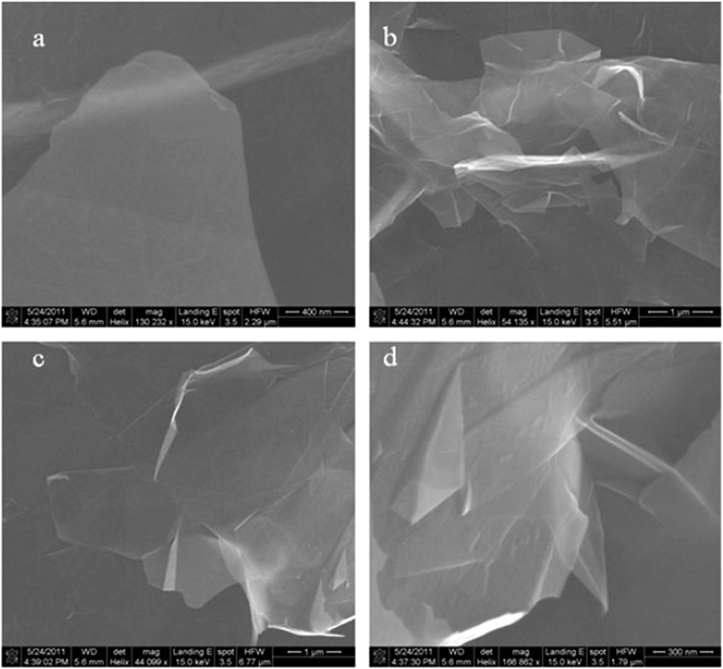
Fig. 35(a) and (b) show that few-layer graphene (FLG) comprise randomly individual graphene films, as synthesized by Khai and colleagues using a microwave-assisted solvothermal method.143 The dimensions of the graphene sheets was in the range of 3 to 10 μm. In Fig. 35(c) and (d), monolayer graphene sheets can be clearly seen at moderate and high magnifications of the FESEM images, respectively. In addition, crumples on the surface of the graphene film and folding at the corners can be observed clearly. On the other hand, in the few-layer graphene films also obtained by Gui's group144 using a solvothermal route, wrinkles and agglomerations could be seen, which agreed with the work done by Khai et al.143 The presence of residual oxygen-containing functional groups, including carboxyl groups (–COOH) and hydroxyl groups (–OH), attached on the sides of the graphene sheets might be the reason for the existence of wrinkles.143
 | ||
| Fig. 35 (a) Low-magnification, (b and c) moderate-magnification, (d) high-magnification FESEM images of few-layer graphene. This figure has been adapted/reproduced from ref. 143 with permission from Elsevier. | ||
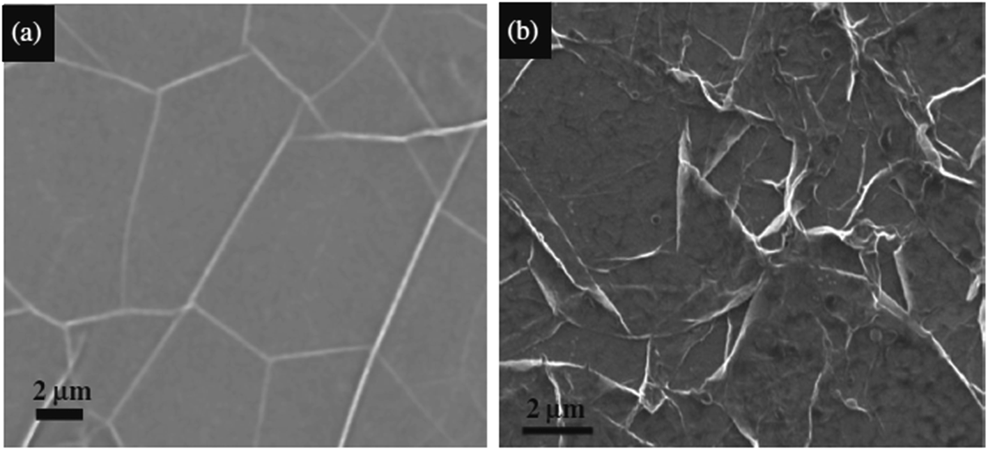
Hawaldar et al.145 observed a graphene sheet synthesized using hot filament thermal CVD (HFTCVD) on a copper substrate using FESEM, as shown in Fig. 36(a). Some wrinkles on the surface of the graphene films formed on the copper substrate could be observed. Fig. 36(b) displays a high-magnification FESEM image of the transferred bilayer graphene sheets on a copper TEM grid. In another synthesis of graphene sheets by CVD technique, Dang and co-workers146 discovered that the surface area of graphene nanoflakes increased with an increase in the graphene growth time. This can be seen from comparison of the graphene nanoflakes with growth times of 10 and 15 min, as shown in Fig. 36(c) and (d), respectively.
 | ||
| Fig. 36 (a) FESEM image of the as-grown graphene films on copper, (b) high-magnification FESEM image of a bilayer graphene sheet on a copper grid, prepared by hot filament thermal chemical vapour deposition. This figure has been adapted/reproduced from ref. 145 with permission from Nature Publishing Group, FESEM images of samples with graphene growth times of (c) 10 min and (d) 15 min. This figure has been adapted/reproduced from ref. 146 with permission from Elsevier. | ||
Fig. 37 shows the graphene film prepared by microwave plasma CVD (MPCVD), labelled G1, and the chemically prepared graphene, labelled G2.147 The graphene film produced by MPCVD on the polished surface consisted of some wrinkles on most of the sample surface, whereas the graphene film on the textured surface appeared to be deposited well on the surface. On the other hand, the chemically reduced graphene films were deposited non-uniformly and thus, agglomeration on the polished and textured surface was seen. FESEM can produce clear and less electrostatically distorted images with high resolution. It is also an effective tool to study the surface morphology of graphene samples.
 | ||
| Fig. 37 FESEM images of graphene film transferred onto: (a) polished Si and (b) textured Si substrates and chemically prepared graphene film spin-coated on: (c) polished Si and (d) textured Si substrates. This figure has been adapted/reproduced from ref. 147 with permission from Institute of Physics Publishing. | ||
In addition, SEM characterization is also very popular in graphene research because of its cheaper price than FESEM and its ability to scan the images at moderate magnification. Tu et al.148 demonstrated a CVD-synthesized graphene film on a Cu substrate and transferred the graphene film onto a Si substrate, as shown in Fig. 38. Mostly continuous graphene was seen despite there being a few white areas of wrinkles on the surface, as observed in the SEM images.
 | ||
| Fig. 38 (a) SEM image of a graphene sheet of 7 layers on a copper substrate. (b) SEM image of the graphene sheet of 7 layers transferred on a Si substrate, showing several wrinkles. This figure has been adapted/reproduced from ref. 148 with permission from Elsevier. | ||
Nicola and co-workers67 synthesized graphene film on a copper surface by using ethanol as the carbon feedstock via the CVD process. The influence of the growth parameters, i.e. reaction temperature and the growth time, were investigated on the synthesized graphene film. Fig. 39 displays the SEM images of the graphene film grown on the Cu substrate by varying growth times of 60 and 20 s, where a continuous graphene film covered the Cu substrate. High densities of wrinkles were formed during cooling due to the difference in thermal expansion between the produced graphene film and the copper substrate. Darker islands aligned in the direction of the lamination of the copper foils can be seen in the graphene film, which indicate that the secondary nucleation was started in a short growth time.
 | ||
| Fig. 39 SEM images of graphene grown on copper at 1070 °C with 100 sccm H2: (a) growth for 60 s, (b) and (c) growth for 20 s. The dashed lines show the copper grain edges and boundaries. This figure has been adapted/reproduced from ref. 67 with permission from Elsevier. | ||
Besides, SEM was employed to monitor the in situ graphene growth in a carbon segregation process, as demonstrated by Takahashi and colleagues.149 Several numbers of graphene layers were synthesized using different growth conditions, as shown in Fig. 40(a), in which thicker graphene layers are seen as darker at the right-hand side of the image. In contrast, bilayer graphene shows an intermediate contrast, whereas monolayer graphene film appeared as a slightly brighter contrast on the Ni surface. The change of contrast, as seen in the SEM images, was due to the change in the work function, which was 5.3 eV for the Ni(111) surface, 3.9 eV for the single-layer graphene-covered surface and 4.6 eV for the graphite surface, and also due to the different numbers of valence electrons between Ni and graphite.150 When the sample was cooled to room temperature in vacuum, the difference in contrast was improved (Fig. 40(b)). After air exposure of the graphene sample, the colour contrast of the graphene layer changed significantly due to the oxidation of the Ni surface, as displayed in Fig. 40(c). However, the area covered by the graphene layer was protected from oxidation.151
 | ||
| Fig. 40 SEM images showing the contrast for different numbers of layers of graphene on polycrystalline nickel observed at: (a) an elevated temperature during carbon segregation, (b) room temperature without exposure to air, and (c) room temperature after exposure to air. This figure has been adapted/reproduced from ref. 149 with permission from Elsevier. | ||
In addition, Fig. 41 shows the graphene film synthesized on the surface of an iridium (Ir) substrate by using ethylene as a carbon precursor via CVD.152Fig. 41(a) displays the results from when a relatively low dose of 10.8 L at 800 °C was used, in which it can be seen that many dark circular graphene islands with uniform diameters are formed. However, the continuous flat film was observed when a higher ethylene dose of 18 L was used. The absence of colour contrast in Fig. 41(b) indicates that a coherent graphene layer covered 100% of the Ir substrate surface. In another investigation on the effect of the amount of CH4, a low CH4 concentration produced a 70% area coverage of the Cu substrate surface by graphene, compared to full area coverage under high CH4 concentration conditions, as shown in Fig. 42(a) and (b).153Fig. 42(c) and (d) show multilayer graphene domains with a mean size of 4 μm and 2 μm, respectively.
 | ||
| Fig. 41 (a) SEM image (12 μm × 9 μm) and (b) SEM image (12 μm × 9 μm) of a fully graphene-covered surface, showing a coherent graphene layer. This figure has been adapted/reproduced from ref. 152 with permission from Elsevier. | ||
 | ||
| Fig. 42 SEM images of CVD graphene on Cu: (a) 5 ppm CH4 for 60 min, (b) 10 ppm CH4 for 60 min, (c) 20 ppm CH4 for 30 min, (d) 30 ppm CH4 for 20 min. Some are highlighted by dashed blue circles in images (c) and (d) and represent multilayer graphene domains. This figure has been adapted/reproduced from ref. 153 with permission from Institute of Physics Publishing. | ||
5.3 TEM
TEM utilizes very high voltage electrons to transmit through a thin sample and then the signal received is processed for projection onto a viewing screen for observation.154 Therefore, a thin sample is preferable for TEM analysis. TEM characterization is very important in graphene research due to its ability to image graphene at the atomic level;155 for instance, for point defects, Stone–Wales rotation, vacancy, dislocations and many more.156Monolayer graphene can be regarded as a transparent sheet using TEM characterization. The low- and high-magnification TEM images of a monolayer graphene film transferred onto a TEM grid are shown in Fig. 43(a) and (b), respectively, together with the corresponding selected area electron diffraction (SAED) pattern (inset).148 Monolayer graphene can be identified from the TEM image, as displayed in Fig. 43(b), whereas the SAED pattern (inset in Fig. 43(b)) reveals the typical hexagonal crystalline nature of graphene. In addition, 2–7 graphene layers can be clearly seen in the TEM micrographs in Fig. 44(a)–(f). The SAED patterns shown in Fig. 44(g)–(i) are irregular, and the bilayer graphene, trilayer graphene and five-layer graphene films cannot be justified based on these patterns. Thus, other characterizations, such as Raman spectroscopy, are crucial to support the TEM results.
 | ||
| Fig. 43 (a) Low- and (b) high-magnification TEM images of monolayer graphene, where a SAED pattern recorded from the centre of the domains is shown in the inset. This figure has been adapted/reproduced from ref. 148 with permission from Elsevier. | ||
 | ||
| Fig. 44 High-resolution TEM images of the edges of graphene with different numbers of layers: (a) bilayer, (b) trilayer, (c) four layers, (d) five layers, (e) six layers and (f) seven layers. The typical SAED images of bilayer, trilayer and five-layer graphene taken from the centre of the domains are shown in (g)–(i), respectively. This figure has been adapted/reproduced from ref. 148 with permission from Elsevier. | ||
Fig. 45(a) shows the TEM micrographs of graphene growth by using ethanol as a carbon precursor via the CVD process. The produced graphene film was well formed and continuous on the microscopic scale. Fig. 45(b) and (d) display the folded edges of the graphene films (monolayer and bilayer graphene, respectively), which enable the number of layers of the graphene membrane to be estimated. Besides, the SAED analysis in the inset images shows that the graphene sheets produced were polycrystalline.67
 | ||
| Fig. 45 TEM characterization of graphene films transferred onto TEM grids (a) image of a graphene film grown for 20 s at 1000 °C and inset of the electron diffraction pattern of the area, showing a polycrystalline graphene film. (b) High-resolution image of a monolayer graphene fold. (c) Micrograph of a film grown for 1 min at 1070 °C and inset of the electron diffraction pattern of the area. (d) High-resolution image of a bilayer graphene fold. This figure has been adapted/reproduced from ref. 67 with permission from Elsevier. | ||
Single-layer graphene sheets can also be synthesized by using zeolite Ni-MCM-22 as both the template and catalyst. Fig. 46 shows the TEM image of the agglomerated graphene sheet, while the inset image shows the single-layer graphene. It can be seen under TEM observation that the graphene materials are transparent and interlaced nanosheets. Furthermore, it was proven that the synthesized nanosheets of the graphene materials were flat and ultrathin.80
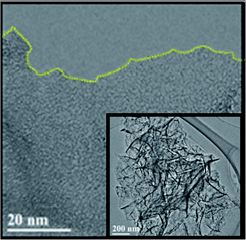 | ||
| Fig. 46 TEM image of the agglomerated graphene. The inset indicates the single-layered graphene. This figure has been adapted/reproduced from ref. 80 with permission from Elsevier. | ||
To analyse the crystallinity of the graphene territories, selected area electron diffraction (SAED) patterns were identified from six different areas (1–6) of the graphene region in Fig. 47(a). Fig. 47(b) shows a cracked site of the graphene region. Fig. 47(c) displays the existence of single-layer graphene. As seen in Fig. 47(d), all the scanned six regions were identified as single-crystalline graphene due to there being only one set of hexagonal diffraction spots without rotation shown. Therefore, the whole graphene region as marked by 1–6 in Fig. 47(a) comprises a single crystalline film.157
 | ||
| Fig. 47 (a) Low-magnification TEM image of a corner in a square graphene domain transferred to TEM grids. (b) TEM image of a cracked area on the graphene domain. (c) High-resolution TEM image taken from the region marked with the arrow in (b). (d) SAED of the six areas numbered in (a). This figure has been adapted/reproduced from ref. 157 with permission from American Chemical Society. | ||
5.4 UV-vis spectroscopy
UV-vis spectroscopy measures the absorption and reflectance of radiation in the UV spectral range. The atoms or molecules in the tested material absorb light in the visible, near UV and infrared regions through the electronic transitions. When the attenuation of the beam is increased, the absorbance of the sample solution will also be increased. The absorbance depends on the concentration of the solution, as stated by Beer's law.158–160 Normally, UV-vis is used to characterize the optical transparency of graphene film by measuring the transmittance or absorbance characteristics of a sample.161 An absorption or transmittance spectrum displays a number of absorption or transmittance bands corresponding to the transition of an electron from the lowest energy state to the excited state.162 Therefore, the UV-vis spectrum could be used to investigate the properties of produced graphene layers.159UV-vis characterization can be performed to confirm that GO has reduced to reduced graphene oxide (RGO) successfully, where the attached oxygen-based functional groups at the basal plane surfaces and edges of GO are removed to obtain the RGO.163 Typically, GO has an absorption spectrum peak at 230 nm, which is attributed to π–π* transition caused by the aromatic ring (C–C), whereas RGO shows a peak that is red-shifted to 270 nm because of n–π* transition by the carbonyl bonds (C![[double bond, length as m-dash]](https://www.rsc.org/images/entities/char_e001.gif) O).164,165Fig. 48 shows the absorbance of RGO synthesized at different reaction times. It can be clearly seen that the absorption spectrum peak of RGO that appeared at 231 nm is gradually red-shifted to 270 nm with the increasing reaction time. When the absorption peak was shifted to more than 270 nm, this indicates the completion of the reduction of GO to RGO. It also shows that the synthesis of RGO is chemically controllable for modification of its optical and electrical properties.166
O).164,165Fig. 48 shows the absorbance of RGO synthesized at different reaction times. It can be clearly seen that the absorption spectrum peak of RGO that appeared at 231 nm is gradually red-shifted to 270 nm with the increasing reaction time. When the absorption peak was shifted to more than 270 nm, this indicates the completion of the reduction of GO to RGO. It also shows that the synthesis of RGO is chemically controllable for modification of its optical and electrical properties.166
 | ||
| Fig. 48 UV-vis absorption spectra showing the change of GO as a function of reaction time. This figure has been adapted/reproduced from ref. 166 with permission from Nature Publishing Group. | ||
In addition, UV-vis spectroscopy could be used to assist in verifying the number of graphene layers. Fig. 49(a) illustrates the different spectra for the optical transmittance of 1 to 5 graphene layers.167 The increasing number of graphene layers reduces the optical transmittance. In particular, a lesser quantity of light can transmit through a thicker graphene film. In Fig. 49(a), the green spectrum relates to the transmittance of bare quartz where the graphene film was deposited for the measurement. The transmission of all the samples decreased from a wavelength of 250 to 300 nm and then became linear from 600 to 1000 nm.167 In addition, investigation of monolayer graphene was also reported by Ago et al.168 The approximation of the layer number of a graphene sample according to the I2D/IG ratio and the broadness of the 2D band from Raman spectrum is not sufficient or precise as unexpected doping might have occurred in the graphene sample in the middle of the growth and transfer operations. This unintentional doping of graphene can alter the I2D/IG ratio and lead to the wrong information being obtained about the quality of the graphene film. Moreover, the 2D band of bilayer graphene can have a relatively narrow line width of 30–40 cm−1, which is very small to be observed and can mislead the estimation of the number of graphene layers. Hence, Hiroki and co-workers utilized UV-vis spectroscopy to verify that the transferred graphene film was single-layer graphene by measuring the light transmittance. The results showed that the optical transmittance was ca. 2.2% at 550 nm, which is commensurate with the hypothetical value of monolayer graphene, i.e. 2.3%. Therefore, the transferred layer could be verified as single-layer graphene by the supporting optical transmittance from the UV-vis spectroscopy analysis. Furthermore, Fig. 49(b) displays a similar optical transmittance value of the monolayer by S. Bae et al. as well.100 Further increases in the number of graphene layers reduces the optical transmittance by approximately 2.2–2.3% per layer, which is in agreement with the aforementioned optical transmittance value.
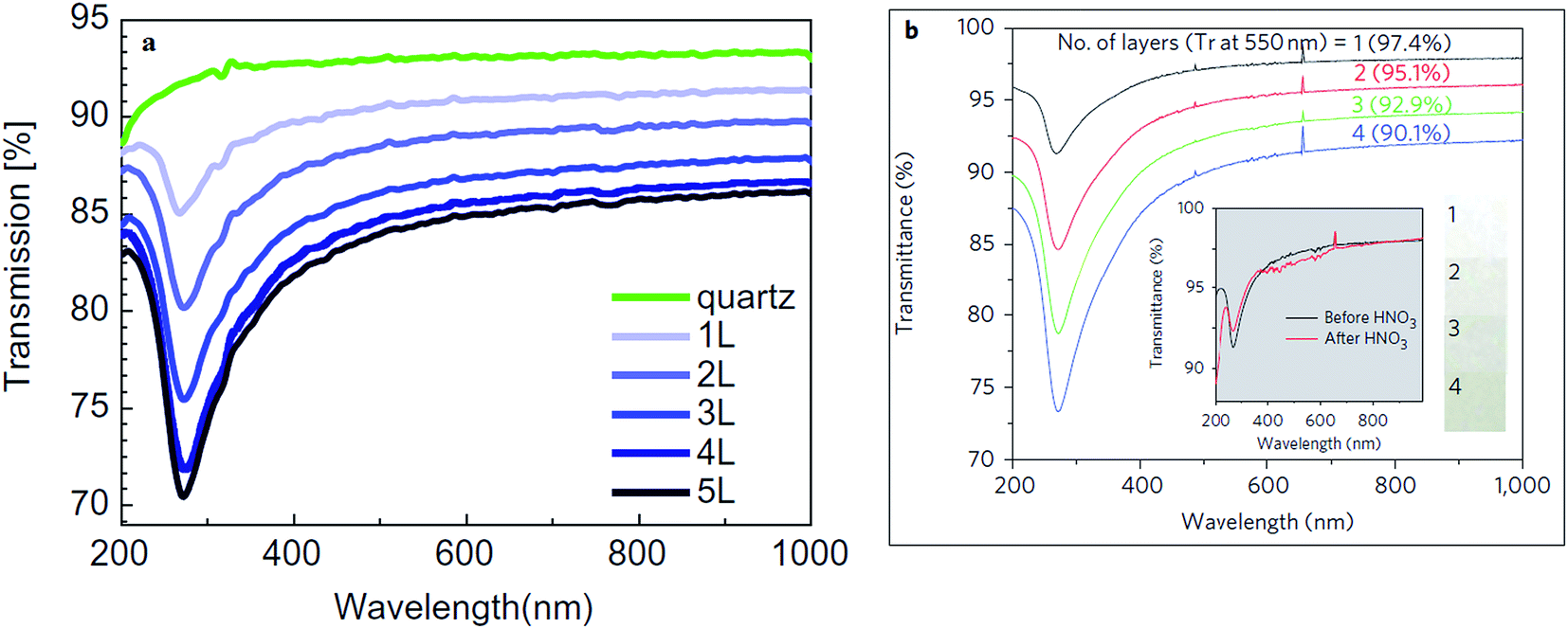 | ||
| Fig. 49 (a) UV-vis optical transmittance for bare quartz and for different layers of graphene films on quartz. This figure has been adapted/reproduced from ref. 167 with permission from Elsevier, (b) UV-vis spectra of transferred graphene films on quartz substrates. This figure has been adapted/reproduced from ref. 100 with permission from Nature Publishing Group. | ||
In addition, graphene film is very useful in solar cells and optoelectronics applications because of its excellent optical transmittance and electrical conductivity, which make it a promising successor to substitute the currently used materials, i.e. indium tin oxide (ITO) and fluorine tin oxide (FTO). Moreover, Dodoo-Arhin et al.169 demonstrated the excellent properties of graphene by investigating and comparing the optical transmittance of graphene film and of a conventional transparent electrode, ITO. Graphene had a higher optical transmittance of 97.7% compared to ITO with a value of 90.5% as well as a lower sheet resistance than ITO film. Thus, graphene can allow light to pass through, while simultaneously possessing a better electrical conductivity. These unique properties are particularly essential in photovoltaic applications.
5.5 XRD
XRD, also called ‘X-ray crystallography’, can be used to study the crystallinity, atomic arrangement, crystallite size, imperfections and other aspects of a material's structure. A crystalline material in its crystal lattice is classified by its orderly, continuously repetitive arrangements of planes of atoms.170 X-rays from an XRD instrument are transmitted, absorbed, refracted, scattered and diffracted.171 A unique diffraction spectrum is produced when X-rays from an XRD instrument are emitted on a crystalline material.172 Furthermore, the separation of the planes of atoms in a material can be calculated according to Bragg's law.170 Similar substances produce similar XRD spectra, hence a unique XRD pattern can be viewed as the fingerprint reference to identify a substance.173 Each substance in a mixture of substances gives individual diffraction patterns independently of the other components. For the characterization of graphene, although XRD can be utilized as a characterization tool, it is not an ideal tool to define monolayer graphene. Nevertheless, XRD characterization is helpful in determining monolayer graphene.Naebe et al.174 functionalized and characterized thermally reduced graphene nanoplatelets, which have significantly improved thermal stability and mechanical properties compared to GO. The XRD results displayed graphite, GO, thermally reduced graphene (TRG) and functionalized graphene (FG), as shown in Fig. 50(a). A sharp diffraction peak at 2θ = 26.5° illustrated by pristine graphite is commensurate with the plane (002) well-ordered carbon atoms with an interlayer spacing of 3.35 Å. However, the well-ordered graphite peak at 26.5° disappeared, while a lower peak was seen at 2θ = 10.5°, which signifies the diffraction of the (002) GO plane with a calculated interlayer spacing of 8.41 Å. This implies that large amounts of oxygen atoms are incorporated at the GO surface and thus, the GO interlayer spacing is expanded. The elimination of oxygen functional groups in GO in the high-temperature process resulted the disappearance of the (002) peak and the formation of thermally reduced graphene sheets. Wang and co-workers175 also reported that the 2–5 reduced graphene layers had no (002) peak after microwave irradiation treatment or other distinct peaks, as seen in Fig. 50(b).
 | ||
| Fig. 50 (a) XRD plots for graphite, GO, graphene and FG. This figure has been adapted/reproduced from ref. 174 with permission from Nature Publishing Group, (b) XRD patterns of natural graphite, GO and graphene. This figure has been adapted/reproduced from ref. 175 with permission from The Science Press. | ||
5.6 AFM
AFM can be utilized for the characterization of samples with dimensions in the nanometre range in different conditions, i.e. normal atmosphere, liquids and ultrahigh vacuum.176 A nanometre-sharp AFM tip made by micro-fabricating technology is attached to the free edge of an adjustable cantilever, which is the transducer to sense the tip on the sample.177You et al.178 measured the thickness and the surface roughness of graphene film using AFM for gas sensor applications to determine the best growth condition. Fig. 51 shows the graphene films produced on four different substrates that were characterized by AFM tapping mode. It was found that among all the samples, a longer CVD reaction time increased the surface roughness and the thickness of the graphene layer due to more graphene layers being formed.
 | ||
| Fig. 51 The images of SA1, SA2, SA3 and SA4 obtained in the close contact mode. Size: 3 μm × 3 μm. This figure has been adapted/reproduced from ref. 178 with permission from American Society for Engineering Education. | ||
Gao et al. performed graphene synthesis on a palladium (Pd) substrate by a surface segregation technique,85 with Fig. 52 displaying the AFM images indicating the film thickness and surface morphology of the graphene layer on Pd substrate surface. It can be seen that a uniform graphene film enclosed the Pd substrate completely, as illustrated in Fig. 52(a) and (b). Nonetheless, it was also observed that there were some carbon nanowires present on top of the graphene layer because of 3D carbon growth. The border of the sample shows the discontinuity of graphene, where a graphene area and uncovered Pd(111) surface can be seen in Fig. 52(c). The thickness of the line profile from Fig. 52(c) was measured to be approximately 0.40 nm, which is in agreement with the theoretical thickness of a monolayer graphene.
 | ||
| Fig. 52 AFM topography images of graphene grown on Pd(111) surfaces. Images (a and b) were taken from the centre of the sample, where the surfaces were covered by a uniform graphene layer except for some carbon nanowires formed on top of the graphene layer. Image (c) was taken from the edge of the sample, which shows the graphene region and bare Pd(111) surface. Image (d) shows the height of the graphene layer corresponding to single-layer graphene. This figure has been adapted/reproduced from ref. 85 with permission from Elsevier. | ||
AFM represents an effective technique to justify the thickness of graphene layer. Liu's group90 produced few-layer graphene by exfoliating expandable graphite in supercritical N,N-dimethylformamide (DMF) solvent. Fig. 53(a) and (b) show the graphene layers imaged by AFM tapping mode and the line profiles in the AFM images. It can be observed from the AFM images that the sizes and thicknesses vary, whereas most of the areas of all the synthesized few-layers graphene sheets were around 3 nm. On the other hand, Fig. 53(c) and (d) illustrate the AFM topography photographs of the exfoliated few-layers graphene. The height of the exfoliated few-layers graphene sheet is about 1.2 nm, which suggests it should be considered as single-layer graphene.
 | ||
| Fig. 53 Typical tapping mode AFM images of (a) few-layer graphene sheets 2 μm × 2 μm, (b) few-layer graphene sheets 0.8 μm × 0.8 μm, (c) monolayer graphene sheets 3 μm × 3 μm, and (d) monolayer graphene sheets 1.25 μm × 1.25 μm deposited on the mica substrate from dispersion, corresponding height cross-sectional profile. This figure has been adapted/reproduced from ref. 90 with permission from Elsevier. | ||
6 Growth mechanism of single-layer graphene
6.1 Differences between segregation–precipitation and surface adsorption
For the huge-scale production of monolayer and few-layers graphene films, CVD has been the most common choice to date. The growth mechanism of graphene film relies upon the types of metal catalyst utilized for growing the graphene layer. Two types of graphene growth mechanisms via CVD, namely surface adsorption and segregation followed by a precipitation process, have been proposed in the literature recently.21,179Fig. 54 illustrates the common flow to obtain a graphene layer by the segregation/precipitation process and by the surface adsorption process via CVD.180 The segregation and precipitation process happens when carbon atoms diffuse into the metal catalyst at high temperature, and consequently, the diffused carbon atoms segregate onto the metal catalyst surface used and precipitate during the cooling period.14,181 The segregation process begins when the quantity of carbon atoms in the bulk metal is sufficiently high or in the middle of the cooling step, and eventually the carbon species are arranged in such a way that the hexagon structure of a graphene basic unit is organized to form a graphene layer.21 However, surface adsorption occurs when the hydrocarbon dissociates and the carbon atoms stay on the metal substrate surface without segregating and precipitating. The precipitation and segregation graphene growth mechanism occurs with metal substrates with great carbon solubility, which allows the carbon species to diffuse and disperse into the metal catalyst substrate.21,182 On the other hand, surface adsorption typically occurs in metal substrates with low carbon solubility, such as copper.21 | ||
| Fig. 54 Sketch of graphene formation by both direct chemisorption/deposition on Cu and by precipitation/segregation on Ni. This figure has been adapted/reproduced from ref. 180 with permission from The Royal Society of Chemistry. | ||
6.2 Nickel substrate
Nickel (Ni) is one of the most common transition metal substrates utilized to grow carbon nanomaterials. The formation of graphene films on Ni surface by the segregation and precipitation process takes place due to the high carbon solubility in Ni. The reported carbon solubility of Ni film of approximately 700 nm thickness is 0.9% and 1.15% at 900 °C (ref. 182) and 1000 °C,183,184 respectively. Before the segregation and precipitation processes occur, carbon species dissociate from the hydrocarbons and diffuse into the bulk Ni substrate. Subsequently, the formation of a graphene layer on the Ni substrate surface occurs during the cooling step by segregation of the saturated carbon atoms, immediately followed by precipitation of the carbon atoms. This precipitation process results in the formation of a graphite layer, which causes high carbon solubility metal inappropriate to achieve monolayer graphene.182 Recently, Momiuchi's group185 observed the dissolved carbon atoms segregate onto the flat polycrystalline substrate surface from the bulk Ni substrate during the segregation process by utilizing in situ SEM. The nucleation sites are favourable to occur on large Ni(111)-oriented grains and they possess step-bunched structures.185In addition, Li et al.182 employed mixed carbon isotopes labelling to show that the segregation and precipitation of carbon would occur on a Ni substrate after the dissolution of carbon isotopes. The schematic diagram, as shown in Fig. 55, distinctly displays that a uniform mixture of carbon isotopes was obtained after consecutive isotopic carbons were introduced. Thus, a graphite layer could be formed when too many carbon atoms are precipitated after the segregation of the first graphene layer.21,182,186 Therefore, it would be possible to synthesize monolayer graphene on a Ni substrate by suppressing the amount of carbon atoms available for precipitation in fast cooling after the CVD process. Umair and Raza187 found that an ultra-fast cooling method, involving a quenching technique, can obstruct the precipitation of extra carbon atoms onto the nickel surface and hence, can reduce the number of graphene films produced.188 Besides, an instant decrease in the sample temperature can inhibit the further segregation process of carbon atoms to form bilayer graphene.188
 | ||
| Fig. 55 Graphene with randomly mixed carbon isotopes arising from the segregation and precipitation process. This figure has been adapted/reproduced ref. 182 with permission from American Chemical Society. | ||
6.3 Nickel/molybdenum substrate
In a recent study, Lee et al.179 compared the graphene growth mechanism using a few types of metal catalyst substrates, namely pure nickel metal films, nickel sheets deposited on molybdenum (Ni/Mo) and platinum sheets. In agreement with the findings of Ahmad et al., Lee and co-workers concluded that the precipitation and segregation of carbon atoms do happen in the graphene synthesis using Ni substrates. Moreover, under an exceedingly low methane gas flow rate and reaction time, carbon atoms preferably precipitate along the Ni grain boundary rather than via surface diffusion, thus resulting in a partial growth of graphene. Fig. 56 shows the optical images of the partial synthesis of a graphene layer on Ni/SiO2/Si substrates under a short growth duration of 30 s, a low CH4 flow rate of 2 sccm and a rapid cooling process (8 °C s−1). The grain boundaries of the Ni substrate and monolayer graphene on the Ni films can be clearly seen in Fig. 56(b) and (c), respectively, which agree with the Raman results. Besides that, when the cooling process of the Ni substrate was prolonged to induce a sufficient diffusion of carbon atoms, few-layered graphene structures were detected at the Ni grain boundaries.179 This is in agreement with previous research stating that the grain boundaries tend to facilitate the paired processes of the segregation and precipitation of carbon species on a Ni surface and the subsequent formation of multilayer graphene.189 Besides, it was discovered that monolayer and bilayer graphene are more preferably formed on a single-crystal Ni surface than on polycrystalline Ni because of the absence of grain boundaries.179 | ||
| Fig. 56 (a) Low-magnification optical microscope image of as-synthesized graphene on Ni/SiO2/Si substrate using 2 sccm CH4, 30 s growth duration and a fast cooling process. (b) & (c) High-magnification images of the regions corresponding to the region in (a). Dashed circle in (a) presents a boundary where graphene is synthesized. This figure has been adapted/reproduced from ref. 179 with permission from Springer. | ||
In addition, Lee and colleagues179 also reported that when Ni/Mo substrates were used, the dominant graphene growth mechanism was adsorption driven. The dissolved carbon atoms formed molybdenum carbide, Mo2C, to prevent the huge amount of carbon diffusion to the Ni/Mo surface. The results demonstrated that monolayer graphene films can be obtained relatively easy over a broad range of growth conditions by suppressing the carbon precipitation from the bulk to the surface via the formation of Mo2C. The AFM results in Fig. 57 show a smooth surface and a lack of multilayer graphene along the grain boundaries, which indicates there was no preferential precipitation of carbon at the grain boundaries. In addition, Dai et al.190 also demonstrated that Ni/Mo suppressed the carbon precipitation process by establishing a firm metal carbide and inducing the formation of monolayer graphene. Besides the Ni/Mo alloy, other alloys, such as cobalt–molybdenum (Co–Mo), which contains an active catalyst component, can strictly produce single-layer graphene film, as reported in the same study.
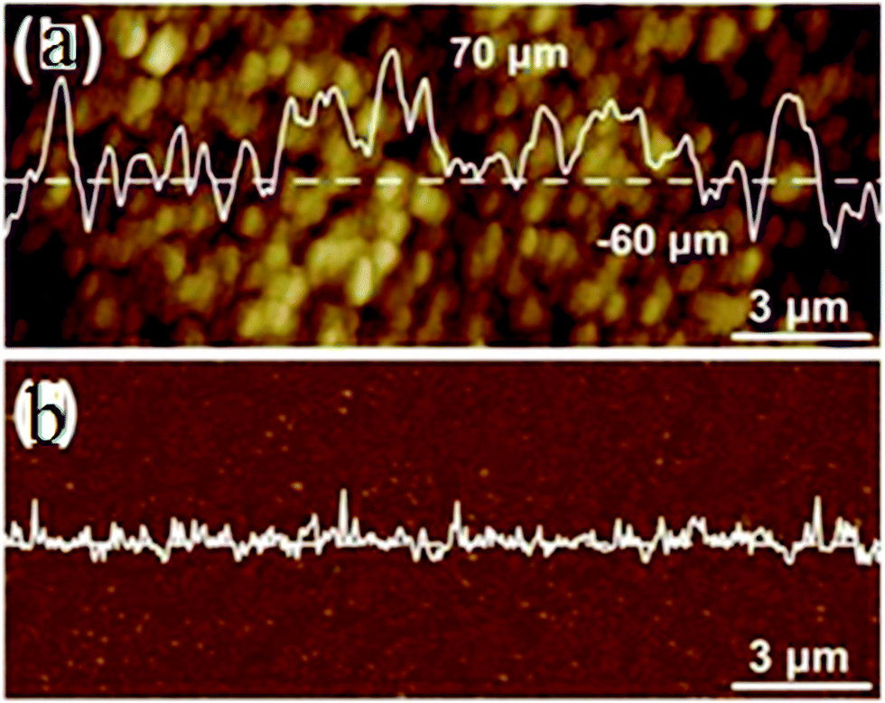 | ||
| Fig. 57 (a) AFM image of Ni/Mo substrate after annealing at 1000 °C, (b) AFM image of graphene transferred onto SiO2/Si substrate. Insets are line profiles at the dashed line. This figure has been adapted/reproduced from ref. 179 with permission from Springer. | ||
6.4 Platinum substrate
Graphene film is believed to be grown on a platinum (Pt) substrate by a precipitation and segregation process115,191,192 due to the great carbon solubility of 0.9 at% in the Pt substrate at 1000 °C,193 which is slightly below the carbon solubility of Ni (1.15 at%). In contrast, Lee et al.179 discovered that graphene film was formed on a Pt substrate by an adsorption process, then followed by a carbon precipitation mechanism. The OM and AFM results reveal obvious grain boundaries and a huge grain size on the Pt sheets, as shown in Fig. 58. It was mentioned previously in the past study189 that multilayer graphene films are expected to grow on Pt along the grain boundaries if the dominant growth mechanism on Pt is a precipitation-related processes. However, the synthesized monolayer graphene film was smooth and had an absence of multilayer graphene sheets. Hence, Lee's group concluded that surface adsorption is more dominant in graphene synthesis on a Pt substrate. Besides, Lee et al.179 also demonstrated that the precipitation of the remaining carbon from the previous growth led to the formation of graphitic flakes after continuous thermal annealing of the Pt substrate. The graphical illustration in Fig. 59 shows the step flow of the graphene layer formation and graphitic flakes via carbon precipitation mechanism on Pt substrate. | ||
| Fig. 58 (a) Optical microscopy and (b) AFM images of Pt sheet obtained after annealing at 1000 °C. This figure has been adapted/reproduced from ref. 179 with permission from Springer. | ||
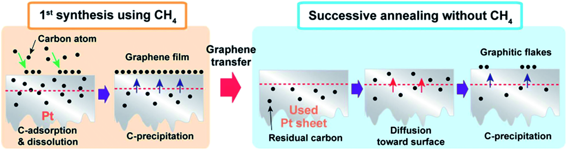 | ||
| Fig. 59 Schematic of the formation of graphene and graphitic flakes by a carbon precipitation mechanism in Pt. This figure has been adapted/reproduced from ref. 179 with permission from Springer. | ||
Sun et al.194 discovered that a sequence of surface catalysis and carbon segregation occur on a platinum (Pt) substrate in CVD. This catalysis process on the surface induces the self-limiting formation of single-layer graphene at high temperature, while the segregation process produces multilayer graphene at low temperature during the graphene synthesis process. Besides, Sun's group proposed the main processes that are taking place during graphene synthesis are graphene deposition, absorption and segregation, as depicted in Fig. 60. A graphene layer will be formed when the deposition rate is higher than the absorption rate. In addition, two different regimes were suggested, namely the balance regime and segregation regime. The balance regime refers to a kinetic balance dissolution, and the formation of graphene occurs when the deposition rate equals the absorption rate. On the other hand, in the segregation regime, the segregation rate is higher than the absorption rate that arises in the synthesis of multilayer graphene from underneath the existing formed graphene layer.
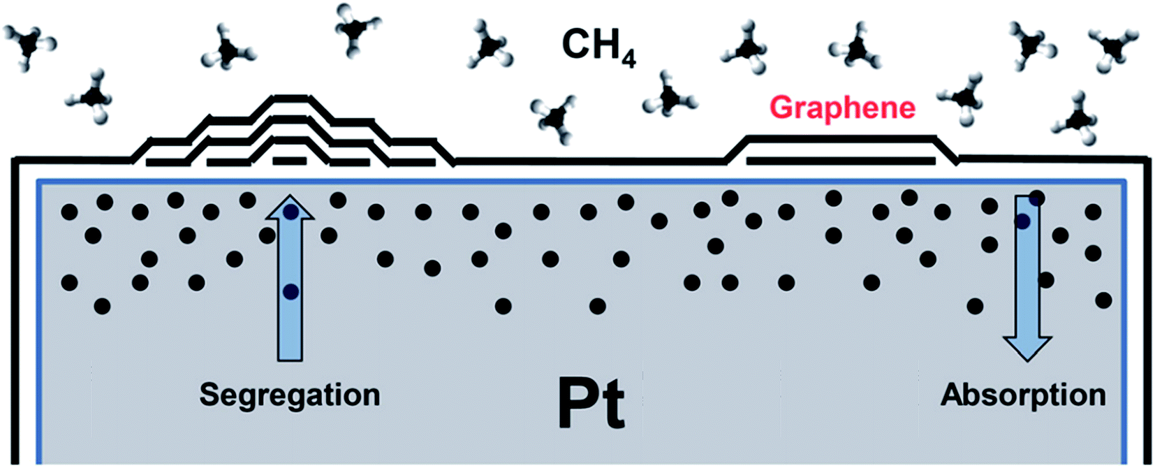 | ||
| Fig. 60 Schematic of the graphene growth mechanism over Pt surface. Two regimes (balance and segregation) can be defined by the relative strength of carbon deposition, absorption and segregation. This figure has been adapted/reproduced from ref. 194 with permission from American Institute of Physics Publishing. | ||
6.5 Copper substrate
Copper (Cu) is a common metal substrate, where the surface adsorption mechanism is dominant due to its low carbon solubility of 0.02 at% as reported.184,195 In contrast to the segregation and precipitation mechanisms that occur on Ni substrates, graphene is formed on a Cu substrate without the dissolution of carbon species into the bulk Cu substrate. Therefore, a high-quality and homogenous single-layer graphene film can form on a Cu catalyst substrate via this surface adsorption mechanism, as shown in Fig. 61.113,196 The formation of the first layer of graphene film covering the surface of the Cu substrate can inhibit the exposure of the catalyst to induce further dissociation of the hydrocarbon gas precursor plus the growth of graphene underneath the first layer graphene.196,197 Furthermore, this surface adsorption mechanism is self-limiting,196 which is evidenced by the carbon isotope labelling from the hydrocarbon precursors.182 Li et al. proposed a surface adsorption mechanism in the Cu substrate, as shown in the schematic diagram in Fig. 62. | ||
| Fig. 61 Schematic of graphene growth mechanism on Cu surface. This figure has been adapted/reproduced from ref. 196 with permission from American Chemical Society. | ||
 | ||
| Fig. 62 Graphene growth with separated isotopes by surface adsorption. This figure has been adapted/reproduced from ref. 182 with permission from American Chemical Society. | ||
7 Growth mechanism of multilayer graphene
Kalbac et al.198 proposed that the growth of graphene on a Cu substrate is initiated via the formation of a multilayer graphene cluster and removal of the upper layers by hydrogen etching. The growth of upper graphene layers is slower than the underneath layer due to the exposure of the upper layers to the hydrogen etching process. In addition, Liu et al.199 demonstrated the growth of a multilayer graphene film and large-dimension single-crystal single-layer graphene on a Cu substrate via the CVD method. A growth mechanism of multilayer graphene called the ‘on-top growth mechanism’, as shown in Fig. 63, was proposed by Liu and co-workers. The annealing step of the Cu foil at a high temperature can generate some Cu oxide nanoparticles, as depicted in Fig. 63(b). These Cu oxide nanoparticles work as nucleation sites for the graphene layer to grow and limit the density of the graphene domains in different concentrations of hydrogen. The uppermost graphene layer's growth speed is greatly influenced by the hydrogen concentration, which agrees well with Kalbac's group.198 When the hydrogen concentration is high, the growing speed of the bottom graphene layer nearest to the Cu catalyst surface is faster than the top layer graphene due to the hydrogen etching process and eventually single-crystal single-layer graphene can be produced. On the other hand, when the hydrogen concentration is low, the bottom and top graphene layers grow at a comparatively similar speed. Hence, the synthesis of better quality multilayer graphene was achieved using a low hydrogen concentration.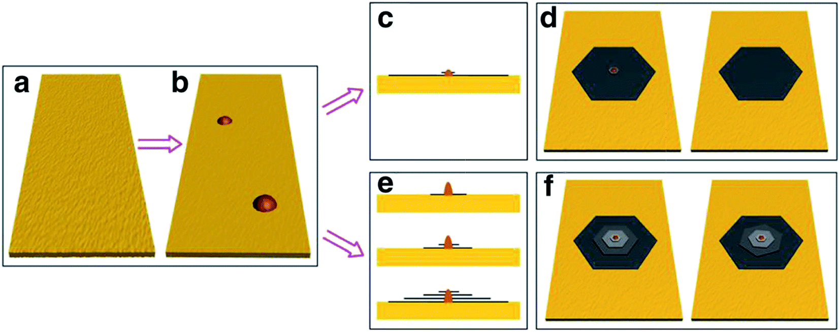 | ||
| Fig. 63 The proposed mechanism for graphene domain growth. (a) Smooth Cu foil was obtained by cleaning in a pretreatment step. (b) Formation of large oxide nanoparticles on the pretreated Cu foil. (c and d) In high hydrogen concentration conditions, large-single-crystal monolayer graphene was formed. (e and f) In low hydrogen concentration conditions, multilayer graphene was obtained. This figure has been adapted/reproduced from ref. 199 with permission from Springer. | ||
After the first layer of graphene emerges on the Cu substrate surface, a second graphene layer underneath the first layer possibly grows via a growth mechanism called the ‘penetration growth mechanism’, as proposed by Wu et al.200Fig. 64 shows a three-step process to attain bilayer graphene with great quality. The carbon atoms were transported to the interface of graphene and copper via an atom-exchange process, and these carbon atoms are responsible for the emergence of the second graphene layer growth underneath the first one. Once the second graphene layer was formed, the penetration of carbon atoms through the formed graphene was restricted. Hence, the third graphene layer growth was stopped. On the other hand, Wu and co-workers201 suggested that multilayer graphene was grown by diffusion through graphene edges to form a graphene stack, as shown in Fig. 65. The growth model described the growth mechanism model of subsequent graphene layer formation by the graphene nuclei. In this proposed model, the process is continued with the same manner but with a lower carbon feeding rate due to the constrained diffusion of carbon atoms into the lower graphene layer, which is opposite to the reports from previous studies.198,199 Thus, multilayer graphene contains smaller layers enclosed entirely on a larger graphene layer, as shown in Fig. 65(1).
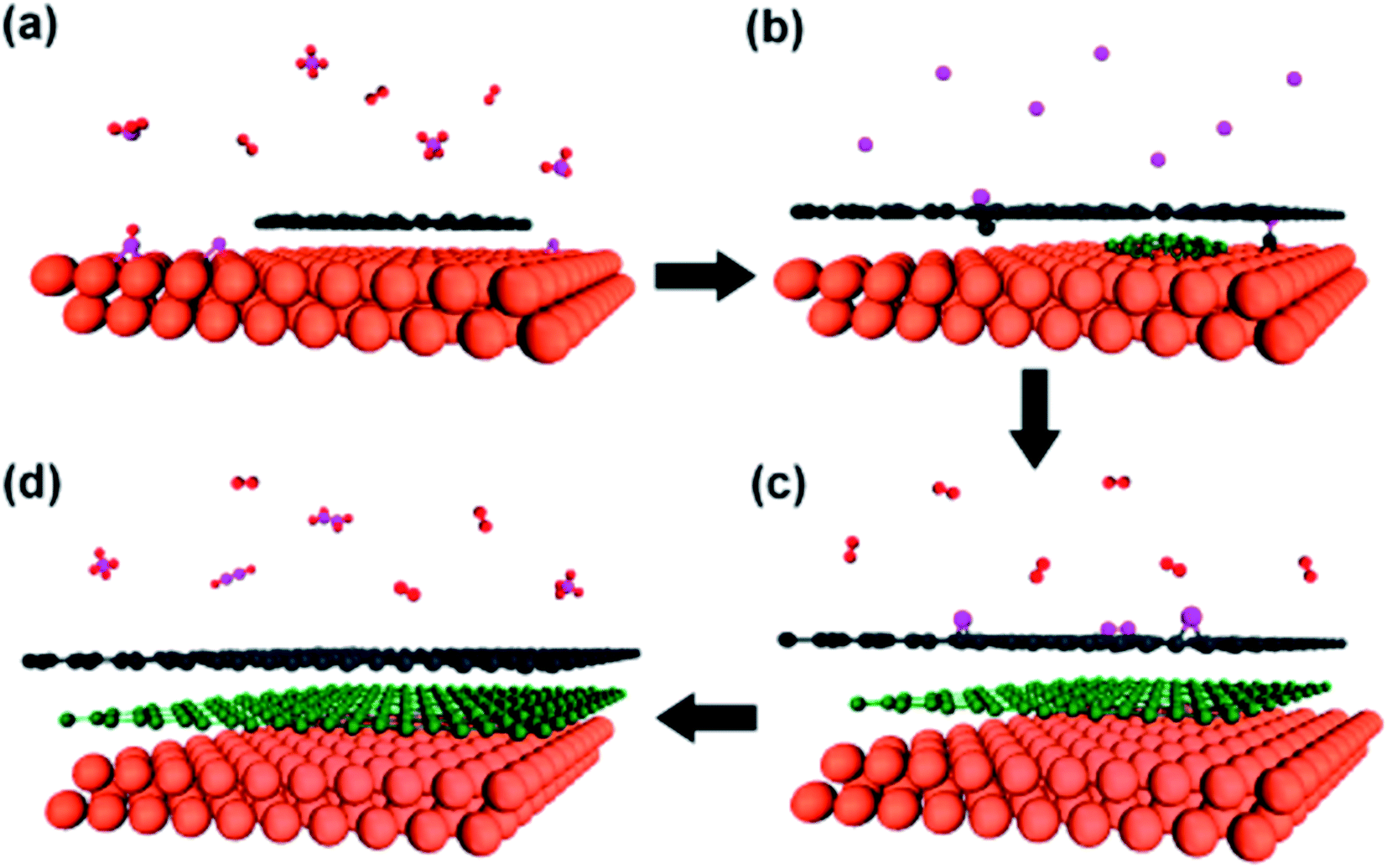 | ||
| Fig. 64 Schematic of a new bilayer graphene growth protocol. (a) Monolayer graphene is grown via standard CVD on Cu surface. (b) Carbon monomer intercalation occurs via a penetration mechanism. (c) Hydrogen gas is supplied to etch extra carbon species. (d) With desorption of the hydrocarbons, high-quality bilayer graphene is obtained. This figure has been adapted/reproduced from ref. 200 with permission from American Chemical Society. | ||
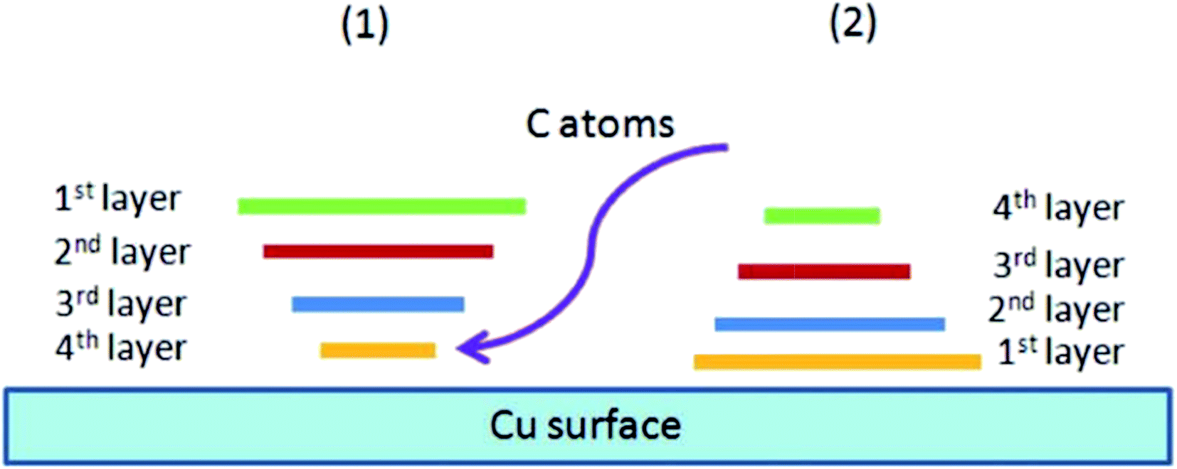 | ||
| Fig. 65 The proposed model in (1) compared to the model in (2) in terms of schematic side-view of the substrate and multilayer configuration in which the layer growth order, spatial arrangement and relative size are indicated. This figure has been adapted/reproduced from ref. 201 with permission from Wiley-VCH. | ||
Besides this, the synthesis of multilayer graphene enclosing copper nanoparticles in a huge scale was reported by Wang's group202 through a novel mechanism called the ‘coalescence mechanism’. The reported synthesis involved a single-step metal–organic CVD process to produce graphene/copper shell/core nanoparticles, as shown in Fig. 66. The encapsulated copper nanoparticles were produced by using analytical copper(II) acetylacetonate (Cu(acac)2) powder. Before the production of the graphene/Cu shell/core nanoparticles, there were 4 stages in the synthesis process: (1) synthesis and carrying of gaseous Cu(acac)2 to the reaction area, (2) deformation of Cu(acac)2 to produce small C/Cu nanoclusters, (3) bigger C/Cu agglomerates are formed from the aggregates of the C/Cun nanoclusters and (4) synthesis of the graphene/Cu shell/core nanoparticles (Fig. 66). This mechanism has different explanations regarding the dissolution and subsequent segregation and precipitation approach of carbon species with cobalt, iron or nickel nanoparticles to produce graphene/metal shell/core nanoparticles.203
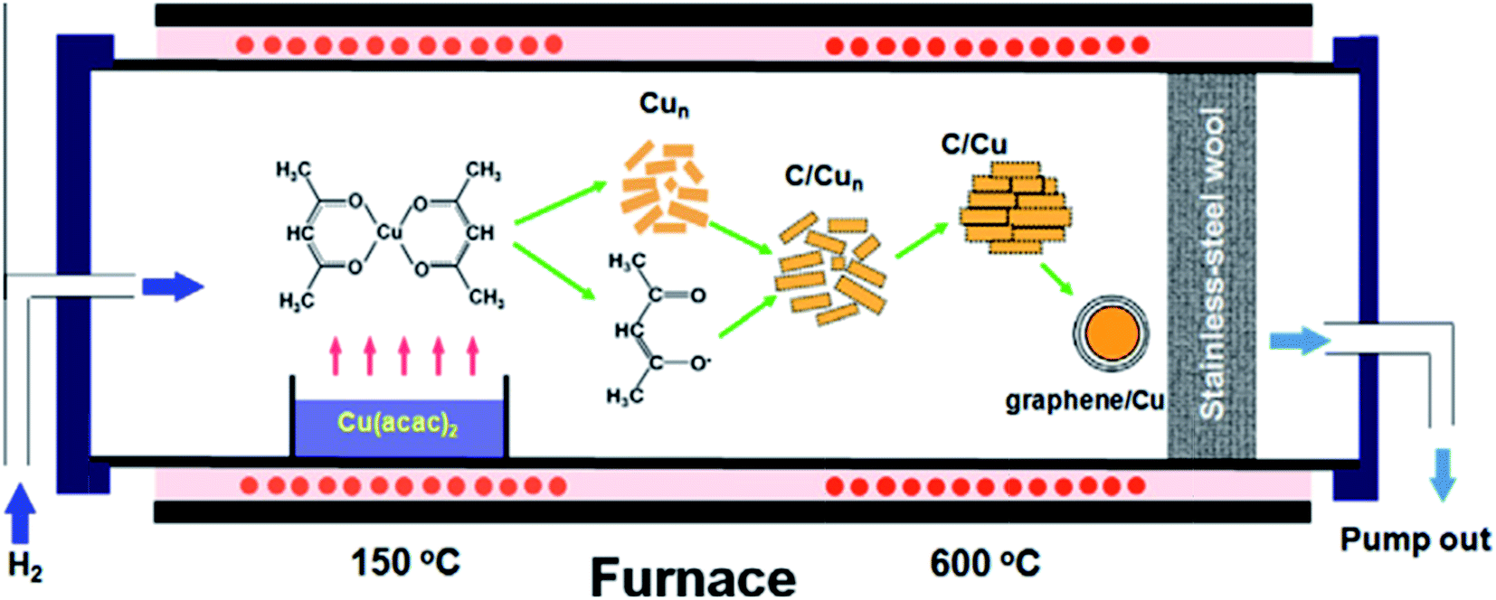 | ||
| Fig. 66 Schematic of the experimental set-up and the growth model for the graphene/Cu shell/core nanoparticles. This figure has been adapted/reproduced from ref. 202 with permission from Elsevier. | ||
In addition, plasma-enhanced (PE)-CVD is another route to synthesize graphene on a Cu substrate. Instead the synthesis of carbon nanowalls (CNWs) by PE-CVD is more common, where the formation of graphene was evidenced in the PE-CVD process at a comparably low reaction temperature, i.e. 500 °C.204 In contrast to the thermal CVD process, the dissociation of carbon precursors can hardly take place at this low reaction temperature. On the contrary, C2 radicals were formed in the plasma and deposited on the Cu surface for the emergence of a graphene layer in PE-CVD at a reaction temperature as low as 500 °C. Moreover, the C2 radicals maintain the growth rate of graphene even after formation of the initial layer. In the growth of the second graphene layer, the C2 and CH radicals accumulate at the edge of graphene, where the C2 radicals take part in the graphene growth, while the CH radicals hinder the expansion of the sp2 network. Besides PE-CVD, Wang's group demonstrated radio-frequency (RF)-PE-CVD205 to grow graphene layers on polycrystalline cobalt (Co). It was evidenced previously that graphene growth via the segregation and precipitation process typically occurs on metals with high carbon solubility, for example Ni, whereas the surface adsorption process happens on metals with low carbon solubility, like Cu. Thus, Co has a carbon solubility of 4.1 at%, which supports the segregation and precipitation process taking place preferably in the graphene growth on Co.206 However, a straightforward growth mechanism of carbon on the Co film surface is more dominant than the precipitation mechanism, as shown in Fig. 67. The proposed direct growth mechanism is very similar to the model of PE-CVD suggested by Tomo-o Terasawa and Koichiro Saiki.204
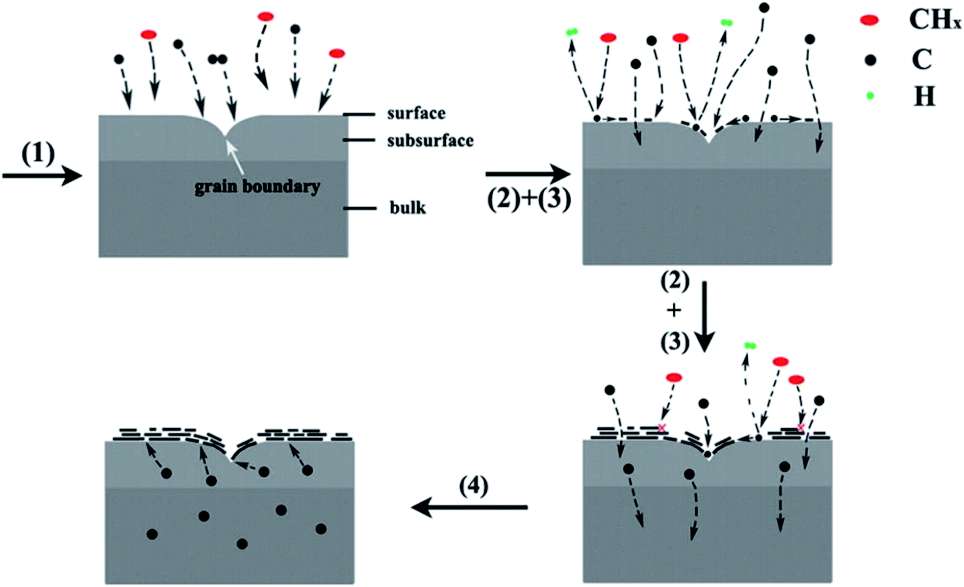 | ||
| Fig. 67 Schematic of the growth mechanism of graphene on polycrystalline Co film by radio frequency (RF)-PECVD. This figure has been adapted/reproduced from ref. 205 with permission from The Royal Society of Chemistry. | ||
Apart from this, a graphene layer was successfully synthesized on copper foil at atmospheric pressure via a CVD approach, as reported by Zhang et al.207Fig. 68 depicts the graphene formation under ambient pressure (AP) CVD conditions, which was elucidated by a combination of surface adsorption and epitaxial growth mechanisms. At first, the hydrocarbon was dissociated and move freely onto the copper foil. This was followed by the nucleation of the graphene grains, and graphene growth at the imperfections on the copper foil, such as folds and step edges. At the same time, carbon–copper alloyed nanoparticles were formed around graphene grains when carbon species were adsorbed on the copper surface. In Fig. 68(b), the dimension of the graphene grain was extended at the edge with enough carbon atoms supplied from the neighbouring C–Cu alloyed nanoparticles. With carbon species of great concentration, the second graphene layer grows atop the existing one via an epitaxial growth (Fig. 68(c)). Finally, a desired number of graphene layers can be synthesized based on controlling the growth duration.
 | ||
| Fig. 68 Schematic of the growth of graphene domains on copper foil under APCVD conditions: (a) nucleated graphene grain, (b) the size of the graphene grain increases, (c) the second layer grows on the first layer epitaxially and (d) few-layer graphene produced by a multi-epitaxial growth. This figure has been adapted/reproduced from ref. 207 with permission from Elsevier. | ||
8 Real-time and in situ observation of graphene growth
This technique is very useful to record a series of pictures or videos on the real-time growth of graphene at the nanometre scale. Low-pressure CVD was used to grow graphene in an environmental SEM (ESEM), and it was demonstrated that the growth at high temperature happened on a pre-melted and extremely dynamic copper surface, which was greatly affected by the copper grain orientation, temperature and atmosphere.208 Furthermore, in situ ESEM has the advantages for researchers to image the formation of graphene sheets on a metal substrate and to study the kinetics and mechanisms in a novel and unparalleled way.208Fig. 69 shows in situ SEM pictures recorded at 1000 °C during low-pressure (LP)-CVD conducted at different times duration. Besides, Yan et al.209 observed the dissolution of carbon in liquid copper (silver) at 1300 °C (1200 °C) and then precipitation out as graphene on liquid copper (silver) surface at 1130 °C or 1090 °C (1000 °C). Monolayer and multilayer graphene were formed in different manners, where multilayer graphene was observed with a hexagonal structure between the liquid copper surface and the monolayer graphene, and the multi-layers were grown beneath the monolayer graphene. | ||
| Fig. 69 In situ SEM images obtained at 1000 °C during LP-CVD growth, showing the nucleation and growth of carbon sheets (characterized by darker contrast). White arrows highlight nucleation events at the grain boundaries. t* corresponds to the induction period from C2H4 dosing until the first nucleation events can be detected. The growing graphene sheets are characterized by a dark contrast. Smooth contrast of the copper surface is due to a sublimation-induced surface buckling. Grain boundaries in the copper foil are highlighted by green dotted lines in the top-left image. Differences in contrast for different grains are due to electron channelling. This figure has been adapted/reproduced from ref. 208 with permission from American Chemical Society. | ||
A similar dissolution and precipitation mechanism was shown as well by Zhang et al.210 They reported success in the transformation of an amorphous carbon layer through the pyrolysis of solid carbon sources into graphene on silver nanoparticles (Ag NPs) and microparticles (Ag MPs) and copper nanoparticles (Cu NPs) with the addition of a moderate concentration of FeSO4 to avoid the synthesis of stretched graphene. In Fig. 70, the growth mechanism of a graphene nanoisland on a single metal nano-catalyst is elucidated to provides further understanding of mechanism.
 | ||
| Fig. 70 Schematic of the growth of the graphene nanoislands on a single metal nanocatalyst. This figure has been adapted/reproduced from ref. 210 with permission from Elsevier. Growth mechanism of the graphene nanoisland on a single metal nanocatalyst: (1) carbon atoms diffuse along the metal nanocatalyst surface; (2) catalytic growth of graphene nanoislands on the metal catalyst surface; (3) carbon atoms diffuse into the metal catalyst body; (4) carbon atoms migrate in the metal catalyst; (5) precipitation of carbon atoms when the solid solubility limit is reached; (6) growth of graphene nanoislands through realignment of carbon atoms. | ||
The heterogeneous nucleation and formation of graphene from Au nanoparticles seeds was observed using an in situ heating holder inside an aberration-corrected TEM.211 The edge growth and formation of a second layer beneath the first layer were seen at high magnification (Fig. 71). The mechanism was named as the ‘growth front propagation’ by Gong's group211 to describe the process of carbon deposition and indentation filling to keep a homogenous growth at the lowest energy.
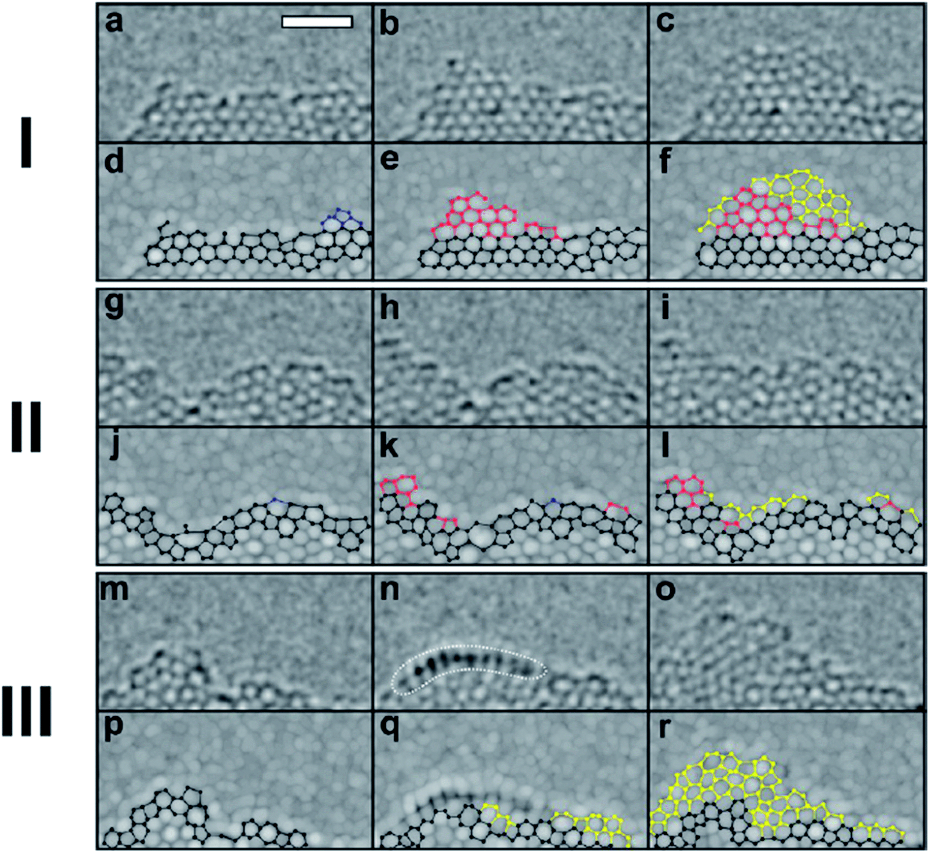 | ||
| Fig. 71 Another three sets of sequential AC-TEM images showing the edge growth and reconstruction of second-layer graphene at higher magnification: (a–c) carbon cluster deposition, (g–i) indentation filling and (m–o) back-folding of the edge. Time between frames is ∼10 s. (d–f), (j–l) and (p–r) Corresponding maximum filtered images with original edges coloured in black. Atoms attached to the edge in the next frames are coloured in red and yellow. Edge atoms to be etched are highlighted in blue. This figure has been adapted/reproduced from ref. 211 with permission from American Chemical Society. | ||
The presence of oxygen species in the low-pressure or atmospheric-pressure environments of CVD and Cu foils play an important role in graphene growth.212 Typically, most researchers use hydrogen to remove the oxide layer of copper foil in order to get pure Cu for graphene growth. However, Liang's group212 discovered that oxygen at Cu sites facilitates the formation of graphene, which has also been reported by many other researchers.213–218
9 Conclusions
Graphene research has surged dramatically since a graphene layer was first separated by utilizing the ‘Scotch tape’ method due to graphene's unique properties and features. Nowadays, the increasing amount of publication articles related to graphene research, as stated in the ISI Web of Knowledge, indicates that graphene is currently gaining large interest from all around the world. In this in-depth review, the recent developments in graphene research have been reviewed. Including the synthesis, characterization, transfer techniques and growth mechanisms of graphene layers. For graphene synthesis, we reviewed different forms of carbon precursor sources, such as solid, liquid, and gaseous, used to synthesize graphene sheets by CVD. Apart from the CVD technique, a variety of different novel synthesis methods have been presented in this review. The results show that these techniques are capable of synthesizing high-quality monolayer graphene sheets. However, more effort is still needed to improve on the graphene synthesis techniques in terms of scalability and cost effectiveness in order for them to be used in different industrial applications. Given the many different potential applications of graphene, i.e. photovoltaic cells, composite materials, battery storage and biosensors, graphene is expected to bring a large impact to the world of industry as well as to academy with its peculiar and extraordinary properties in the near future. Furthermore, Ruan et al.28 successfully demonstrated the use of food, insect and waste to synthesize graphene, which provides an excellent way to reduce waste on our planet by transforming the waste into graphene. Therefore, the large-scale production of graphene could utilize a huge amount of waste materials, which could be practised in industries in many countries.In addition, transferring graphene sheets to the desired substrate after the graphene growth is a crucial step as it could affect the quality of the transferred graphene and could represent the connecting platform between production and the application of graphene. Improper execution of the graphene transfer process can induce cracks and damage to the graphene layer, which will result in malfunction of the application devices. Therefore, a high quality of transferred graphene is the primary aim of all the transfer methods. Currently, the transfer-free growth method of graphene sheets shows promise as a straightforward synthesis of a graphene layer atop the desired substrate without the need for a catalyst and transfer of the graphene. Operating without this transfer step can simplify the graphene production process and reduce the chances of graphene degrading during the transfer step. However, this promising method is only in the preliminary stages, and further research and developments are necessary to apply it to industrial-scale production. Thus, the current graphene transfer process is still an essential process in the application of graphene. Besides, the cost of the transfer process is also a factor to be considered in the practical industrial applications.
We have also reviewed the characterization methods of graphene, including Raman spectroscopy, SEM, TEM, UV-vis spectroscopy, XRD and AFM. All these methods are the core characterization methods to investigate the properties of graphene sheets. Therefore, we have summarized each of the characterization methods for the ease of readers to determine the quality, number of graphene layers and surface morphology of the graphene films.
The growth mechanism of graphene layers could be classified into three different categories depending on the carbon solubility of the material. For high carbon solubility materials, graphene grows based on the segregation and precipitation process, whereas the surface adsorption process occurs for low carbon solubility materials. However, there is also an exception when graphene grows on a high carbon solubility of platinum, where the surface adsorption happens before the carbon precipitation process. In spite of the large number of graphene growth mechanisms reported, no single growth model can explain both single and multi-layered graphene growth. Gaining a greater understanding and controlling the synthesis process will be the key to further breakthroughs in these growth mechanisms. Therefore, the full exploration and reasonable cooperation between the world of industry and academy could establish a well-agreed graphene growth mechanism. The real-time and in situ observations can help researchers to gain a closer look at the changes inside the reaction chamber during the growth of graphene. Therefore, the collected information could be used to improve the existing graphene growth mechanism.
Acknowledgements
This work was funded by Ministry of Higher Education (MOHE) Malaysia under Fundamental Research Grant Scheme (FRGS) (Acc No. 9003-00415). The authors would like to thank all the team members in Institute of Nano Electronic Engineering.References
- M. J. Allen, V. C. Tung and R. B. Kaner, Honeycomb Carbon: A Review of Graphene, Chem. Rev., 2010, 110, 132–145 CrossRef CAS PubMed.
- A. K. Geim and K. S. Novoselov, The rise of graphene, Nat. Mater., 2007, 6, 183–191 CrossRef CAS.
- K. S. Novoselov, A. K. Geim, S. V. Morozov, D. Jiang, Y. Zhang and S. V. Dubonos, et al., Electric Field Effect in Atomically Thin Carbon Films, Science, 2004, 306, 666–669 CrossRef CAS.
- Royal THE, Academy S, Sciences OF, compiled by the Class for Physics of the Royal Swedish Academy of Sciences Graphene, R Swedish Acad Sci, 2010, 50005, 0–10.
- E. P. Randviir, D. a. C. Brownson and C. E. Banks, A decade of graphene research: production, applications and outlook, Mater. Today, 2014, 17, 426–432 CrossRef CAS.
- D. R. Cooper, B. D'Anjou, N. Ghattamaneni, B. Harack, M. Hilke and A. Horth, et al., Experimental review of graphene, ISRN Condens. Matter Phys., 2012, 2012, 56 Search PubMed.
- C. Riedl, Epitaxial Graphene on Silicon Carbide Surfaces: Growth, Characterization, Doping and Hydrogen Intercalation, 2010 Search PubMed.
- M. Orlita, C. Faugeras, P. Plochocka, P. Neugebauer, G. Martinez and D. K. Maude, et al. Approaching the dirac point in high-mobility multilayer epitaxial graphene, Phys. Rev. Lett., 2008, 101, 1–5 CrossRef PubMed.
- M. D. Stoller, S. Park, Y. Zhu, J. An and R. S. Ruoff, Graphene-based ultracapacitors, Nano Lett., 2008, 8, 3498–3502 CrossRef CAS.
- A. a Balandin, S. Ghosh, W. Bao, I. Calizo, D. Teweldebrhan and F. Miao, et al., Superior thermal conductivity of single-layer graphene, Nano Lett., 2008, 8, 902–907 CrossRef CAS.
- C. Lee, X. Wei, J. W. Kysar and J. Hone, Measurement of the elastic properties and intrinsic strength of monolayer graphene, Science, 2008, 321, 385–388 CrossRef CAS.
- R. R. Nair, P. Blake, A. N. Grigorenko, K. S. Novoselov, T. J. Booth and T. Stauber, et al., Fine Structure Constant Defines Visual Transparency of Graphene, Science, 2008, 320, 1308 CrossRef CAS PubMed.
- W. Choi, I. Lahiri, R. Seelaboyina and Y. S. Kang, Synthesis of Graphene and Its Applications: A Review, Critical Reviews in Solid State and Materials Sciences, Taylor & Francis, 2010 Search PubMed.
- C. Wonbong and L. Jo-won, Graphene: Synthesis and Applications, Taylor & Francis, 2012 Search PubMed.
- K. E. Whitener and P. E. Sheehan, Graphene synthesis, Diamond Relat. Mater., 2014, 46, 25–34 CrossRef CAS.
- V. Singh, D. Joung, L. Zhai, S. Das, S. I. Khondaker and S. Seal, Graphene based materials: past, present and future, Prog. Mater. Sci., 2011, 56, 1178–1271 CrossRef CAS.
- H. Wang and G. Yu, Direct CVD Graphene Growth on Semiconductors and Dielectrics for Transfer-Free Device Fabrication, Adv. Mater., 2016, 4956–4975 CrossRef CAS.
- J. Sun, Y. Zhang and Z. Liu, Direct Chemical Vapor Deposition Growth of Graphene on Insulating Substrates, ChemNanoMat, 2016, 2, 9–18 CrossRef CAS.
- P. Wu, W. Zhang, Z. Li and J. Yang, Mechanisms of graphene growth on metal surfaces: theoretical perspectives, Small, 2014, 10, 2136–2150 CrossRef CAS PubMed.
- Z. Yan, Z. W. Peng and J. M. Tour, Chemical Vapor Deposition of Graphene Single Crystals, Acc. Chem. Res., 2014, 47, 1327–1337 CrossRef CAS PubMed.
- C.-M. Seah, S.-P. Chai and A. R. Mohamed, Mechanisms of graphene growth by chemical vapour deposition on transition metals, Carbon, 2014, 70, 1–21 CrossRef CAS.
- P. R. Somani, S. P. Somani and M. Umeno, Planer nano-graphenes from camphor by CVD, Chem. Phys. Lett., 2006, 430, 56–59 CrossRef CAS.
- Z. Sun, Z. Yan, J. Yao, E. Beitler, Y. Zhu and J. M. Tour, Growth of graphene from solid carbon sources, Nature, 2010, 468, 549–552 CrossRef CAS PubMed.
- T. Wu, G. Ding, H. Shen, H. Wang, L. Sun and D. Jiang, et al., Triggering the Continuous Growth of Graphene Toward Millimeter-Sized Grains, Adv. Funct. Mater., 2013, 23, 198–203 CrossRef CAS.
- Z. Li, P. Wu, C. Wang, X. Fan, W. Zhang and X. Zhai, et al., Low-temperature growth of graphene by chemical vapor deposition using solid and liquid carbon sources, ACS Nano, 2011, 5, 3385–3390 CrossRef CAS PubMed.
- X. Gan, H. Zhou, B. Zhu, X. Yu, Y. Jia and B. Sun, et al., A simple method to synthesize graphene at 633 K by dechlorination of hexachlorobenzene on Cu foils, Carbon, 2012, 50, 306–310 CrossRef CAS.
- S. Sharma, G. Kalita, R. Hirano, S. M. Shinde, R. Papon and H. Ohtani, et al., Synthesis of graphene crystals from solid waste plastic by chemical vapor deposition, Carbon, 2014, 72, 66–73 CrossRef CAS.
- G. Ruan, Z. Sun, Z. Peng and J. M. Tour, Growth of graphene from food, insects, and waste, ACS Nano, 2011, 5, 7601–7607 CrossRef CAS.
- J.-K. Lee, S. Lee, Y.-I. Kim, J.-G. Kim, B.-K. Min and K.-I. Lee, et al., The seeded growth of graphene, Sci. Rep., 2014, 4, 5682 CrossRef CAS.
- H. Sun, J. Xu, C. Wang, G. Ge, Y. Jia and J. Liu, et al., Synthesis of large-area monolayer and bilayer graphene using solid coronene by chemical vapor deposition, Carbon, 2016, 108, 356–362 CrossRef CAS.
- E. Lee, H. C. Lee, S. B. Jo, H. Lee, N. S. Lee and C. G. Park, et al., Heterogeneous Solid Carbon Source-Assisted Growth of High-Quality Graphene via CVD at Low Temperatures, Adv. Funct. Mater., 2016, 26, 562–568 CrossRef CAS.
- P. W. Sutter, J.-I. Flege and E. a Sutter, Epitaxial graphene on ruthenium, Nat. Mater., 2008, 7, 406–411 CrossRef CAS.
- H. Ueta, M. Saida, C. Nakai, Y. Yamada, M. Sasaki and S. Yamamoto, Highly oriented monolayer graphite formation on Pt(1 1 1) by a supersonic methane beam, Surf. Sci., 2004, 560, 183–190 CrossRef CAS.
- S. Marchini, S. Günther and J. Wintterlin, Scanning tunneling microscopy of graphene on Ru(0001), Phys. Rev. B: Condens. Matter Mater. Phys., 2007, 76, 1–9 CrossRef.
- J. Coraux, A. T. N. Diaye, C. Busse, T. Michely, I. I. P. Institut and V. Uni, Structural Coherency of Graphene on Ir(111), Nano, 2008, 8, 565–570 CAS.
- N. R. Gall', E. V. Rut'kov and a. Y. Tontegode, Interaction of silver atoms with iridium and with a two-dimensional graphite film on iridium: adsorption, desorption, and dissolution, Phys. Solid State, 2004, 46, 371–377 CrossRef.
- G. Nandamuri, S. Roumimov and R. Solanki, Chemical vapor deposition of graphene films, Nanotechnology, 2010, 21, 145604 CrossRef CAS PubMed.
- A. Guermoune, T. Chari, F. Popescu, S. S. Sabri, J. Guillemette and H. S. Skulason, et al., Chemical vapor deposition synthesis of graphene on copper with methanol, ethanol, and propanol precursors, Carbon, 2011, 49, 4204–4210 CrossRef CAS.
- L. G. De Arco, Y. Zhang, A. Kumar and Z. Chongwu, Synthesis, Transfer, and Devices of Single- and Few-Layer Graphene by Chemical Vapor Deposition, IEEE Trans. Nanotechnol., 2009, 8, 135–138 Search PubMed.
- Z. Chen, W. Ren, B. Liu, L. Gao, S. Pei and Z.-S. Wu, et al., Bulk growth of mono- to few-layer graphene on nickel particles by chemical vapor deposition from methane, Carbon, 2010, 48, 3543–3550 CrossRef CAS.
- X. Li, C. W. Magnuson, A. Venugopal, J. An, J. W. Suk and B. Han, et al., Graphene Films with Large Domain Size by a Two-Step Chemical Vapor Deposition Process, Nano Lett., 2010, 10, 4328–4334 CrossRef CAS.
- Y. S. Kim, J. H. Lee, Y. D. Kim, S.-K. Jerng, K. Joo and E. Kim, et al., Methane as an effective hydrogen source for single-layer graphene synthesis on Cu foil by plasma enhanced chemical vapor deposition, Nanoscale, 2013, 5, 1221–1226 RSC.
- S.-H. Chan, S.-H. Chen, W.-T. Lin, M.-C. Li, Y.-C. Lin and C.-C. Kuo, Low-temperature synthesis of graphene on Cu using plasma-assisted thermal chemical vapor deposition, Nanoscale Res. Lett., 2013, 8, 285 CrossRef.
- Y. Kim, W. Song, S. Y. Lee, C. Jeon, W. Jung and M. Kim, et al., Low-temperature synthesis of graphene on nickel foil by microwave plasma chemical vapor deposition, Appl. Phys. Lett., 2011, 98, 263106–2631063 CrossRef CAS.
- J. Qi, L. Zhang, J. Cao, W. Zheng, X. Wang and J. Feng, Synthesis of graphene on a Ni film by radio-frequency plasma-enhanced chemical vapor deposition, Chin. Sci. Bull., 2012, 57, 3040–3044 CrossRef CAS.
- R. Addou, A. Dahal, P. Sutter and M. Batzill, Monolayer graphene growth on Ni(111) by low temperature chemical vapor deposition, Appl. Phys. Lett., 2012, 100, 0–3 CrossRef CAS.
- E. Cazzanelli, T. Caruso, M. Castriota, R. Marino a, a. Politano and G. Chiarello, et al., Spectroscopic characterization of graphene films grown on Pt(111) surface by chemical vapor deposition of ethylene, J. Raman Spectrosc., 2013, 44, 1393–1397 CrossRef CAS.
- R. R. Sagar, X. Zhang and C. Xiong, Growth of graphene on copper and nickel foils via chemical vapour deposition using ethylene, Mater. Res. Innovations, 2014, 18, S4706–S4710 CrossRef.
- N. S. Mueller, A. J. Morfa, D. Abou-ras, V. Oddone, T. Ciuk and M. Giersig, Growing graphene on polycrystalline copper foils by ultra-high vacuum chemical vapor deposition, Carbon, 2014, 78, 347–355 CrossRef CAS.
- Y. S. Woo, D. H. Seo, D. H. Yeon, J. Heo, H. J. Chung and A. Benayad, et al., Low temperature growth of complete monolayer graphene films on Ni-doped copper and gold catalysts by a self-limiting surface reaction, Carbon, 2013, 64, 315–323 CrossRef CAS.
- X. D. Chen, Z. Chen, W. S. Jiang, C. Zhang, J. Sun and H. Wang, et al., Fast Growth and Broad Applications of 25-Inch Uniform Graphene Glass, Adv. Mater., 2017, 29, 1603428–1603436 CrossRef.
- S. J. Le, C. Tang, H. J. Peng, L. Zhu, X. B. Cheng and J. Q. Huang, et al., 3D Mesoporous Graphene: CVD Self-Assembly on Porous Oxide Templates and Applications in High-Stable Li–S Batteries, Small, 2015, 11, 5243–5252 CrossRef.
- C. Tang, B.-Q. Li, Q. Zhang, L. Zhu, H.-F. Wang and J.-L. Shi, et al., CaO-Templated Growth of Hierarchical Porous Graphene for High-Power Lithium–Sulfur Battery Applications, Adv. Funct. Mater., 2016, 26, 577–585 CrossRef CAS.
- M.-Q. Zhao, Q. Zhang, J.-Q. Huang, G.-L. Tian, J.-Q. Nie and H.-J. Peng, et al., Unstacked double-layer templated graphene for high-rate lithium–sulphur batteries, Nat. Commun., 2014, 5, 3410 CrossRef PubMed.
- L. Shi, K. Chen, R. Du, A. Bachmatiuk, M. H. Rümmeli and M. K. Priydarshi, et al., Direct Synthesis of Few-Layer Graphene on NaCl Crystals, Small, 2015, 11, 6302–6308 CrossRef CAS.
- K. Coleman, M. Tynan, D. Johnson and B. Dobson, Formation of 3D Graphene Foams on Soft Templated Metal Monoliths, Nanoscale, 2016, 13303–13310 Search PubMed.
- L. Shi, K. Chen, R. Du, A. Bachmatiuk, M. H. Rümmeli and K. Xie, et al., Scalable Seashell-Based Chemical Vapor Deposition Growth of Three-Dimensional Graphene Foams for Oil–Water Separation, J. Am. Chem. Soc., 2016, 138, 6360–6363 CrossRef CAS.
- Z. Chen, W. Ren, L. Gao, B. Liu, S. Pei and H.-M. Cheng, Three-dimensional flexible and conductive interconnected graphene networks grown by chemical vapour deposition, Nat. Mater., 2011, 10, 424–428 CrossRef CAS PubMed.
- B. H. Min, D. W. Kim, K. H. Kim, H. O. Choi, S. W. Jang and H. T. Jung, Bulk scale growth of CVD graphene on Ni nanowire foams for a highly dense and elastic 3D conducting electrode, Carbon, 2014, 80, 446–452 CrossRef CAS.
- Y. Yao, Z. Li, Z. Lin, K.-S. Moon, J. Agar and C. Wong, Controlled Growth of Multilayer, Few-Layer, and Single-Layer Graphene on Metal Substrates, J. Phys. Chem. C, 2011, 115, 5232–5238 CrossRef CAS.
- J. Campos-Delgado, A. R. Botello-Méndez, G. Algara-Siller, B. Hackens, T. Pardoen and U. Kaiser, et al., VD synthesis of mono- and few-layer graphene using alcohols at low hydrogen concentration and atmospheric pressure, Chem. Phys. Lett., 2013, 584, 142–146 CrossRef CAS.
- G.-P. Dai, P. H. Cooke and S. Deng, Direct growth of graphene films on TEM nickel grids using benzene as precursor, Chem. Phys. Lett., 2012, 531, 193–196 CrossRef CAS.
- Z. Li, P. Wu, C. Wang, X. Fan, W. Zhang and X. Zhai, et al., Low-temperature growth of graphene by chemical vapor deposition using solid and liquid carbon sources, ACS Nano, 2011, 5, 3385–3390 CrossRef CAS.
- S. Gadipelli, I. Calizo, J. Ford, G. Cheng, A. R. Hight Walker and T. Yildirim, A highly practical route for large-area, single layer graphene from liquid carbon sources such as benzene and methanol, J. Mater. Chem., 2011, 21, 16057 RSC.
- R. K. Paul, S. Badhulika, S. Niyogi, R. C. Haddon, V. M. Boddu and C. Costales-Nieves, et al., The production of oxygenated polycrystalline graphene by one-step ethanol-chemical vapor deposition, Carbon, 2011, 49, 3789–3795 CrossRef CAS.
- A. Guermoune, T. Chari, F. Popescu, S. S. Sabri, J. Guillemette and H. S. Skulason, et al., Chemical vapor deposition synthesis of graphene on copper with methanol, ethanol, and propanol precursors, Carbon, 2011, 49, 4204–4210 CrossRef CAS.
- N. Lisi, F. Buonocore, T. Dikonimos, E. Leoni, G. Faggio and G. Messina, et al., Rapid and highly efficient growth of graphene on copper by chemical vapor deposition of ethanol, Thin Solid Films, 2014, 571, 139–144 CrossRef CAS.
- A. Srivastava, C. Galande, L. Ci, L. Song, C. Rai and D. Jariwala, et al., Novel Liquid Precursor-Based Facile Synthesis of Large-Area Continuous, Single, and Few-Layer Graphene Films, Chem. Mater., 2010, 22, 3457–3461 CrossRef CAS.
- C. M. Orofeo, H. Ago, B. Hu and M. Tsuji, Synthesis of large area, homogeneous, single layer graphene films by annealing amorphous carbon on Co and Ni, Nano Res., 2011, 4, 531–540 CrossRef CAS.
- C. Li, D. Li, J. Yang, X. Zeng and W. Yuan, Preparation of Single- and Few-Layer Graphene Sheets Using Co Deposition on SiC Substrate, J. Nanomater., 2011, 2011(319624), 7 Search PubMed.
- H. Tanaka, R. Arima, M. Fukumori, D. Tanaka, R. Negishi and Y. Kobayashi, et al., Method for Controlling Electrical Properties of Single-Layer Graphene Nanoribbons via Adsorbed Planar Molecular Nanoparticles, Sci. Rep., 2015, 5, 12341 CrossRef CAS.
- M. Choucair, P. Thordarson and J. a Stride, Gram-scale production of graphene based on solvothermal synthesis and sonication, Nat. Nanotechnol., 2009, 4, 30–33 CrossRef CAS.
- D. K. Singh, P. K. Iyer and P. K. Giri, Improved Chemical Synthesis of Graphene Using a Safer Solvothermal Route, Int. J. Nanosci., 2011, 10, 39–42 CrossRef CAS.
- M. Alanyalıoğlu, J. J. Segura, J. Oró-Solè and N. Casañ-Pastor, The synthesis of graphene sheets with controlled thickness and order using surfactant-assisted electrochemical processes, Carbon, 2012, 50, 142–152 CrossRef.
- L. Yu, S. Yasuda and K. Murakoshi, Synthesis of Nanometer Size Single Layer Graphene by Moderate Electrochemical Exfoliation, Trans. Mater. Res. Soc. Jpn., 2012, 37, 209–212 CrossRef CAS.
- C. Berger, Z. Song, T. Li, X. Li, A. Y. Ogbazghi and R. Feng, et al., Ultrathin Epitaxial Graphite: 2D Electron Gas Properties and a Route toward Graphene-based Nanoelectronics, J. Phys. Chem. B, 2004, 108, 19912–19916 CrossRef CAS.
- V. S. Kiselov, P. M. Lytvyn, A. S. Nikolenko, V. V. Strelchuk, Y. Y. Stubrov and M. Tryus, et al., The growth of weakly coupled graphene sheets from silicon carbide powder, Semicond. Phys., Quantum Electron. Optoelectron., 2014, 17, 301–307 CrossRef.
- X. Z. Yu, C. G. Hwang, C. M. Jozwiak, A. Köhl, A. K. Schmid and A. Lanzara, New synthesis method for the growth of epitaxial graphene, J. Electron Spectrosc. Relat. Phenom., 2011, 184, 100–106 CrossRef CAS.
- A. E. Del Rio-Castillo, C. Merino, E. Díez-Barra and E. Vázquez, Selective suspension of single layer graphene mechanochemically exfoliated from carbon nanofibres, Nano Res., 2014, 7, 963–972 CrossRef.
- Y. Wang, H. Sun, R. Zhang, S. Yu and J. Kong, Large scale templated synthesis of single-layered graphene with a high electrical capacitance, Carbon, 2013, 53, 245–251 CrossRef CAS.
- C. Gomez-Navarro, Electronic transport properties of individual chemically reduced graphene oxide sheets, Nano Lett., 2007, 7, 3499–3503 CrossRef CAS.
- H. B. Peng, X. Lu, R. Cheng, Q. Wang, Y. T. Zhao and W. Yuan, et al., Formation of monolayer graphene on a basal HOPG surface irradiated with Xe ions, Nucl. Instrum. Methods Phys. Res., Sect. B, 2013, 307, 127–130 CrossRef CAS.
- S. Aminalragia Giamini, J. Marquez-Velasco, I. Sakellis, P. Tsipas, N. Kelaidis and D. Tsoutsou, et al., Experimental investigation of metallic thin film modification of nickel substrates for chemical vapor deposition growth of single layer graphene at low temperature, Appl. Surf. Sci., 2016, 385, 554–561 CrossRef CAS.
- M. Xu, D. Fujita, K. Sagisaka, E. Watanabe and N. Hanagata, Production of Extended Single-Layer Graphene, ACS Nano, 2011, 5, 1522–1528 CrossRef CAS.
- J.-H. Gao, N. Ishida, I. Scott and D. Fujita, Controllable growth of single-layer graphene on a Pd(111) substrate, Carbon, 2012, 50, 1674–1680 CrossRef CAS.
- R. Tatti, L. Aversa, R. Verucchi, E. Cavaliere, G. Garberoglio and N. M. Pugno, et al., Synthesis of single layer graphene on Cu(111) by C60 supersonic molecular beam epitaxy, RSC Adv., 2016, 6, 37982–37993 RSC.
- G. S. Shmavonyan, G. G. Sevoyan and V. M. Aroutiounian, Enlarging the Surface Area of Monolayer Graphene Synthesized by Mechanical Exfoliation, Arm. J. Phys., 2013, 6, 1–6 CAS.
- W. Choi, I. Lahiri, R. Seelaboyina and Y. S. Kang, Synthesis of Graphene and Its Applications: A Review, Crit. Rev. Solid State Mater. Sci., 2010, 35, 52–71 CrossRef CAS.
- L. Zhu, X. Zhao, Y. Li, X. Yu, C. Li and Q. Zhang, High-quality production of graphene by liquid-phase exfoliation of expanded graphite, Mater. Chem. Phys., 2013, 137, 984–990 CrossRef CAS.
- C. Liu, G. Hu and H. Gao, Preparation of few-layer and single-layer graphene by exfoliation of expandable graphite in supercritical N,N-dimethylformamide, J. Supercrit. Fluids, 2012, 63, 99–104 CrossRef CAS.
- L. Padrela, M. A. Rodrigues, S. P. Velaga, H. A. Matos and E. G. de Azevedo, Formation of indomethacin–saccharin cocrystals using supercritical fluid technology, Eur. J. Pharm. Sci., 2009, 38, 9–17 CrossRef CAS.
- S. Yumin, P. June, J. K. Yu, S. Maeng-Je and H. Seunghun, Synthesis of Graphene Layers Using Graphite Dispersion in Aqueous Surfactant Solutions, J. Korean Phys. Soc., 2011, 58, 938 CrossRef.
- Z. Chen, T. Huang, B. C. Jin, J. Hu, H. Lu and S. Nutt, High yield synthesis of single-layer graphene microsheets with dimensional control, Carbon, 2014, 68, 167–174 CrossRef CAS.
- A. V. Korobeinyk, R. L. D. Whitby, J. P. Salvage and S. V. Mikhalovsky, Exfoliated production of single- and multi-layer graphenes and carbon nanofibres from the carbonisation of a co-polymer, Carbon, 2012, 50, 2018–2025 CrossRef CAS.
- A. Gupta, G. Chen, P. Joshi, S. Tadigadapa and P. C. Eklund, Raman Scattering from High-Frequency Phonons in Supported n-Graphene Layer Films, Nano Lett., 2006, 6, 2667–2673 CrossRef CAS PubMed.
- K. S. Kim, Y. Zhao, H. Jang, S. Y. Lee, J. M. Kim and K. S. Kim, et al., Large-scale pattern growth of graphene films for stretchable transparent electrodes, Nature, 2009, 457, 706–710 CrossRef CAS.
- Y. Lee, S. Bae, H. Jang, S. Jang, S.-E. Zhu and S. H. Sim, et al., Wafer-Scale Synthesis and Transfer of Graphene Films, Nano Lett., 2010, 10, 490–493 CrossRef CAS.
- A. Reina, X. Jia, J. Ho, D. Nezich, H. Son and V. Bulovic, et al., Large area, few-layer graphene films on arbitrary substrates by chemical vapor deposition, Nano Lett., 2009, 9, 30–35 CrossRef CAS.
- A. Reina, H. Son, L. Jiao, B. Fan, M. S. Dresselhaus and Z. Liu, et al., Transferring and Identification of Single- and Few-Layer Graphene on Arbitrary Substrates, J. Phys. Chem. C, 2008, 112, 17741–17744 CrossRef.
- S. Bae, H. Kim, Y. Lee, X. Xu, J.-S. Park and Y. Zheng, et al., Roll-to-roll production of 30-inch graphene films for transparent electrodes, Nat. Nanotechnol., 2010, 5, 574–578 CrossRef CAS.
- Z.-Y. Juang, C.-Y. Wu, A.-Y. Lu, C.-Y. Su, K.-C. Leou and F.-R. Chen, et al., Graphene synthesis by chemical vapor deposition and transfer by a roll-to-roll process, Carbon, 2010, 48, 3169–3174 CrossRef CAS.
- S. J. Byun, H. Lim, G. Y. Shin, T. H. Han, S. H. Oh, J. H. Ahn, H. C. Choi and T. W. Lee, Graphene Converted from Polymers, J. Phys. Chem. Lett., 2011, 2, 493–497 CrossRef CAS.
- A. Ismach, C. Druzgalski, S. Penwell, A. Schwartzberg, M. Zheng and A. Javey, et al., Direct chemical vapor deposition of graphene on dielectric surfaces, Nano Lett., 2010, 10, 1542–1548 CrossRef CAS PubMed.
- M. Her, R. Beams and L. Novotny, Graphene transfer with reduced residue, Phys. Lett. A, 2013, 377, 1455–1458 CrossRef CAS.
- W.-H. Lin, T.-H. Chen, J.-K. Chang, J.-I. Taur, Y.-Y. Lo and W.-L. Lee, et al., A Direct and Polymer-Free Method for Transferring Graphene Grown by Chemical Vapor Deposition to Any Substrate, ACS Nano, 2014, 8, 1784–1791 CrossRef CAS.
- G. Borin Barin, Y. Song, I. de Fátima Gimenez, A. G. Souza Filho, L. S. Barreto and J. Kong, Optimized graphene transfer: influence of polymethylmethacrylate (PMMA) layer concentration and baking time on graphene final performance, Carbon, 2015, 84, 82–90 CrossRef CAS.
- X. Liang, B. a. Sperling, I. Calizo, G. Cheng, C. A. Hacker and Q. Zhang, et al., Toward clean and crackless transfer of graphene, ACS Nano, 2011, 5, 9144–9153 CrossRef.
- C. J. An, S. J. Kim, H. O. Choi, D. W. Kim, S. W. Jang and M. L. Jin, et al., Ultraclean transfer of CVD-grown graphene and its application to flexible organic photovoltaic cells, J. Mater. Chem. A, 2014, 2, 20474–20480 RSC.
- K. S. Novoselov, V. I. Fal'ko, L. Colombo, P. R. Gellert, M. G. Schwab and K. Kim, A roadmap for graphene, Nature, 2012, 490, 192–200 CrossRef CAS.
- H. Yang, J. Heo, S. Park, H. J. Song, D. H. Seo and K.-E. Byun, et al., Graphene Barristor, a Triode Device with a Gate-Controlled Schottky Barrier, Science, 2012, 336, 1140–1143 CrossRef CAS.
- M. Liu, X. Yin, E. Ulin-Avila, B. Geng, T. Zentgraf and L. Ju, et al., A graphene-based broadband optical modulator, Nature, 2011, 474, 64–67 CrossRef CAS.
- L. Gao, G.-X. Ni, Y. Liu, B. Liu, A. H. Castro Neto and K. P. Loh, Face-to-face transfer of wafer-scale graphene films, Nature, 2013, 505, 190–194 CrossRef.
- X. Li, W. Cai, J. An, S. Kim, J. Nah and D. Yang, et al., Large-area synthesis of high-quality and uniform graphene films on copper foils, Science, 2009, 324, 1312–1314 CrossRef CAS.
- L. Gao, W. Ren, J. Zhao, L.-P. Ma, Z. Chen and H.-M. Cheng, Efficient growth of high-quality graphene films on Cu foils by ambient pressure chemical vapor deposition, Appl. Phys. Lett., 2010, 97, 183109 CrossRef.
- L. Gao, W. Ren, H. Xu, L. Jin, Z. Wang and T. Ma, et al., Repeated growth and bubbling transfer of graphene with millimetre-size single-crystal grains using platinum, Nat. Commun., 2012, 3, 699 CrossRef.
- J. Kang, S. Hwang, J. H. Kim, M. H. Kim, J. Ryu and S. J. Seo, et al., Efficient transfer of large-area graphene films onto rigid substrates by hot pressing, ACS Nano, 2012, 6, 5360–5365 CrossRef CAS.
- F. M. Kafiah, Z. Khan, A. Ibrahim, R. Karnik, M. Atieh and T. Laoui, Monolayer graphene transfer onto polypropylene and polyvinylidenedifluoride microfiltration membranes for water desalination, Desalination, 2016, 388, 29–37 CrossRef CAS.
- B. N. Chandrashekar, B. Deng, A. S. Smitha, Y. Chen, C. Tan and H. Zhang, et al., Roll-to-Roll Green Transfer of CVD Graphene onto Plastic for a Transparent and Flexible Triboelectric Nanogenerator, Adv. Mater., 2015, 27, 5210–5216 CrossRef CAS.
- P. Gupta, P. D. Dongare, S. Grover, S. Dubey, H. Mamgain and A. Bhattacharya, et al., A facile process for soak-and-peel delamination of CVD graphene from substrates using water, Sci. Rep., 2014, 4, 3882 CrossRef.
- K. Tang, X. Wang, W. Yan, J. Yu and R. Xu, Fabrication of superhydrophilic Cu2O and CuO membranes, J. Membr. Sci., 2006, 286, 279–284 CrossRef CAS.
- N. J. Shirtcliffe, G. McHale, M. I. Newton and C. C. Perry, Wetting and wetting transitions on copper-based super-hydrophobic surfaces, Langmuir, 2005, 21, 937–943 CrossRef CAS.
- S. Y. Yang, J. G. Oh, D. Y. Jung, H. Choi, C. H. Yu and J. Shin, et al., Metal-Etching-Free Direct Delamination and Transfer of Single-Layer Graphene with a High Degree of Freedom, Small, 2015, 11, 175–181 CrossRef CAS.
- Y. Ren, C. Zhu, W. Cai, H. Li, Y. Hao and Y. Wu, et al., An Improved Method For Transferring Graphene Grown By Chemical Vapor Deposition, Nano, 2012, 7, 1150001 CrossRef.
- X. Yang, H. Peng, Q. Xie, Y. Zhou and Z. Liu, Clean and efficient transfer of CVD-grown graphene by electrochemical etching of metal substrate, J. Electroanal. Chem., 2013, 688, 243–248 CrossRef CAS.
- G. J. M. Fechine, I. Martin-Fernandez, G. Yiapanis, R. Bentini, E. S. Kulkarni and R. V. Bof de Oliveira, et al., Direct dry transfer of chemical vapor deposition graphene to polymeric substrates, Carbon, 2015, 83, 224–231 CrossRef CAS.
- L. G. P. Martins, Y. Song, T. Zeng, M. S. Dresselhaus, J. Kong and P. T. Araujo, Direct transfer of graphene onto flexible substrates, Proc. Natl. Acad. Sci. U. S. A., 2013, 110, 17762–17767 CrossRef CAS.
- B. Milan, K. Martin, J. Ivan, K. Ladislav and F. Otakar, Experimental Study of PIB-Based CVD Graphene Transfer Efficiency, in NANOCON, 2015, vol. 2015, pp. 14–19 Search PubMed.
- J. Song, F. Kam, R. Png, W. Seah, J. Zhuo and G. Lim, et al., A general method for transferring graphene onto soft surfaces, Nat. Nanotechnol., 2013, 8, 356–362 CrossRef CAS.
- C. S. Chen and C. K. Hsieh, An easy, low-cost method to transfer large-scale graphene onto polyethylene terephthalate as a transparent conductive flexible substrate, Thin Solid Films, 2014, 570, 595–598 CrossRef CAS.
- D. L. Mafra, T. Ming and J. Kong, Facile graphene transfer directly to target substrates with a reusable metal catalyst, Nanoscale, 2015, 7, 14807–14812 RSC.
- S. Jiang, Y. Zeng, W. Zhou, X. Miao and Y. Yu, One-Minute Room-Temperature Transfer-Free Production of Mono- and Few-Layer Polycrystalline Graphene on Various Substrates, Nat. Publ. Gr., 2016, 1–14 Search PubMed.
- Raman Spectroscopy for Nanomaterials Characterization, ed. C. S. S. R. Kumar, Springer Berlin Heidelberg, Berlin, Heidelberg, 2012, DOI:10.1007/978-3-642-20620-7.
- D. Yoon, H. Moon and H. Cheong, Variations in the Raman Spectrum as a Function of the Number of Graphene Layers, J. Korean Phys. Soc., 2009, 55, 1299–1303 CrossRef CAS.
- W. Li, H. Zhang, C. Wang, Y. Zhang, L. Xu and K. Zhu, et al., Raman characterization of aligned carbon nanotubes produced by thermal decomposition of hydrocarbon vapor, Appl. Phys. Lett., 1997, 70, 2684 CrossRef CAS.
- P. C. Eklund, J. M. Holden and R. A. Jishi, Vibrational modes of carbon nanotubes; Spectroscopy and theory, Carbon, 1995, 33, 959–972 CrossRef CAS.
- Y. Wang, Z. Ni, T. Yu, Z. X. Shen, H. Wang and Y. Wu, et al., Raman Studies of Monolayer Graphene: The Substrate Effect, J. Phys. Chem. C, 2008, 112, 10637–10640 CrossRef CAS.
- A. Dato, V. Radmilovic, Z. Lee, J. Phillips and M. Frenklach, Substrate-Free Gas-Phase Synthesis of Graphene Sheets, Nano Lett., 2008, 8, 2012–2016 CrossRef CAS.
- W. Li, C. Tan, M. A. Lowe, H. D. Abruña and D. C. Ralph, Electrochemistry of individual monolayer graphene sheets, ACS Nano, 2011, 5, 2264–2270 CrossRef CAS.
- a. C. Ferrari, J. C. Meyer, V. Scardaci, C. Casiraghi, M. Lazzeri and F. Mauri, et al., Raman Spectrum of Graphene and Graphene Layers, Phys. Rev. Lett., 2006, 97, 187401 CrossRef CAS.
- B. Voutou, E. Stefanaki and K. Giannakopoulos, Electron Microscopy: The Basics, Phys. Adv. Mater. Winter School, 2008, 1–11 Search PubMed.
- A. M. O. L. Alyamani, FE-SEM Characterization of Some Nanomaterial, in Scanning Electron Microscopy, ed. V. Kazmiruk, InTech, 2012, pp. 463–472 Search PubMed.
- C. Xiu-Yun, Graphene-like nanosheets synthesized by natural flaky graphite in Shandong, China, Int. Nano Lett., 2013, 3, 6–10 CrossRef.
- K. T. Van, D. S. Kwak, Y. J. Kwon, H. Y. Cho, T. N. Huan and H. Chung, et al., Direct production of highly conductive graphene with a low oxygen content by a microwave-assisted solvothermal method, Chem. Eng. J., 2013, 232, 346–355 CrossRef.
- Y. Gui, J. Yuan, W. Wang, J. Zhao, J. Tian and B. Xie, Facile solvothermal synthesis and gas sensitivity of graphene/WO3 nanocomposites, Materials, 2014, 7, 4587–4600 CrossRef.
- R. Hawaldar, P. Merino, M. R. Correia, I. Bdikin, J. Grácio and J. Méndez, et al., Large-area high-throughput synthesis of monolayer graphene sheet by Hot Filament Thermal Chemical Vapor Deposition, Sci. Rep., 2012, 2, 2–10 Search PubMed.
- C. Dang, Q. L. Che, B. L. Gao, L. Li and B. B. Wang, Growth, photoluminescence and thermal conductance of graphene-like nanoflakes grown on copper foils in methane environment, Mater. Sci. Semicond. Process., 2014, 27, 97–102 CrossRef CAS.
- R. Kumar, A. K. Sharma, M. Bhatnagar, B. R. Mehta and S. Rath, Antireflection properties of graphene layers on planar and textured silicon surfaces, Nanotechnology, 2013, 24, 165402 CrossRef.
- Z. Tu, Z. Liu, Y. Li, F. Yang, L. Zhang and Z. Zhao, et al., Controllable growth of 1–7 layers of graphene by chemical vapour deposition, Carbon, 2014, 73, 252–258 CrossRef CAS.
- K. Takahashi, K. Yamada, H. Kato, H. Hibino and Y. Homma, In situ scanning electron microscopy of graphene growth on polycrystalline Ni substrate, Surf. Sci., 2012, 606, 728–732 CrossRef CAS.
- C. Oshima, Ultra-thin epitaxial films of graphite and hexagonal boron nitride on solid surfaces, J. Phys.: Condens. Matter, 1997, 9, 1–20 CrossRef CAS.
- S. Chen, L. Brown, M. Levendorf, W. Cai, S. Y. Ju and J. Edgeworth, et al., Oxidation resistance of graphene-coated Cu and Cu/Ni alloy, ACS Nano, 2011, 5, 1321–1327 CrossRef CAS.
- P. Zeller, S. Dänhardt, S. Gsell, M. Schreck and J. Wintterlin, Scalable synthesis of graphene on single crystal Ir(111) films, Surf. Sci., 2012, 5, 10–15 Search PubMed.
- W. Wu, Q. Yu, P. Peng, Z. Liu, J. Bao and S.-S. Pei, Control of thickness uniformity and grain size in graphene films for transparent conductive electrodes, Nanotechnology, 2011, 23, 35603 CrossRef.
- H. Ma, K.-J. Shieh and T. X. Qiao, Study of Transmission Electron Microscopy (TEM) and Scanning Electron Microscopy (SEM), Nat. Sci., 2006, 4, 14–22 Search PubMed.
- A. W. Robertson and J. H. Warner, Atomic resolution imaging of graphene by transmission electron microscopy, Nanoscale, 2013, 5, 4079 RSC.
- F. Banhart, J. Kotakoski and A. V. Krasheninnikov, Structural defects in graphene, ACS Nano, 2011, 5, 26–41 CrossRef CAS.
- H. Wang, G. Wang, P. Bao, S. Yang, W. Zhu and X. Xie, et al., Controllable synthesis of submillimeter single-crystal monolayer graphene domains on copper foils by suppressing nucleation, J. Am. Chem. Soc., 2012, 134, 3627–3630 CrossRef CAS.
- Ultraviolet-visible spectroscopy, http://www.princeton.edu/%7Eachaney/tmve/wiki100k/docs/Ultraviolet-visible_spectroscopy.html, accessed 24 Aug, 2014.
- UV-vis Absorption Spectroscopy – Theory, http://teaching.shu.ac.uk/hwb/chemistry/tutorials/molspec/uvvisab1.html, accessed 24 Aug, 2014.
- S. Behera, S. Ghanty, F. Ahmad, S. Santra and S. Banerjee, UV-visible Spectrophotometric Method Development and Validation of Assay of Paracetamol Tablet Formulation, J. Anal. Bioanal. Tech., 2012, 3, 151–156 Search PubMed.
- D. Pavia, G. Lampman, G. Kriz and J. Vyvyan, Introduction to Spectroscopy, Brooks/Cole Cengage Learning, 4th edn, 2008 Search PubMed.
- The Royal Society of Chemistry, Ultraviolet/visible spectroscopy, 92–115.
- J. R. Potts, D. R. Dreyer, C. W. Bielawski and R. S. Ruoff, Graphene-based polymer nanocomposites, Polymer, 2011, 52, 5–25 CrossRef CAS.
- T. V. Cuong, V. H. Pham, Q. T. Tran, S. H. Hahn, J. S. Chung and E. W. Shin, et al., Photoluminescence and Raman studies of graphene thin films prepared by reduction of graphene oxide, Mater. Lett., 2010, 64, 399–401 CrossRef CAS.
- K. Krishnamoorthy, G.-S. Kim and S. J. Kim, Graphene nanosheets: ultrasound assisted synthesis and characterization, Ultrason. Sonochem., 2013, 20, 644–649 CrossRef CAS.
- D. Li, M. B. Müller, S. Gilje, R. B. Kaner and G. G. Wallace, Processable aqueous dispersions of graphene nanosheets, Nat. Nanotechnol., 2008, 3, 101–105 CrossRef CAS.
- B. Wu, H. M. Tuncer, A. Katsounaros, W. Wu, M. T. Cole and K. Ying, et al., Microwave absorption and radiation from large-area multilayer CVD graphene, Carbon, 2014, 77, 814–822 CrossRef CAS.
- H. Ago, Y. Ito, N. Mizuta, K. Yoshida, B. Hu and C. M. Orofeo, et al., Epitaxial chemical vapor deposition growth of single-layer graphene over cobalt film crystallized on sapphire, ACS Nano, 2010, 4, 7407–7414 CrossRef CAS.
- D. Dodoo-Arhin, M. Fabiane, A. Bello and N. Manyala, Graphene: Synthesis, Transfer, and Characterization for Dye-Sensitized Solar Cells Applications, Ind. Eng. Chem. Res., 2013, 52, 14160–14168 CrossRef CAS.
- A. Khondker and S. Lakhani, X-Ray Diffraction: A Comprehensive Explanation for Multipurpose Research, Int. J. Interdiscip. Res. Innov., 2015, 3, 60–64 Search PubMed.
- C. Godart, C. Mazumdar, S. K. Dhar, H. Flandorfer, R. Nagarajan and L. C. Gupta, et al., X-ray Diffraction and Absorption Studies, Europhys. Lett., 2007, 27, 215–219 CrossRef.
- B. Fultz and J. Howe, Transmission Electron Microscopy and Diffractometry of Materials, Springer Berlin Heidelberg, Berlin, Heidelberg, 2013, DOI:10.1007/978-3-642-29761-8.
- W.-W. Liu, S.-P. Chai, A. R. Mohamed and U. Hashim, Synthesis and characterization of graphene and carbon nanotubes: a review on the past and recent developments, J. Ind. Eng. Chem., 2014, 20, 1171–1185 CrossRef CAS.
- M. Naebe, J. Wang, A. Amini, H. Khayyam, N. Hameed and L. H. Li, et al., Mechanical property and structure of covalent functionalised graphene/epoxy nanocomposites, Sci. Rep., 2014, 4, 4375 CrossRef.
- C. Wang, Y.-L. Wang, L. Zhan, G.-Z. Yang, J.-H. Yang and W.-M. Qiao, et al., Synthesis of Graphene with Microwave Irradiation in Liquid Phase, J. Inorg. Mater., 2012, 27, 769–774 CrossRef CAS.
- F. Moreno-Herrero, J. Colchero, J. Gómez-Herrero and A. M. Baró, Atomic force microscopy contact, tapping, and jumping modes for imaging biological samples in liquids, Phys. Rev. E, 2004, 69, 31915 CrossRef CAS.
- F. Moreno-Herrero and J. Gomez-Herrero, AFM: Basic Concepts, in Atomic Force Microscopy in Liquid, Wiley-VCH Verlag GmbH & Co. KGaA, Weinheim, Germany, 2012, pp. 1–34 Search PubMed.
- Y. You, V. N. Lakshmi, S. K. Sinha and W. Haven. AFM characterization of Multilayered Graphene film used as Hydrogen Sensor, ASEE 2014 Zo I Conf, 2014, pp. 5–7 Search PubMed.
- B.-J. Lee and G.-H. Jeong, Comparative study on graphene growth mechanism using Ni films, Ni/Mo sheets, and Pt substrates, Appl. Phys. A, 2014, 116, 15–24 CrossRef CAS.
- M. Losurdo, M. M. Giangregorio, P. Capezzuto and G. Bruno, Graphene CVD growth on copper and nickel: role of hydrogen in kinetics and structure, Phys. Chem. Chem. Phys., 2011, 13, 20836 RSC.
- K. M. Al-Shurman and H. Naseem, CVD Graphene Growth Mechanism on Nickel Thin Films, in Proceedings of the 2014 COMSOL Conference, Boston, MA, 2014, p. 7 Search PubMed.
- X. Li, W. Cai, L. Colombo and R. S. Ruoff, Evolution of graphene growth on Ni and Cu by carbon isotope labeling, Nano Lett., 2009, 9, 4268–4272 CrossRef CAS.
- J. C. Shelton and H. R. Patil, Equilibrium segregation of carbon to a nickel(111) surface: a surface phase transition, Surf. Sci., 1974, 43, 493–520 CrossRef CAS.
- N. Froumin, N. Frage, M. Aizenshtein and M. P. Dariel, Ceramic–metal interaction and wetting phenomena in the B4C/Cu system, J. Eur. Ceram. Soc., 2003, 23, 2821–2828 CrossRef CAS.
- Y. Momiuchi, K. Yamada, H. Kato, Y. Homma, H. Hibino and G. Odahara, et al., In situ scanning electron microscopy of graphene nucleation during segregation of carbon on polycrystalline Ni substrate, J. Phys. D: Appl. Phys., 2014, 47, 455301 CrossRef.
- M. Eizenberg and J. M. Blakely, Carbon monolayer phase condensation on Ni(111), Surf. Sci., 1979, 82, 228–236 CrossRef CAS.
- A. Umair and H. Raza, Controlled synthesis of bilayer graphene on nickel, Nanoscale Res. Lett., 2012, 7, 437 CrossRef.
- W. Liu, C.-H. Chung, C.-Q. Miao, Y.-J. Wang, B.-Y. Li and L.-Y. Ruan, et al., Chemical vapor deposition of large area few layer graphene on Si catalyzed with nickel films, Thin Solid Films, 2010, 518, S128–S132 CrossRef CAS.
- Y. Zhang, L. Gomez, F. N. Ishikawa, A. Madaria, K. Ryu and C. Wang, et al., Comparison of Graphene Growth on Single-Crystalline and Polycrystalline Ni by Chemical Vapor Deposition, J. Phys. Chem. Lett., 2010, 1, 3101–3107 CrossRef CAS.
- B. Dai, L. Fu, Z. Zou, M. Wang, H. Xu and S. Wang, et al., Rational design of a binary metal alloy for chemical vapour deposition growth of uniform single-layer graphene, Nat. Commun., 2011, 2, 522 CrossRef.
- J.-H. Gao, K. Sagisaka, M. Kitahara, M.-S. Xu, S. Miyamoto and D. Fujita, Graphene growth on a Pt(111) substrate by surface segregation and precipitation, Nanotechnology, 2012, 23, 55704 CrossRef.
- B. J. Kang, J. H. Mun, C. Y. Hwang and B. J. Cho, Monolayer graphene growth on sputtered thin film platinum, J. Appl. Phys., 2009, 106, 104309 CrossRef.
- R. H. Siller, W. A. Oates and R. B. McLellan, The solubility of carbon in palladium and platinum, J. Less-Common Met., 1968, 16, 71–73 CrossRef CAS.
- J. Sun, Y. Nam, N. Lindvall, M. T. Cole, K. B. Kenneth and Y. W. Park, et al., Growth mechanism of graphene on platinum: Surface catalysis and carbon segregation, Appl. Phys. Lett., 2014, 104, 1–5 Search PubMed.
- H. Ohtani, M. Hasebe and T. Nishiza, Calculation of Fe-C, Co–C and Ni–C Phase Diagrams, Trans. Iron Steel Inst. Jpn., 1984, 24, 857–864 CrossRef CAS.
- Y. Zhang, L. Zhang and C. Zhou, Review of Chemical Vapor Deposition of Graphene and Related Applications, Acc. Chem. Res., 2013, 46, 2329–2339 CrossRef CAS.
- W. Yihong, S. Zexiang and Y. Ting, Two-Dimensional Carbon: Fundamental Properties, Synthesis, Characterization, and Applications, Pan Stanford, 2014, https://books.google.com.my/books?id=_JA-AwAAQBAJ Search PubMed.
- M. Kalbac, O. Frank and L. Kavan, The control of graphene double-layer formation in copper-catalyzed chemical vapor deposition, Carbon, 2012, 50, 3682–3687 CrossRef CAS.
- J. Liu, Z. Huang, F. Lai, L. Lin, Y. Xu and C. Zuo, et al., Controllable Growth of the Graphene from Millimeter-Sized Monolayer to Multilayer on Cu by Chemical Vapor Deposition, Nanoscale Res. Lett., 2015, 10, 455 CrossRef.
- P. Wu, X. Zhai, Z. Li and J. Yang, Bilayer graphene growth via a penetration mechanism, J. Phys. Chem. C, 2014, 118, 6201–6206 CrossRef CAS.
- B. Wu, D. Geng, Y. Guo, L. Huang, Y. Xue and J. Zheng, et al., Equiangular hexagon-shape-controlled synthesis of graphene on copper surface, Adv. Mater., 2011, 23, 3522–3525 CrossRef CAS.
- S. Wang, X. Huang, Y. He, H. Huang, Y. Wu and L. Hou, et al., Synthesis, growth mechanism and thermal stability of copper nanoparticles encapsulated by multi-layer graphene, Carbon, 2012, 50, 2119–2125 CrossRef CAS.
- R. T. K. Baker, Catalytic growth of carbon filaments, Carbon, 1989, 27, 315–323 CrossRef CAS.
- T. Terasawa and K. Saiki, Growth of graphene on Cu by plasma enhanced chemical vapor deposition, Carbon, 2012, 50, 869–874 CrossRef CAS.
- S. Wang, L. Qiao, C. Zhao, X. Zhang, J. Chen and H. Tian, et al., A growth mechanism for graphene deposited on polycrystalline Co film by plasma enhanced chemical vapor deposition, New J. Chem., 2013, 37, 1616 RSC.
- N. Liu, L. Fu, B. Dai, K. Yan, X. Liu and R. Zhao, et al., Universal segregation growth approach to wafer-size graphene from non-noble metals, Nano Lett., 2011, 11, 297–303 CrossRef CAS.
- J. Zhang, P. Hu, X. Wang and Z. Wang, Structural evolution and growth mechanism of graphene domains on copper foil by ambient pressure chemical vapor deposition, Chem. Phys. Lett., 2012, 536, 123–128 CrossRef CAS.
- Z.-J. Wang, G. Weinberg, Q. Zhang, T. Lunkenbein, A. Klein-Hoffmann and M. Kurnatowska, et al., Direct Observation of Graphene Growth and Associated Copper Substrate Dynamics by In Situ Scanning Electron Microscopy, ACS Nano, 2015, 9, 1506–1519 CrossRef CAS.
- P. Yan, Y. J. Jeong, M. F. Islam and C. Pistorius, Real time and in situ observation of graphene growth on liquid metal surfaces via carbon segregation method using high-temperature confocal laser scanning microscope, RSC Adv., 2016, 6, 101235–101241 RSC.
- L. Zhang, L. Zhang, J. Zhang, P. Xue, W. Hao and M. Shen, et al., In situ growth of three-dimensional graphene coatings on arbitrary-shaped micro/nano materials and its mechanism studies, Carbon, 2015, 92, 84–95 CrossRef CAS.
- C. Gong, K. He, G.-D. Lee, Q. Chen, A. W. Robertson and E. Yoon, et al., In Situ Atomic Level Dynamics of Heterogeneous Nucleation and Growth of Graphene from Inorganic Nanoparticle Seeds, ACS Nano, 2016, 10, 9397–9410 CrossRef CAS.
- T. Liang, G. He, G. Huang, Y. Kong, W. Fu and H. Chen, et al., Graphene Nucleation Preferentially at Oxygen-Rich Cu Sites Rather Than on Pure Cu Surface, Adv. Mater., 2015, 27, 6404–6410 CrossRef CAS.
- J. Chen, Y. Wen, Y. Guo, B. Wu, L. Huang and Y. Xue, et al., Oxygen-aided synthesis of polycrystalline graphene on silicon dioxide substrates, J. Am. Chem. Soc., 2011, 133, 17548–17551 CrossRef CAS PubMed.
- L. S. Bernard, M. Spina, J. Jacimovic, P. R. Ribic, A. Walter and D. Y. Oberli, et al., Functionalized graphene grown by oxidative dehydrogenation chemistry, Carbon, 2014, 71, 11–19 CrossRef CAS.
- B. Liu, D. M. Tang, C. Sun, C. Liu, W. Ren and F. Li, et al., Importance of oxygen in the metal-free catalytic growth of single-walled carbon nanotubes from SiOx by a vapor-solid-solid mechanism, J. Am. Chem. Soc., 2011, 133, 197–199 CrossRef CAS PubMed.
- I. E. Wachs and R. J. Madix, The selective oxidation of CH3OH to H2CO on a copper(110) catalyst, J. Catal., 1978, 53, 208–227 CrossRef CAS.
- B. A. Sexton, A. E. Hughes and N. R. Avery, Surface intermediates in the reaction of methanol, formaldehyde and methyl formate on copper(110), Appl. Surf. Sci., 1985, 22–23, 404–414 CAS.
- T. Schedel-Niedrig, T. Neisius, I. Böttger, E. Kitzelmann, G. Weinberg and D. Demuth, et al., Copper (sub)oxide formation: a surface sensitive characterization of model catalysts, Phys. Chem. Chem. Phys., 2000, 2, 2407–2417 RSC.
| This journal is © The Royal Society of Chemistry 2017 |