
 Open Access Article
 This Open Access Article is licensed under a Creative Commons Attribution-Non Commercial 3.0 Unported Licence
Graphene, hexagonal boron nitride, and their heterostructures: properties and applications
Jingang
Wang
abcd,
Fengcai
Ma
*b and
Mengtao
Sun
 *abc
*abc
aBeijing Key Laboratory for Magneto-Photoelectrical Composite and Interface Science, School of Mathematics and Physics, University of Science and Technology Beijing, Beijing, 100083, People's Republic of China. E-mail: mengtaosun@ustb.edu.cn
bDepartment of Chemistry and Physics, Liaoning University, Shenyang, 110036, People's Republic of China. E-mail: mafengcai@lnu.edu.cn
cBeijing National Laboratory for Condensed Matter Physics, Beijing Key Laboratory for Nanomaterials and Nanodevices, Institute of Physics, Chinese Academy of Sciences, Beijing, 100190, People's Republic of China. E-mail: mtsun@iphy.ac.cn
dDepartment of Physics, Shenyang Aerospace University, 110036, People's Republic of China
First published on 16th March 2017
Abstract
In recent years, two-dimensional atomic-level thickness crystal materials have attracted widespread interest such as graphene, hexagonal boron nitride (h-BN), silicene, germanium, black phosphorus (BP), transition metal sulfides and so on. These graphene-like two-dimensional (2D) materials have a lot of excellent characteristics such as high specific surface area and high Young's modulus, and many potential applications in diverse areas such as photo-electricity, catalysts, and transistors. In this review, we introduced the synthesis, structure, properties, and applications of graphene, h-BN, and their heterostructures, especially focused on their mechanical, optical, thermal, electric, and magnetic properties. Finally, we present the outlooks and perspectives for these types of excellent 2D materials and their potential applications.
 Jingang Wang | Jingang Wang is a Ph.D. candidate supervised by Prof. Fengcai Ma and Prof. Mengtao Sun at the Department of Chemistry and Physics, Liaoning University, China. His current research interests are the properties and applications of two dimensional (2D) materials. |
 Fengcai Ma | Fengcai Ma is a Professor at Liaoning University. He obtained his Ph.D. in 1991 from Lanzhou University. Since 1996, he has worked as a Professor at the Department of Physics, Liaoning University, China. His current research interests focus on the mechanism of photoinduced electron transfer dynamics in two dimensional (2D) and complex systems. |
 Mengtao Sun | Mengtao Sun obtained his Ph.D. in 2003 from the State Key Laboratory of Molecular Reaction Dynamics, Dalian Institute of Chemical Physics, Chinese Academy of Sciences (CAS). From 2003 to 2006, he worked as a postdoc at the Department of Chemical Physics, Lund University. Since 2006, as an associate professor, he has worked at the Beijing National Laboratory for Condensed Matter Physics, Institute of Physics, CAS. In 2016, he became a Full Professor at Beijing Key Laboratory for Magneto-Photoelectrical Composite and Interface Science, the University of Science and Technology Beijing, China. His current research interests focus on two dimensional (2D) materials and plasmonics, as well as the exciton-plasmon coupling interaction of 2D materials-plasmonic metal hybrids. |
1 Introduction to the two-dimensional materials
1.1 Introduction to graphene
Graphene is a single layer of graphite sheet, constituting the basic unit of graphite, carbon nanotubes, fullerenes, and other carbon materials (Fig. 1(a)).1,2 Before the experimental discovery of graphene, because of the effects of thermal expansion, theoretical and experimental scientists believed that at finite temperatures strict two-dimensional crystals could not be stable. However, in 2004, Geim and Novoselov3 produced a single layer of carbon in atoms-level thickness using micromechanical exfoliation (Microexfoliation) and studied the electric field effect (see Fig. 1(c)) and carried out a series of studies on the produced graphene, which dispelled the previous hypothesis.4–7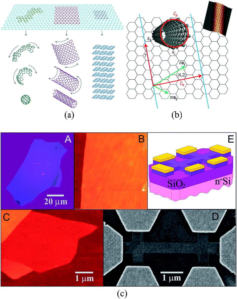 | ||
| Fig. 1 (a) The basic unit of the other C material – graphene.1 (b) The relational graph between graphene and carbon nanotubes.7 (c) Graphene film and devices (flow chart of graphene prepared by mechanical stripping method from A to E).3 | ||
Graphene comprises honeycomb-dimensional crystals closely arranged by sp2 hybridized carbon atoms, and hexagonal geometry makes graphene structure very stable.8 Each interlayer carbon atom bonds with the surrounding carbon atoms by sp2 hybridization, and contributes a non-bonding electron to form a large π bond, to allow the electrons to move freely between the layers.
Graphene is the thinnest and hardest nanomaterial,9 with a tensile strength of 125 GPa, an elastic modulus of 1.1 TPa, and a two-dimensional ultimate plane strength of 42 N m−2. Graphene's carrier mobility is 2 × 105 cm2 (V−1 s−1)10,11 and is only affected by impurities and defects. Graphene's thermal conductivity is up to 5.5 × 10³ W (m−1 K−1).12,13 Theoretically, graphene's specific surface area is up to 2630 m2 g−1. These unique physical properties make graphene to be widely applied in many areas of nanoelectronic devices, spin electronics, energy storage, and thermal conductivity materials.
The C![[double bond, length as m-dash]](https://www.rsc.org/images/entities/char_e001.gif) C covalent bond of carbon nanotubes makes the axial Young's modulus of carbon nanotubes reach as high as 5 TPa,20,23,24 while the length–diameter ratio is as high as 104, the comparison area is more than 1500 m2 g−1 (ref. 25 and 26) and the current carrying capacity is up to 109 A cm−2;27,28 One of the optical properties of carbon nanotubes is their wide band absorption.29,30 As a good thermal conductor, the axial thermal conductivity of CNTs is up to 6600 W (M−1 K−1), with excellent field emission characteristics, where its emission current mainly comes from the occupied states being slightly lower than the Fermi level.
C covalent bond of carbon nanotubes makes the axial Young's modulus of carbon nanotubes reach as high as 5 TPa,20,23,24 while the length–diameter ratio is as high as 104, the comparison area is more than 1500 m2 g−1 (ref. 25 and 26) and the current carrying capacity is up to 109 A cm−2;27,28 One of the optical properties of carbon nanotubes is their wide band absorption.29,30 As a good thermal conductor, the axial thermal conductivity of CNTs is up to 6600 W (M−1 K−1), with excellent field emission characteristics, where its emission current mainly comes from the occupied states being slightly lower than the Fermi level.
As representatives of one-dimensional and two-dimensional nanomaterials, while graphene is composed only by a single carbon atomic layer, this is the true sense of a the two-dimensional crystal structure. Compared with graphene, carbon nanotubes have a higher total amount of carbon atoms, making themselves have a lower energy of the edge dangling bonds than graphene, which can stabilize the molecules in the air without them reacting with the air. From a performance standpoint, graphene has similar or more excellent characteristics than carbon nanotubes in terms of conductivity, carrier mobility, thermal conductivity, free electron moving space, strength and stiffness.
Graphene and carbon-nanotubes have different applications for many reasons, but ultimately the differences can be attributed to the difference between one-dimensional materials and two-dimensional material. For example, a single carbon nanotube can be regarded as a single crystal with a high length–diameter ratio; however, the current synthesis and assembly technology cannot prepare the carbon nanotube crystals in a macroscopic scale, which limits their applications. While, an advantage of graphene is that it is a two-dimensional crystal structure, and its strength, conductivity and thermal conductivity are among the best of other two-dimensional crystal materials and it has a broad range of application prospects because of the ability of having a large area of continuous growth.
1.2 Introduction to graphene-like two-dimensional crystals – hexagonal boron nitride
Hexagonal boron nitride (h-BN),31 which belongs to a hexagonal system, is a white block or powder, has a layered structure similar to the graphene lattice constant and similar characteristics, and is sometimes referred to as ‘white graphene’.32–34 h-BN is a lattice alternately arranged by B atoms and N atoms in a two-dimensional plane by hexagonal lattice formation, showing a honeycomb structure (Fig. 2). The N atomic nucleus and B atom are combined by an sp2 orbital to form a strong σ bond,35–39 with the interlayer combined by weak van der Waals forces such that it can slide easily between the layers and has soft lubricating properties.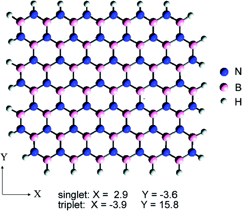 | ||
| Fig. 2 Flat structure diagram of h-BN. Blue on behalf of nitrogen atoms and pink on behalf of boron atoms, respectively.34 | ||
In 1995, Nagashima et al. used an epitaxial growth on a variety of metal surfaces to obtain h-BN crystals.40 A team from the University of Manchester adopted a micro-mechanical peeling method in 2005 to successfully prepare a two-dimensional h-BN.41 The band gap of h-BN is about 5.9 eV, while the Mohs' scale of hardness is about 2, the bulk modulus about 36.5 GP, the heat conductivity layer up to 600–1000 W m−1 K−1, the coefficient of thermal expansion layer about −2.7 × 10⁻⁶ per °C (interlayer about 30 × 10−6 per °C) and the refractive index about 1.8, and furthermore, it has neutron absorption ability.42–45 In addition, its anti-oxidation temperature is 900 °C and its thermos ability is up to 2000 °C, while at 2700 °C, in an inert environment it remains stable. Finally, h-BN also has good process ability, such as thermal shock resistance to electrical vibration, high resistance to break down the electric field strength, and is non-toxic and environmentally friendly, with no wettability to various metals or chemical corrosion and has other excellent physical and chemical properties, and consequently is widely used.46–53
1.3 Introduction of graphene/h-BN as a two-dimensional composite
Graphene has very good electronic properties. However, it will be a challenging to make graphene into nanoelectronic devices. Moreover, good mechanical stability is required when using scanning probe technology to detect micro-graphene.54 A substrate can be introduced to solve this problem, whereby, the introduction of the substrate can open up the graphene band gap, thereby improving the switching performance of graphene electronics.There have already been a lot studies into graphene and the substrate materials, such as Co,55 Ni,56–59 Ru60,61 and Pt,62,63 as well as semiconductors SiO2 (ref. 64–66) and SiC,67–69 which can be used as a substrate graphene. However, experiments show that the graphene on top of these substrates is very uneven, and it will have a lot of wrinkles, which could restrain the properties of graphene. For example, SiO2 is the most common graphene substrate, but on the SiO2 surface there are usually impurities, which can cause the scattering of charge or act as charge traps. Therefore, the growth and charge density distribution of graphene on the SiO2 substrate is very uneven (Fig. 3),70 which results in significant suppression of the carrier mobility of graphene. Recently, a lot of research studies have proven that hexagonal boron nitride is an ideal substrate and is ideally suited for graphene to maintain its geometrical and electrical properties.
 | ||
| Fig. 3 Comparison of the topography and charge density for graphene/BN vs. graphene/SiO2.73 | ||
Monolayer graphene and h-BN have a similar lattice structure, with a lattice mismatch of only about 1.5%.71 As a base, h-BN has a smooth surface without any charge traps, and it also has a low dielectric constant and high temperature stability as well as high thermal conductivity and other properties. With a dielectric constant ε of 3–4 and a breakdown electric field strength of about 0.7 V nm−1, h-BN is a great gate insulating layer for graphene. The surface optical phonon energy of h-BN is two orders of magnitude greater than that of SiO2, which indicates that using h-BN as the substrate is likely to improve the performance of graphene devices in conditions such as at higher temperature and in a higher electric field. In the h-BN single cell, the difference in grid energy between nitrogen atoms and boron atoms leads to a broad band gap of about 5.9 eV,72 which can help open the band gap of graphene. All the above show that h-BN is an ideal substrate material for graphene.
Dean et al., for the first time using h-BN as a supporting substrate of graphene, fabricated graphene transistors device with high mobility,72 on which a clear graphene quantum Hall effect was observed. Ponomarenko et al. (Fig. 3)73 used physical transfer to combine thin sheets of graphene and h-BN crystals to produce a heterojunction device with two single layers of graphene crystals. At the same time, researchers have succeeded in achieving a variety of graphene heterojunctions and superlattice structures with more complex structure;74–76 for instance, researchers in the UK and the US observed the novel Hofstadter Butterfly phenomenon on graphene/h-BN heterojunction devices, respectively.77,78 Since then, researchers have used a variety of methods to fabricate graphene/h-BN heterostructure functional devices, with the original purpose of improving the quality and speed of preparation of graphene instead of actually studying the performance of the graphene/h-BN heterostructures.
The single layer graphene and h-BN have similar lattice structure, and lattice mismatch is only about 1.5%.63 As a base, h-BN has smooth surface without charge trap, and it also has a low dielectric constant, high temperature stability as well as high thermal conductivity and other properties. Hexagonal boron nitride with dielectric constant ε of 3–4, breakdown electric field strength of about 0.7 V nm−1, is great gate insulating layer for graphene. The surface optical phonon energy of h-BN is two orders of magnitude greater than that of SiO2, which indicates that the using of hexagonal boron nitride as the substrate is likely to improve the performance of graphene device in conditions like high temperature and high electric field.17 In the h-BN single cell the difference of grid energy between nitrogen atoms and boron atoms leads to a broad band gap of about 5.9 eV,64 which can help open the band gap of graphene. All above shows that h-BN is an ideal substrate material for graphene.
2 Graphene
2.1 Structure of graphene
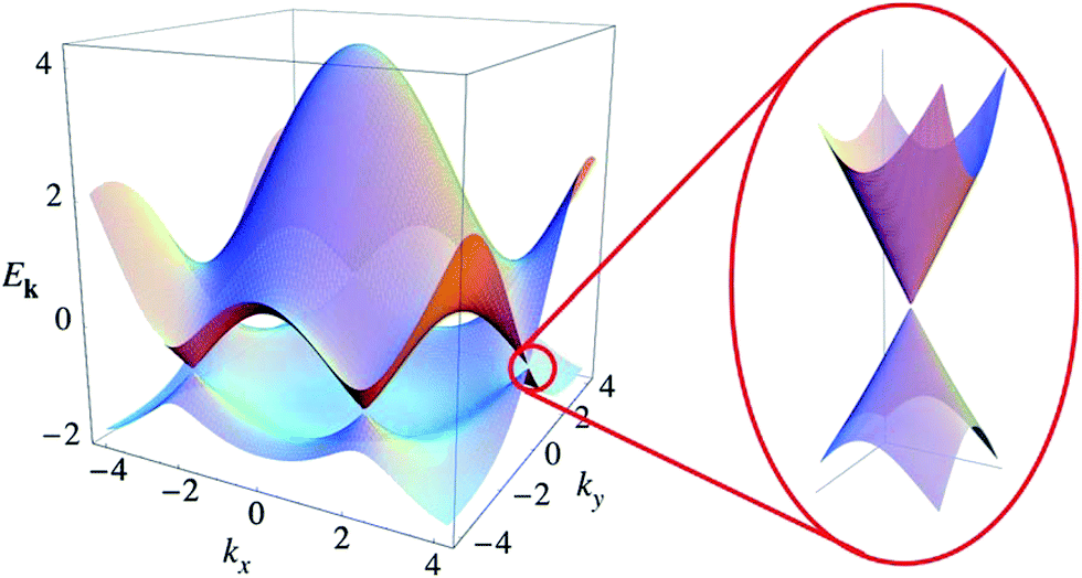
Ideal graphene is a single layer of two-dimensional atomic crystals with an orthohexagonal lattice structure. The length of the C–C bond is around 0.142 nm, and the thickness of the layer is 0.35 nm. In each state, a single carbon atom forms a strong σ bond with its three nearest neighbours, respectively, by sp2 orbital hybridization, causing occupied and unoccupied states to move away from each other. Each unit cell of graphene has two types of sub-lattice, type A and B (Fig. 4a), and there are chiral characteristics between the spins of electrons of A and B.79 | ||
| Fig. 4 (a) The relationship between distribution of A and B atoms in the unit cell of graphene. (b) Corresponding Brillouin zone. The Dirac cones are located at the K and M points.79 | ||
2.2 Preparation of graphene
The preparation of graphene can be classified into physical and chemical methods, including mechanical peeling1 and epitaxial growth,80 chemical cleavage,81 chemical vapour deposition (CVD),11 low thermal expansion,82 nanotubes cutting,83 metal catalysis and so on,84,85 as shown in Fig. 5. | ||
| Fig. 5 Several types of preparation methods of graphene (spectral analysis of graphene prepared by CVD method is shown from a to e in the left group figures. Sample image of graphene by epitaxial growth is shown from a to e in the middle of group figures. Epitaxial growth of graphene samples and their characteristics is shown from A to E in the right group figures).11,84,85 | ||
Yu et al. summarized the progress on the direct growth of graphene on semiconductor and insulator substrates in recent years.86Table 1 shows a comparison of the physical properties between several materials and h-BN as substrates.
| Al2O3 | SiO2 | Graphite | Graphite diamond | h-BN | ||
|---|---|---|---|---|---|---|
| Lattice constant | Face-centred: 1.27 | Orthogonal | a = 1.383 | a = 0.246 nm | 0.3567 | a = 0.2504 nm |
| b = 1.741 | ||||||
| c = 0.504 | c = 0.667 nm | c = 0.6661 nm | ||||
| Face-centred | 1.936 | |||||
| Thermal conductivity (W m−1 K−1) | 40 | 1.4 | 25–470 | 22 | 25.1 | |
| Dielectric constant | 6.8 | 3.9 | 8.7 | 5.7 | 4 | |
2.3 Physical properties of graphene
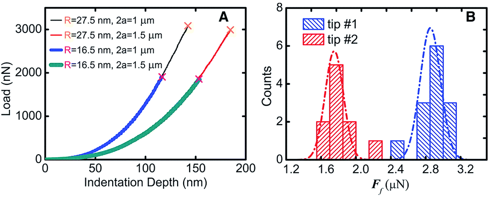 | ||
| Fig. 6 Fracture test results (A) the test line corresponding to different film diameters and tip radius. (B) Histogram and Gauss distribution of two kinds of fracture forces.9 | ||
Because of the high modulus of elasticity and the long mean free path of electrons, the thermal conductivity of graphene can reach up to 3000–6000 W m−1 K−1. Hong et al.11 showed that graphene's thermal conductivity was 5300 W m−1 K−1 but decreases as the temperature increases.12,89 Seol et al. studied graphene's thermal conductivity on a SiO2 substrate90 and the results showed that the value of thermal conductivity was still as high as 600 W m−1 K−1, even with the phenomenon of phonon scattering occurring due to the transfer of heat between the interface of the two materials. In addition, defects and the unordered arrangement of the edges will reduce the thermal conductivity of graphene (Fig. 7).91
 | ||
| Fig. 7 Different widths of graphene nanosheets' thermal conductivity changes at different temperatures ((a) The thermal conductivity change images of different materials at 300 K. (b) The anisotropy test images of different widths of nanoribbons at different temperatures).91 | ||
 | ||
| Fig. 8 Looking through one-atom-thick crystals.93 | ||
 | ||
| Fig. 9 Electronic dispersion in the honeycomb lattice.96 | ||
The unique band configuration of the Dirac point gives graphene excellent conductivity. Electrons in graphene pass through the barrier with 100% probability.96 Due to a strong force between the carbon atoms, the collision of carbon atoms has little effects on the motion of electrons. Chen et al., in 2008, by limitation of the external conditions found that the carrier mobility of graphene based on a SiO2 substrate could reach 4 × 104 cm2 V−1 s−1,64 which is comparable to the value of the best field-effect transistor, and at room temperature the carrier mobility of suspended graphene could reach up to 2 × 105 cm2 V−1 s−1, which is 140 times the value of silicon. Claire Biel et al. demonstrated that, in graphene, the mobility of electrons and holes are equal.82 The conductivity of graphene can reach 106 S m−1, which means it has the best conductivity among known materials at room temperature.
Meanwhile, graphene has a bipolar field-effect1 and the transmission characteristics of a ballistic.82 Through graphene atomic doping,97–99 control of the edge structure of graphene nano-strips,100 the imposing of an external electric field on the graphene and related materials,101 it is possible to regulate the size of the energy gap by adjusting the interaction between graphene and substrate materials.102–105
Wang et al. applied various annealing temperatures to oxidize graphene to regain its ferromagnetism at room temperature.110 Geim et al. obtained diamagnetic nano-graphene at room temperature and paramagnetic nano-graphene based on low temperature (Fig. 10).111 Two recent articles have pointed out that doped graphene under various conditions has paramagnetism.112
 | ||
| Fig. 10 Magnetic response of graphene ((a) Magnetic moment as a function of magnetic field intensity at different temperatures from 2 K to 300 K. (b) Magnetic moment images with the changing temperature for the same sample).111 | ||
2.4 Raman spectrum of graphene
In 2006, Ferrari et al. first proposed the Raman spectroscopy identification method for single-layer graphene (Fig. 11).113 The major Raman spectrum characteristic peak for graphene is the G peak, caused by in-layer transverse vibrations of sp2 hybridized carbon atoms, and this appears in the vicinity of 1580 cm−1. The peak can effectively reflect the number of layers of graphene sheets, and is vulnerable to stress. With the increase in the number of layers, N, the position of the G peak will move to lower frequency, and this displacement of the movement is related to 1/N.114 The G peak is susceptible to doping, and the peak frequency and peak width can be used to detect the doping level.115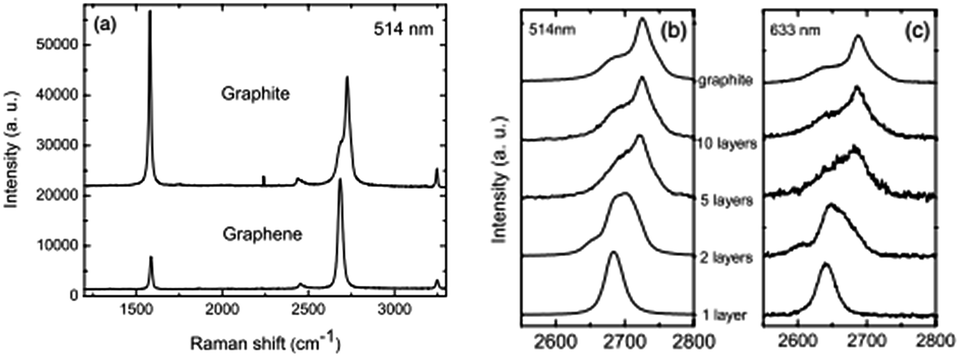 | ||
| Fig. 11 Raman spectra of ideal graphene and of different layers under different wavelengths.113 | ||
The D peak usually refers to a disordered vibration peak of graphene. The peak appears at 1270–1450 cm−1, with its specific location related to the excitation wavelength.116 The peak is caused by the lattice vibration of graphene keeping away from the centre of the Brillouin zone, and is used to characterize defects or the edge of the graphene sample. The 2D peak is a two-phonon resonance second-order Raman peak, while the double resonance process connection phonon wave vector and the electronic band makes the frequency of the 2D peak susceptible to excitation wavelength.117
Characteristic peaks can be used to determine the different layers of graphene, and, as an optical means of almost zero damage, Raman spectroscopy, which is widely recognized and used by researchers, has greatly enhanced the efficiency of this kind of identification.
3 Two-dimensional hexagonal boron nitride (h-BN)
3.1 Structure of h-BN
As an analogy of graphene, B atoms and N atoms of a 2D h-BN are alternately arranged to form a honeycomb structure, following the law of a hexagonal lattice formation (Fig. 12).118,119 The B–N bond length is 1.45 Å, which forms through sp2 hybridization. Three sp2 orbits of each B atom combine with the sp2 orbit of adjacent N atoms to form a strong σ bond, likewise, three sp2 orbits of each N atom combine with the sp2 orbit of adjacent B atoms to form a strong σ bond. Adjacent layers of h-BN are combined with weak van der Waals forces, and in each layer B atoms and N atoms are joined by covalent bonds. The interlayer spacing of graphene is 0.335 nm, and the interlayer spacing of h-BN is 0.333 nm, which is slightly less than that of the graphite. In the c-axis direction of h-BN, the bonding force is small and the interlayer spacing is large, making the interlayer slide easily.120–134 | ||
| Fig. 12 Structure of h-BN. (A) Stereogram. (B) The 2D floor plan.118 | ||
3.2 Preparation of h-BN
Whether by experimental or theoretical considerations, h-BN crystals have been prepared in many ways.40,133–143 Some basic methods include: mechanical separation,38 chemical vapour deposition (CVD),133,134 aqueous solvent thermal synthesis,135–137 solvent stripping and so on (Fig. 13).129,138 | ||
| Fig. 13 Preparation methods of h-BN with the mechanical stripping method and the CVD method (The left group figures: (a) low magnification and large defocus of the h-BN TEM images. (b) The folding images for h-BN. The right group figures: (a) Photograph of a large h-BN film on a silicon substrate. Scale bar is 1 cm. (b), SEM image shows a h-BN film (scale bar 10 μm). (c and d) AFM image and line-scan profile indicate that h-BN film has uniform thickness of a 1 nm. Scale bar is 2 μm).38,133 | ||
3.3 Physical properties of h-BN
 | ||
| Fig. 14 Orbital property and electronic structure of h-BN.118 | ||
 | ||
| Fig. 15 Schematic of nanoindentation on a suspended h-BN membrane.133 | ||
At room temperature, the thermal conductivity of h-BN is up to 400 W m−1 K−1, which is higher than the majority of metals and ceramic materials. h-BN has a typical anisotropy: having a high thermal conductivity in the direction perpendicular to the c-axis of 300 W (m−1 K−1), low thermal expansion coefficient of 0–2.6 × 10⁻⁴ K−1, and a relatively high tensile strength (41 MPa). When parallel to the c-axis direction, h-BN has a lower thermal conductivity of 20–30 W (m−1 K−1) and high compressive strength, and so on.138,142–145
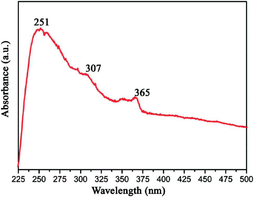
Gao et al. measured the UV-vis optical absorption spectrum of h-BN by investigating as-prepared h-BN nanosheets. From Fig. 16, we can see that the absorption peaks around 251, 307 and 365 nm corresponds to a band gap energy of 4.94, 4.04, and 3.40 eV, respectively. These two absorption peaks at 307 and 365 nm are due to the optical transitions and the redistribution of h-BN's electron–hole density between van Hove singularities of excited state.131 As a wide band gap material,35,146 h-BN is transparent in infrared and visible light, while in ultraviolet light it has a strong optical absorption at 251 nm with a strong exciton peak.131
 | ||
| Fig. 16 UV-vis optical absorption spectra of BN.131 | ||
 | ||
| Fig. 17 Calculated band structures of the pristine graphitic–BN with different atoms. (a) with a boron atom (b) and a nitrogen atom (c) substituted by a carbon atom.148 | ||
By researching no passivation and passivation with zigzag boron nitride nano-ribbons, Lai et al. found that its system presents as semi-metallic,150 while the nitrogen atom edge passivation is not magnetic. V. Barone et al. found no spontaneous spin polarization in passivated serrated boron nitride nano-ribbons,146 while under the effect of an external electric field, the material can realize a metal-semiconductor-semimetal transition. F. W. Zheng et al. found that when the B atoms are edge passivated,151 the electronic polarization rate at the Fermi level is 100%, showing semi-metallic properties with a band gap of 0.38 eV, while the conductivity of the system is decided by metallic spin electrons. Also, when the N atoms are edge passivated, the antiferromagnetic structure is more stable than the ferromagnetic structure, as the energy of the former is approximately 33 meV per (edge atom) more than that of the latter.
3.4 Raman spectroscopy of h-BN
The Raman characteristic peaks of h-BN crystals is at about 1366 cm−1, and a single-layer peak will blue-shift 4 cm−1 due to the BN bond of a single-layer h-BN having slightly shorter phonon modes, causing E2g to harden (Fig. 18).152 The red-shift depends on random strain introduced by the stripping process, which dominates in the double h-BN. Therefore, the h-BN Raman characteristic peak is red-shift 1–2 cm−1. | ||
| Fig. 18 Raman spectra of 2D h-BN.152 | ||
4 Composite structure of graphene/h-BN
4.1 Research into graphene/h-BN heterojunction structures
The linear dispersion relationship of graphene near the Dirac point is responsible for its high carrier mobility characteristic, which has attracted wide attention (Fig. 19)70 and is considered an important characteristic for electronic devices utilizing carbon Keener materials.106,153,154 However, its zero band gap has hindered graphene's application in the construction of nanoelectronic devices, because these devices require a valid strip gap. Thus, whether graphene can open an effective band gap becomes critical. Researchers have used a variety of methods to achieve this objective. For example, hydrogenated graphene,155 isoelectronic co-doping of B and N atoms,156 adsorption of metal atoms,157 double extra electric field components,2,158 a graphene–substrate interaction,159 the level of the tensile stress and so on.71 All the methods were double nanostructures, which makes them exceptionally compelling, because the interaction between the layers and stacking mode provides an additional degree of freedom to regulate the electronic structure. C materials and h-BN have matched lattice constants. By forming a graphene/h-BN heterostructure to regulate graphene's electronic structure and energy band, the goal of applying graphene to optoelectronic devices is achieved. | ||
| Fig. 19 STM pictures of graphene/h-BN heterostructure with different rotational orientations.70 | ||
In 2000, Oshima et al.160 prepared two-layer structured graphene/h-BN in the Ni(111) direction, and studied the influence of monolayer graphene on the Ni(111) substrate grown h-BN single-layer electronic structure, ignoring the effects of h-BN on the electronic structure of graphene. Stewart et al. calculated the most stable configuration of graphene/h-BN electronic properties through the tight-binding and density functional theory.161 Their research showed that a level perpendicular to the applied electric field could regulate the electronic structure of the whole system, including the offset, anti-cross, and other forms of energy deformation, and could be used to control the size of the band gap according to different needs. In 2010, Bjelkevig et al. used the CVD method on Ru's (0001) direction to prepare a double heterojunction structure graphene/h-BN.162 The study found that there was a strong charge transfer between the BN and graphene, which occupied part of the π* band, and made the occupied σ* closer to the Fermi level. This showed that forming a double heterojunction structure of graphene/h-BN could regulate the electronic structure of graphene. In 2012, Tang et al. made single-crystal graphene grow on h-BN,163 although the growth size was not large, and then used Raman technology to demonstrate that the nucleation growth of hexagonal graphene involved a single crystal structure. This finding enriched the means of preparing graphene boron nitride heterojunctions, and makes the rapid preparation of high-quality graphene/h-BN possible. Especially recently, Tang et al. used the CVD method to make graphene from graphene/h-BN in an efficient large area,164 such that the preparation of graphene reached a new level. Meanwhile, the applications of graphene/h-BN heterostructures in nanodevices has gained technical support.
4.2 Composite mode structure of graphene/h-BN
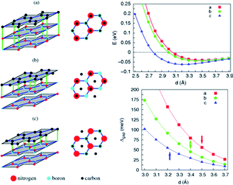
Zhong et al. verified that the AB stacking of the graphene/h-BN double-layer heterogeneous nanostructure was the most stable by first-principles calculations, and found that as stress increases, the band gap increases linearly.165 Fan et al. applied LDA and PBE + VDW methods to study the structural energy variations of the graphene/h-BN double-layer heterogeneous nanostructures of four stacking patterns with various interlayer distances.166 The results showed that with either method, AB stacking, where N atoms are positioned towards the centre of the graphene hexagon and B atoms are positioned towards the C atoms, is most stable at various interlayer distances, with the stable model and calculation results shown in Fig. 20. They studied four kinds of stacking configurations: I–IV. I had a hexagonal configuration (AA), where C atoms are positioned above the B atoms or N atoms. II and III had a Bernal configuration (AB), where C atoms of one sub-lattice of graphene are positioned above the N atoms (configuration II) or B atoms (configuration III), while C atoms of the other sub-lattice of graphene are positioned above the centre of the BN hexagon. Configuration IV can be obtained from the translation of the h-BN layer in configuration I along the direction of the C–C bonds by the distance of 1/6 graphene lattice constant.166 Kan et al. also found that the band gap of the graphene/h-BN double-layer heterogeneous AB stacking stable structure could be modulated through the interlayer distances by first principles.167
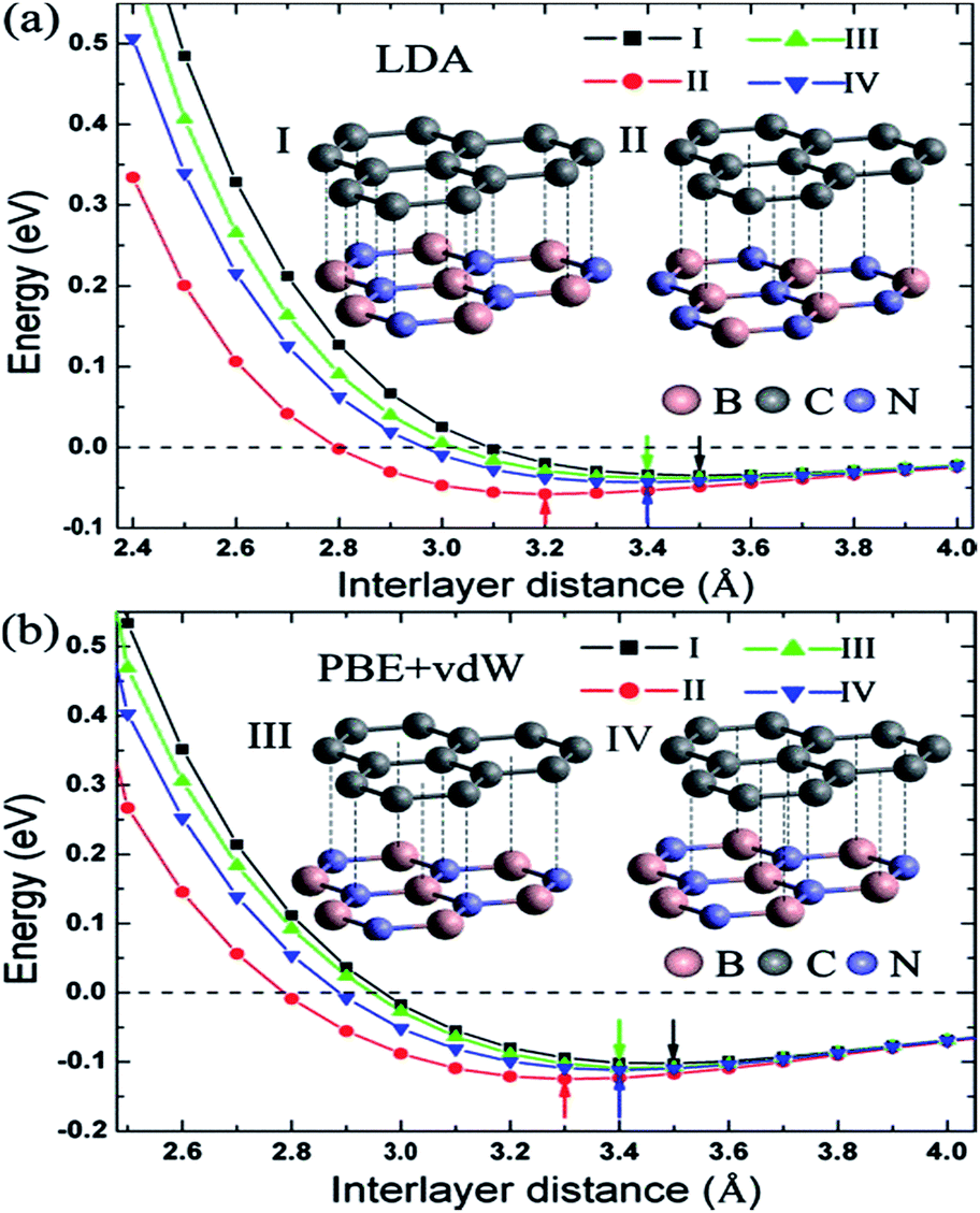 | ||
| Fig. 20 BE per unit cell of graphene/h-BN with different stacking manners.166 | ||
Utilizing the VASP package local density approximation (LDA), the changes of binding energy (BE) for each original cell with the variations of the interlayer distance were calculated,168 and the results showed that various stacking structures had different equilibrium positions, specifically, different structure balancing interlayer spacing of 3.5, 3.2, 3.4 and 3.4 Å for configurations I–IV, respectively, which were consistent with previous calculations for the deposition of graphene on boron nitride.71 For this double-layer heterostructure, the order of stability under the same interlayer spacing was: configuration I < configuration III < configuration IV < configuration II. This phenomenon is related to the attractive interaction between the electrons in graphene and the cations in BN and to the repulsive interaction between the electrons in graphene and the anions in BN; while N anions tend to be directly above the centre of the C hexagon, because the electron density of this position is low, and B cations tend to be directly above C atoms to enhance the effect of attracting (configuration II).
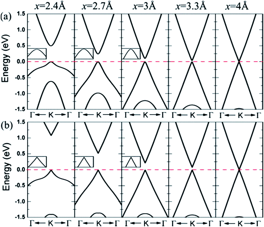 | ||
| Fig. 21 Band lines near the Fermi level of C/BN HBLs with interlayer distances x = 5, 3.3, 3, 2.7, and 2.4 Å for (a) configuration II and (b) configuration IV. The Fermi level is set to zero.166 | ||
When the interlayer distance is large enough, the energy band structure near the Fermi level is consistent with that of monolayer graphene, because the interlayer interaction under such a distance is very weak. With the decrease of the distance between the layers, the interlayer interaction increases, resulting in a reconstruction of HBL's charge. Due to the different chemical environments, the equivalence between the two different sub-lattice of graphene is destroyed, and a small band gap is opened up at the Dirac point between the valence and conduction bands. Obviously, the smaller the interlayer distance, the bigger the opened band gap, which thus provides a possible approach for the band gap regulation of graphene.
For HBLs of configuration I–III, at the Dirac point, there is a parabolic dispersion relationship (nearly free electrons) between the valence and conduction band near the Fermi level, which means the effective mass of electrons is non-zero. However, for HBLs of configuration IV, a band gap is opened near the Dirac point, and the energy band structure maintains the linear dispersion relationship with graphene, which means the effective mass of electrons and holes is zero. The high mobility of carriers in this heterogeneous double layer, of which the band gap is not zero, is comparable to that in the graphene monolayer, which is significant for the preparation of graphene devices that require both a band gap and high carrier mobility.
The variation of the band gap of the HBLs can be studied by adjusting the interlayer distance, as shown in Fig. 22.167 The band gap increases progressively with the decrease of the interlayer distance, but the extent of change is different for the four configurations. Under the same interlayer distance, configuration I and II have the maximum and minimum band gap, respectively, and the other two configurations have the medium band gap.
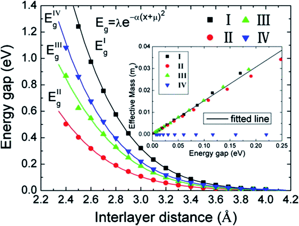 | ||
| Fig. 22 Variation in the energy gap of HBLs as a function of interlayer spacing. The inset shows the variation of the effective masses vs. the band gap.166 | ||
From Fig. 23, we can see that the charge density near the two sub-lattice of graphene is no longer equivalent, and as the interlayer distance decreases, this asymmetry becomes more pronounced. This shows that when the interlayer distance is compressed, the difference between the potential energy of the two sub-lattices of graphene becomes larger. Furthermore, for the four configurations, the degree of sensitivity to the change of the interlayer distance is related to the atomic arrangement of the HBLs. The carbon atom of configuration I is exactly located above the B atom or N atom of the BN monolayer, causing the highest asymmetry of the two graphene sub-lattices, and therefore configuration I is the most sensitive to the interlayer distance. The C atoms of one sub-lattice of configuration I are located directly above the B atoms; however, all the C atoms are symmetrically distributed around the N atoms. In this arrangement, the asymmetry of the two carbon atoms sub-lattice is the lowest, so configuration II is the least sensitive to the interlayer distance. This is also consistent with the trends in charge density with the variation of interlayer distance for the four configurations, as shown in Fig. 23(b).
 | ||
| Fig. 23 Contour plots of the charge density difference (a) for stacking pattern I at the interlayer distances x = 2.7, 3.2, 4 and 5 Å, respectively, and (b) for the four stacking patterns (I–IV) at the interlayer distance x = 3 Å.198 | ||
DFT calculations show that for the graphene/h-BN HBLs, the band gap and effective mass of carriers can be regulated by changing the interlayer distance and stacking patterns. With the decrease of the interlayer distance, the band gap gradually increases. With the increase of the band gap, for AA and AB stacking patterns (configurations I–III), the effective mass of carriers linearly increases; for configuration IV, the linear dispersion relation in the monolayer graphene reserves in graphene/h-BN HBLs. The quality of controllable band gap and the small effective mass (even zero for configuration IV) of C/BN HBLs support it having potential important applications in the construction of high-performance graphene nanodevices.
4.3 Preparations of graphene/h-BN heterostructures
From 2010 to today, the methods of preparing graphene/h-BN heterostructures have become a hot topic of research and more and more reliable methods have been developed.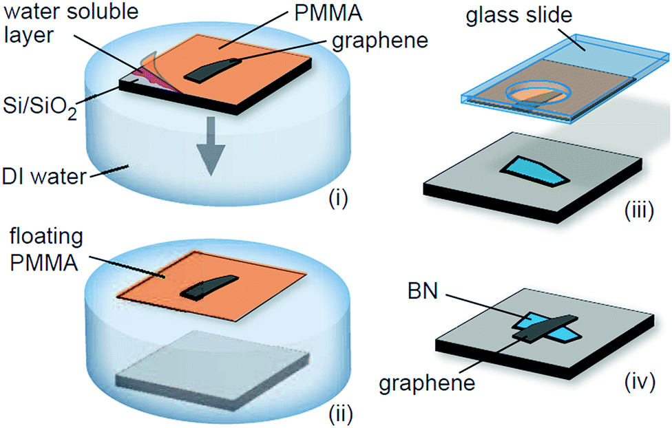 | ||
| Fig. 24 Schematic of the transfer process to fabricate graphene-on-BN devices.72 | ||
 | ||
| Fig. 25 Schematic of the liquid phase exfoliating method.(a) The illustration of the stacked structure of graphene and h-BN nanosheets. (b)–(d) The TEM images of stack structure with different resolutions. (e) Graphene, h-BN and BNG hybrid free standing films. (f) The h-BN/GTEM image for mapping. (g) Boron mapping of image (f). (h) EELS spectrum of h-BN/graphene hybrid, K-shell excitations of B, C, and N.169 | ||
These two methods inevitably have impurities appear on the top and bottom of the graphene, a low success rate of the lattice corresponding paste, poor precision, and the product is easy to fold. In the preparation of this method, the larger the boron nitride, the higher the preparation success rate; the larger the graphene, the easier the device preparation, which is tough in the mechanical stripping process.
 | ||
| Fig. 26 Dry preparation of graphene/h-BN as a schematic and sample image: (a) schematic of the transfer mask. (b) SLG and BLG areas on the mask, the scale bar equals 5 μm. (c) Graphene alignment and transfer to a h-BN crystal. (d) Graphene flake in a Hall bar geometry on h-BN.170 | ||
W. Gannett et al. prepared a graphene/h-BN heterojunction by using CVD and run appropriate tests in 2011. After that, many researchers gradually improved the preparation method and made the heterostructure grow faster and faster, with the quality also getting better and better (Fig. 27).176
 | ||
| Fig. 27 (a)–(d) Sample fabrication steps shown schematically. (e) SEM image of graphene on a candidate h-BN flake. (f) Optical image of a finished graphene-on-BN device, with the electrodes labelled and the graphene outlined.176 | ||
Liu et al. realized the superposed growth of graphene and h-BN by a two-step gas-phase process.177 Subsequently, Yan et al. used PMMA as a solid carbon source to achieve the growth of bilayer graphene on a chemically vapour-grown h-BN substrate.178 Tang et al.,179,180 used methane as gaseous carbon source on a h-BN substrate to achieve graphene lamellar nucleation growth with a superlattice structure.164 Recently, Kim et al. synthesized graphene/h-BN heterostructures with different hybridization modes by modifying the vapour-phase growth process.174 In 2016, Song et al. used PMMA particles to control the nucleation density and grain size, which provides the technical direction for the high-quality mass production of graphene/h-BN.181
 | ||
| Fig. 28 LEED and STM dI/dV data for BN monolayer and graphene/h-BN heterojunction grown on Ru(0001).162 | ||
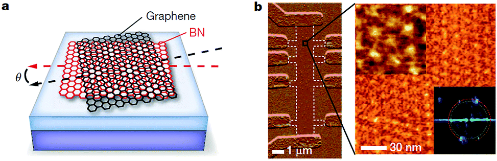 | ||
| Fig. 29 Moire' superlattice of graphene/h-BN. (a) The schematic diagram of moiré pattern for graphene on h-BN. (b) AFM image of a multiterminal Hall bar and a high-resolution image of a magnified region.185 | ||
The physical transfer method can realize the transfer of graphene on the surface of h-BN. However, this technique also brings issues of structural inhomogeneity and interfacial contamination. Now, researchers are exploring further optimized methods.
 | ||
| Fig. 30 The method of epitaxial graphene growth and the AFM image.187 | ||
 | ||
| Fig. 31 Growth of graphene/h-BN-stacked heterostructures: schematic illustration and optical images of the as-grown sample on the growth substrates.188 | ||
4.4 Properties of graphene/h-BN heterostructures
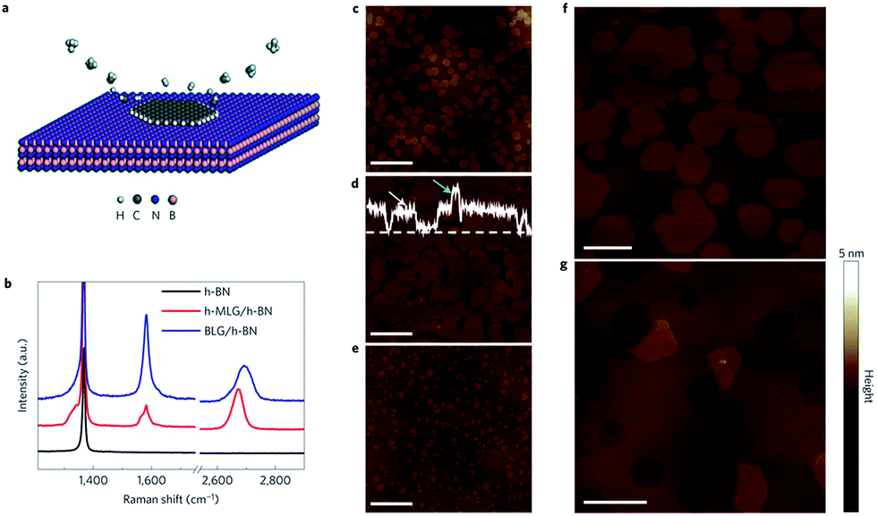
Graphene/h-BN heterostructures have attracted much attention because of their novel electrical, morphological, optoelectronics, mechanical and thermal properties.Yang et al.192 experimentally studied the imaging properties, such as the phonon spectrum of the far-field and near-field of graphene/h-BN heterostructures and photon polarization and polarization (Fig. 32); they also compared graphene excitation characteristics based on different substrates. The experimental results showed that the h-BN substrate has small inhibition on the photoelectric characteristics of graphene, and that h-BN as a graphene substrate has almost no effect on the optical properties of graphene.
 | ||
| Fig. 32 The coupling mechanism of graphene plasmons and the h-BN optical phonons. (a) The schematic diagram of Graphene plasmon and h-BN o-TO phonon. (b) Plasmon frequencies as a function of wave vector for different hybridized mode peaks. (c) Line profile of s-SNOM optical signals at the excitation wavelength of 970 cm−1. (d) s-SNOM images from 2D scan of the tip position near the graphene edge with varied excitation wavelengths.192 | ||
| Material | Crystal structure | Nearest neighbour distance (nm) | Lattice parameters (nm) | Inter-layer spacing (nm) |
|---|---|---|---|---|
| h-BN | Hexagonal | 0.144 | a: 0.250 | 0.333 |
| c: 0.666 | ||||
| Graphite | Hexagonal | 0.142 | a: 0.246 | 0.335 |
| c: 0.670 |
In several experimental preparations of graphene/h-BN, the lattice constants of graphene and h-BN had a 1.84% difference, and there is a certain angle of rotation between the two hexagonal holes sheet layers, making graphene/h-BN heterostructures form Murray stripes (Fig. 33).70,195 This formation of superlattice, results in a lot of new properties, in addition to the zero band gap, Fermi velocity changes, states of jitter of the local density and the superlattice features of the local charge density.196
 | ||
| Fig. 33 Real space and Fourier transforms of Moiré patterns with different ratio in (a) and (b).195 | ||
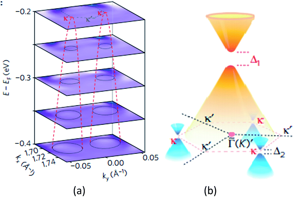
Giovannetti et al.,71 in 2007, proposed the introduction of a band gap (Fig. 34) by depositing the monolayer graphene on a h-BN substrate. With a different stacked manner, the graphene/h-BN heterostructure's band gap varied, and different distances of the layers generated a variation in the band gap. Hüser et al.,197 by calculations, obtained the electronic properties of graphene/h-BN heterostructures, and found that in the band, some small band gap can be opened. Wang et al.198 used angular resolution electron spectroscopy, for the first time, to directly measure original and second-level best Dirac band structures (Fig. 35) of a graphene/h-BN heterostructure, and in the original and second-level Dirac cone found up to 100 and 160 meV energy gaps, respectively, which revealed the importance of space inversion symmetry in a heterogeneous structure and the band modulation capacity of the van der Waals heterostructure.
 | ||
| Fig. 34 The three inequivalent orientations of single-layer graphene on a h-BN surface and the total energy E of graphene on a h-BN surface for the three manners.71 | ||
 | ||
| Fig. 35 (a) Stacking of constant-energy maps of EDC curvature to show the conical dispersion at the two κ points. d1–d5, dispersions along the cuts d1–d5 shown in a1. The white dashed lines are guides for the evolution of the SDCs dispersions. The black arrow indicates the dispersion from the original Dirac cone. (b) Schematic drawing of the band structure in the graphene/h-BN heterostructure, showing the gapped original Dirac point with gapped SDPs at three out of six corners of the SBZ (κ points).198 | ||
Ding et al.,203 in 2011, specifically studied the magnetic properties of graphene/h-BN composites, particularly for abnormal paramagnetic behaviour of the graphene/h-BN composites at low temperature. They proposed an analysis of the low-temperature magnetization curve, and found that the paramagnetic parts (<20 K) were mainly from the point defects in the sample, and that the angular momentum quantum number J = 1/2. This was the first time that they theoretically explained why J = l/2, and also the first to give J = 1/2 in a graphene system. To study the low-temperature magnetization curve anomalies paramagnetic behaviour (20–50 K), they used several theoretical models to explain this phenomenon, such as the RKKY interaction in the antiferromagnetic spin-glass state, and in the itinerant electron paramagnetic strengthening effect. The experimental results and antiferromagnetic spin-glass theory have a degree of conflict, and only the itinerant electron paramagnetic strengthen theory can be consistent with all of their results. So they speculated that the abnormal paramagnetic behaviour of the graphene/h-BN system at low temperature (20–50 K) came from the paramagnetic strengthening effect generated by the itinerant electrons from the graphene and h-BN interface or near the interface between (Fig. 36).
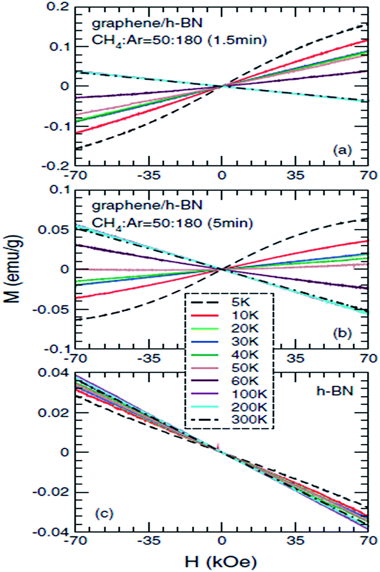 | ||
| Fig. 36 The measured mass magnetization Mas functions of magnetic fields H for (a) gra/h-BN sample 1, (b) gra/h-BN sample 2, and (c) h-BN substrate, at different temperatures T = 5, 10, 20, 30, 40, 50, 60, 100, 200, and 300 K.203 | ||
4.5 Potential applications of graphene/h-BN heterostructures
The introduction of h-BN as a substrate is to solve the graphene in traditional silicon material strain are imposed on the substrate and doping adverse problems. At the same time, formation of a van der Waals' heterostructure of graphene/h-BN increases the mobility of graphene and facilitates making nanometre functional devices, with wide potential application and practical significance.![[thin space (1/6-em)]](https://www.rsc.org/images/entities/char_2009.gif) 000 cm2 V−1 s−1, which was more than three times the mobility of graphene, similar to the calculation method for the SiO2 substrate, while the uniformity of charge was less than 7 × 1010 cm−2, three times smaller than silica basal graphene at room temperature. When the temperature was 15 K, the uniformity of charge was 1 × 109 cm−2, which was similar to suspended graphene. In addition to being an order of magnitude higher than that of the other test results, the roughness, intrinsic doping level, and chemical reactivity were lower.
000 cm2 V−1 s−1, which was more than three times the mobility of graphene, similar to the calculation method for the SiO2 substrate, while the uniformity of charge was less than 7 × 1010 cm−2, three times smaller than silica basal graphene at room temperature. When the temperature was 15 K, the uniformity of charge was 1 × 109 cm−2, which was similar to suspended graphene. In addition to being an order of magnitude higher than that of the other test results, the roughness, intrinsic doping level, and chemical reactivity were lower.
 | ||
| Fig. 37 Graphene/h-BN devices and the test chart. (a) AFM image of graphene/h-BN heterostructure. (b) Histogram of the height distribution measured by AFM for graphene, h-BN and SiO2. Resistance versus applied gate voltage for monolayer graphene (c) and bilayer graphene (d) on h-BN.204 | ||
From then on, more and more similar work was carried out; for instance, in 2011, Decker et al.;70 in 2013 and 2014, Lee et al.;205,206 also in 2014, Iqbal et al.;207 and in 2015, Song et al.;181 prepared a FET with graphene/h-BN, which obtained satisfactory results. All of the above, paid witness to the progress of graphene/h-BN van der Waals heterostructures for nanoelectronics applications.
 | ||
| Fig. 38 Schematic of a field-effect tunnelling transistor (A) and (B) tunnelling characteristics for a graphene/h-BN device with 6 ± 1 layers of h-BN as the tunnel barrier.182 | ||
 | ||
| Fig. 39 Schematic and test results of the device.209 | ||
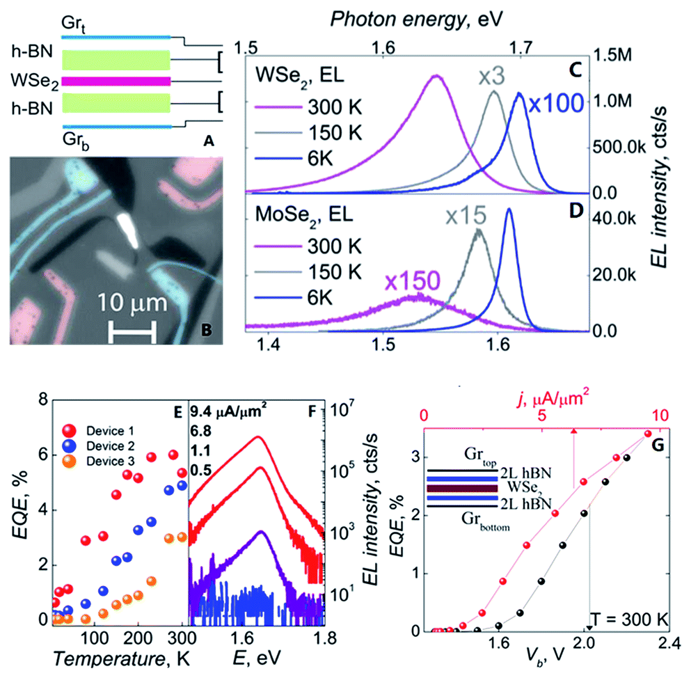 | ||
| Fig. 40 The flow and test figure of an LED.((A) Schematic of the device architecture. (B) Magnification monochrome image of WSe2 LEQW device. The change of photon energy under different temperature curve for WSe2 in (C) and MoSe2 in (D). (E) The image of quantum efficiency corresponding to temperature of three LED devices based WSe2. (F) Individual electroluminescence spectra plotted for four different injection current densities for a sample device. (G) The external quantum efficiency plotted against bias voltage and injection current density at T = 300 K for the same sample device in (F)).210 | ||
Wang et al.211 prepared graphene/h-BN van der Waals light-emitting diodes in 2015. In the two experiments, the heterostructures were made into LEDs, which provides direction for the preparation of nano-optoelectronic devices.
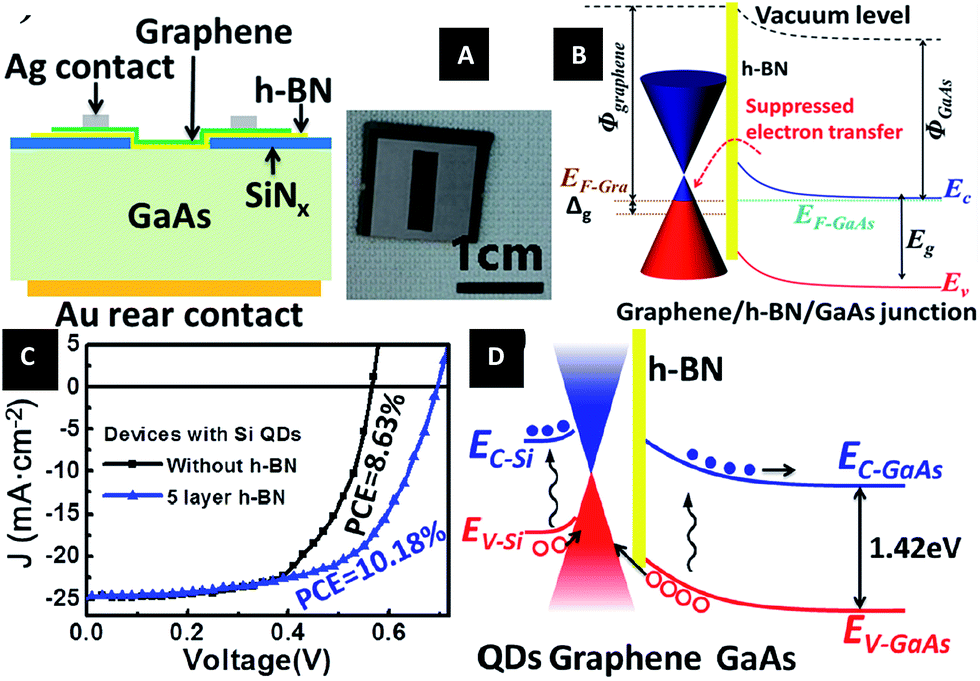 | ||
| Fig. 41 Graphene/h-BN/GaAs sandwich diode as a solar cell and photodetector. (A) Schematic of the graphene/h-BN/GaAs sandwich device. (B) Electronic band structure of graphene/h-BN/GaAs heterostructure. (C) J–V curves of solar cells based on graphene/GaAs and graphene/h-BN/GaAs heterostructure with Si QDs introduced photo-induced doping. (D) Electronic band structure of the graphene/h-BN/GaAs solar cell with Si QDs covering on graphene under illumination.212 | ||
 | ||
| Fig. 42 Schematic of the structures of: (A) an in-plane pressure sensor and (B) a tunnelling pressure sensor. Transmission spectra of: (C) the in-plane sensor and (D) the tunnelling sensor as functions of electron energy with different external pressure.213 | ||
Combining boron nitride with graphene offers multi-dimensional application opportunities in many fields: from the perspective of transport doping, from both horizontal and vertical components. People can conduct researches on physic based on boron nitride excellent substrate effect, and also can do researches on electronics to use boron nitride wide band gap. Therefore, there is still a hope to see good research into the aspects of mixing graphite and boron nitride.
5 Summaries and outlook
For logic devices of graphene/h-BN heterostructures, although a lot of theories and experiments prove that graphene based on h-BN has excellent optical characteristics, because of the zero band-gap properties of graphene, it is difficult to prepare a high-performance logic circuit as a direct field-effect transistor. Therefore, the band of 2D carbon-based material has a very important role in the regulation of optoelectronic device applications. For example, continuous research of graphene/h-BN heterostructures in the far infrared, the visible region and in the ultraviolet region can provide a basis for the preparation of applications of photovoltaic devices. Accounting for the different absorptions of graphene and h-BN in light regions, it is certain that a composite system of graphene/h-BN heterostructures has great use in the visible region, such as photoluminescence. On the other hand, regulation of the energy band engineering can be achieved by designing 2D heterostructure materials in combination with dielectric shielding. How the graphene layer of the graphene/h-BN heterostructure and the h-BN layer are bonded, and what is the force between the electrons will be revealed in the future. We believe that practical applications of heterostructure graphene/h-BN will greatly expand because of the unique optoelectronic properties of this structure.For graphene, due to its characteristics it is useful for optoelectronic devices, energy storage, and other aspects of mechanical reinforcement, and in line with its potential, the basic applied research in new 2D materials based on graphene has made great progress. When combined with other new 2D materials, by using 2D layered materials with different chemical bonds and the formation of different physical and chemical properties of new lattice structures, it should have even greater applications. For example: biomedical devices, photodetectors, chemical catalysis, clean energy generation and storage, surface-enhanced Raman scattering and so on.
Perhaps one of the most meaningful aspects of the research into graphene is that graphene has caused researchers to explore other 2D materials, which is a break from the long-term norm of studying 3D materials. At least in the history of science in materials, before graphene occurred, there was no one focusing on studying 2D materials. Therefore, the heuristic value of graphene is far greater than just the value of its own excellent performance. For instance, by combining the same or similar 2D structures of several different materials, the resulting new composite material have a lot of new characteristics that are exciting the scientific community, and hence the occurrence of 2D composite materials can help make the properties of the new materials more diversified.
Acknowledgements
This work was supported by National Natural Science Foundation of China (Grant No. 11374353, 91436102 and 11274149), National Basic Research Program of China (Grant number 2016YFA02008000), and the Program of Liaoning Key Laboratory of Semiconductor Light Emitting and Photocatalytic Materials.References
- A. K. Geim and K. S. Novoselov, Nat. Mater., 2007, 6, 183–191 CrossRef CAS PubMed.
- T. Ohta, A. Bostwick, T. Seyller, K. Horn and E. Rotenberg, Science, 2006, 313, 951–954 CrossRef CAS PubMed.
- K. S. Novoselov, A. K. Geim, S. V. Morozov, D. Jiang, Y. Zhang, S. V. Dubonos, I. V. Grigorieva and A. A. Firsov, Science, 2004, 306, 666–669 CrossRef CAS PubMed.
- J. Chen, Nature, 2012, 487, 77–81 CrossRef CAS PubMed.
- X. Geng, L. Niu, Z. Xing, R. Song, G. Liu, M. Sun, G. Cheng, H. Zhong, Z. Liu and Z. Zhang, Adv. Mater., 2010, 22, 638–642 CrossRef CAS PubMed.
- A. K. Geim, Angew. Chem., 2011, 50, 6966–6985 CrossRef CAS.
- R. Dagani, Nat. Nanotechnol., 2007, 2, 605–615 CrossRef.
- Y. B. Tang, C. S. Lee, Z. H. Chen, G. D. Yuan, Z. H. Kang, L. B. Luo, H. S. Song, Y. Liu, Z. B. He and W. J. Zhang, Nano Lett., 2009, 9, 1374–1377 CrossRef CAS.
- C. Lee, X. Wei, J. W. Kysar and J. Hone, Science, 2008, 321, 385–388 CrossRef CAS PubMed.
- K. I. Bolotin, K. J. Sikes, Z. Jiang, M. Klima, G. Fudenberg, J. Hone, P. Kim and H. L. Stormer, Solid State Commun., 2008, 146, 351–355 CrossRef CAS.
- B. H. Hong, Nature, 2009, 457, 706–710 CrossRef.
- A. A. Balandin, Nat. Mater., 2011, 10, 569–581 CrossRef CAS.
- L. A. Falkovsky, Phys. Lett. A, 2008, 372, 5189–5192 CrossRef CAS.
- S. Iijima, Nature, 1991, 354, 56–58 CrossRef CAS.
- D. S. Bethune, C. H. Klang, M. S. D. Vries, G. Gorman, R. Savoy, J. Vazquez and R. Beyers, Nature, 1993, 363, 605–607 CrossRef CAS.
- S. Iijima and T. Ichihashi, Nature, 1993, 364, 603–605 CrossRef CAS.
- L. Guan, Nano Lett., 2008, 8, 459–462 CrossRef CAS PubMed.
- Q. Wen, R. Zhang, W. Qian, Y. Wang, P. Tan, J. Nie and F. Wei, Chem. Mater., 2010, 22, 1294–1296 CrossRef CAS.
- S. Iijima, P. M. Ajayan and T. Ichihashi, Phys. Rev. Lett., 1992, 69, 3100–3103 CrossRef CAS PubMed.
- D. Galpaya, M. Wang, G. George and N. Motta, J. Appl. Phys., 2001, 116, 053510–053518 Search PubMed.
- R. Saito, M. Fujita, G. Dresselhaus and M. S. Dresselhaus, Appl. Phys. Lett., 1992, 60, 2204–2206 CrossRef CAS.
- N. Hamada, S. Sawada and A. Oshiyama, Phys. Rev. Lett., 1992, 68, 1579–1581 CrossRef CAS.
- M. M. J. Treacy, T. W. Ebbesen and J. M. Gibson, Nature, 1996, 381, 678–680 CrossRef CAS.
- O. Lourie, D. M. Cox and H. D. Wagner, Phys. Rev. Lett., 1998, 81, 1638–1641 CrossRef CAS.
- M. Ritschel, M. Uhlemann, O. Gutfleisch, A. Leonhardt, A. Graff, C. Täschner and J. Fink, Appl. Phys. Lett., 2002, 80, 2985–2987 CrossRef CAS.
- J. Kong, N. R. Franklin, C. Zhou, M. G. Chapline, S. Peng, K. Cho and H. Dai, Science, 2000, 287, 622–625 CrossRef CAS.
- P. L. Mceuen, M. S. Fuhrer and H. Park, IEEE Trans. Nanotechnol., 2002, 1, 78–85 Search PubMed.
- J. Appenzeller, R. Martel, V. Derycke, M. Radosavljevi, S. Wind, D. Neumayer and P. Avouris, Microelectron. Eng., 2002, 64, 391–397 CrossRef CAS.
- W. A. Deheer, W. S. Bacsa, A. Châtelain, T. Gerfin, R. Humphreybaker, L. Forro and D. Ugarte, Science, 1995, 268, 845–847 CrossRef CAS PubMed.
- F. Bommeli, L. Degiorgi, P. Wachter, W. S. Bacsa, W. A. D. Heer and L. Forro, Synth. Met., 1997, 86, 2307–2308 CrossRef CAS.
- X. Gao, Z. Zhou, Y. Zhao, S. Nagase, S. B. Zhang and Z. Chen, J. Phys. Chem. C, 2008, 112, 12677–12682 CrossRef CAS.
- P. B. Wheelock, B. C. Cook, J. L. Harringa and A. M. Russell, J. Mater. Sci., 2004, 39, 343–347 CrossRef CAS.
- C. Lorrette, P. Weisbecker, S. Jacques, R. Pailler and J. M. Goyhénèche, J. Eur. Ceram. Soc., 2007, 27, 2737–2743 CrossRef CAS.
- G. E. Lei, J. Yang and T. Qiu, Electron. Compon. Mater., 2008, 27, 22–29 Search PubMed.
- K. Watanabe, T. Taniguchi and H. Kanda, Nat. Mater., 2004, 3, 404–409 CrossRef CAS.
- Y. Kubota, K. Watanabe, O. Tsuda and T. Taniguchi, Science, 2007, 38, 932–934 CrossRef.
- D. Golberg, Y. Bando, Y. Huang, T. Terao, M. Mitome, C. Tang and C. Zhi, ACS Nano, 2010, 4, 2979–2993 CrossRef CAS.
- D. Pacilé, J. C. Meyer, Ç. Ö. Girit and A. Zettl, Appl. Phys. Lett., 2008, 92, 1331071–1331073 CrossRef.
- C. Lee, Q. Li, W. Kalb, X. Z. Liu, H. Berger, R. W. Carpick and J. Hone, Science, 2010, 328, 76–80 CrossRef CAS.
- A. Nagashima, N. Tejima, Y. Gamou, T. Kawai and C. Oshima, Phys. Rev. Lett., 1995, 75, 3918–3921 CrossRef CAS.
- K. S. Novoselov, D. Jiang, F. Schedin, T. J. Booth, V. V. Khotkevich, S. V. Morozov and A. K. Geim, Proc. Natl. Acad. Sci. U. S. A., 2005, 102, 10451–10453 CrossRef CAS.
- T. P. Crane and B. P. Cowan, Phys. Rev. B: Condens. Matter Mater. Phys., 2000, 62, 11359–11362 CrossRef CAS.
- M. Miller and F. J. Owens, Solid State Commun., 2011, 151, 1001–1003 CrossRef CAS.
- E. K. Sichel, R. E. Miller, M. S. Abrahams and C. J. Buiocchi, Phys. Rev. B: Condens. Matter Mater. Phys., 1976, 13, 4607–4611 CrossRef CAS.
- C. H. Henager Jr and W. T. Pawlewicz, Appl. Opt., 1993, 32, 91–101 CrossRef CAS PubMed.
- J. Ravichandran, A. G. Manoj, J. Liu, I. Manna and D. L. Carroll, Nanotechnology, 2008, 19, 085712 CrossRef CAS.
- S. Hao, G. Zhou, W. Duan, J. Wu and B. L. Gu, J. Am. Chem. Soc., 2006, 128, 8453–8458 CrossRef CAS.
- G. J. Zhang, M. Ando, T. Ohji and S. Kanzaki, Int. J. Appl. Ceram. Technol., 2005, 2, 162–171 CrossRef CAS.
- M. S. Jin and N. O. Kim, J. Electr. Eng. Technol., 2010, 5, 637–639 CrossRef.
- Y. Zhang, X. He, J. Han and S. Du, J. Mater. Process. Technol., 2001, 116, 161–164 CrossRef CAS.
- C. Harrison, S. Weaver, C. Bertelsen, E. Burgett, N. Hertel and E. Grulke, J. Appl. Polym. Sci., 2008, 109, 2529–2538 CrossRef CAS.
- J. A. Hanigofsky, K. L. More, W. J. Lackey, W. Y. Lee and G. B. Freeman, J. Am. Ceram. Soc., 1991, 74, 301–305 CrossRef CAS.
- R. Naslain, O. Dugne, A. Guette, J. Sevely, C. R. Brosse, J. P. Rocher and J. Cotteret, J. Am. Ceram. Soc., 1991, 74, 2482–2488 CrossRef CAS.
- T. Mashoff, M. Pratzer, V. Geringer, T. J. Echtermeyer, M. C. Lemme, M. Liebmann and M. Morgenstern, Nano Lett., 2009, 10, 461–465 CrossRef PubMed.
- J. C. Hamilton and J. M. Blakely, Surf. Sci., 1980, 91, 199–217 CrossRef CAS.
- A. M. Shikin, G. V. Prudnikova, V. K. Adamchuk, F. Moresco and K. H. Rieder, Phys. Rev. B: Condens. Matter Mater. Phys., 2000, 62, 13202–13208 CrossRef CAS.
- R. Rosei, M. De Crescenzi, F. Sette, C. Quaresima, A. Savoia and P. Perfetti, Phys. Rev. B: Condens. Matter Mater. Phys., 1983, 28, 1161–1164 CrossRef CAS.
- A. M. Shikin, D. Farías and K. H. Rieder, EPL, 2007, 44, 44–49 CrossRef.
- Y. S. Dedkov, A. M. Shikin, V. K. Adamchuk, S. L. Molodtsov, C. Laubschat, A. Bauer and G. Kaindl, Phys. Rev. B: Condens. Matter Mater. Phys., 2001, 64, 0354051–0354056 CrossRef.
- T. Brugger, S. Günther, B. Wang, J. H. Dil, M. L. Bocquet, J. Osterwalder, J. Wintterlin and T. Greber, Phys. Rev. B: Condens. Matter Mater. Phys., 2009, 79, 0454071–0454076 CrossRef.
- W. Moritz, B. Wang, M. L. Bocquet, T. Brugger, T. Greber, J. Wintterlin and S. Günther, Phys. Rev. Lett., 2010, 104, 1361021–1361024 CrossRef.
- T. A. Land, T. Michely, R. J. Behm, J. C. Hemminger and G. Comsa, Surf. Sci., 1992, 264, 261–270 CrossRef CAS.
- D. E. Starr, E. M. Pazhetnov, A. I. Stadnichenko, A. I. Boronin and S. K. Shaikhutdinov, Surf. Sci., 2006, 600, 2688–2695 CrossRef CAS.
- J. H. Chen, C. Jang, S. Xiao, M. Ishigami and M. S. Fuhrer, Nat. Nanotechnol., 2008, 3, 206–209 CrossRef CAS.
- S. L. Dong, C. Riedl, B. Krauss, K. V. Klitzing, U. Starke and J. H. Smet, Nano Lett., 2008, 8, 4320–4325 CrossRef.
- V. Geringer, M. Liebmann, T. Echtermeyer, S. Runte, M. Schmidt, R. Rückamp, M. C. Lemme and M. Morgenstern, Phys. Rev. Lett., 2008, 102, 076102 CrossRef.
- I. Forbeaux, J. M. Themlin and J. M. Debever, Phys. Rev. B, 1998, 58, 16396 CrossRef CAS.
- T. G. Mendes-De-Sa, A. M. Goncalves, M. J. Matos, P. M. Coelho, R. Magalhaes-Paniago and R. G. Lacerda, Nanotechnology, 2012, 23, 475602 CrossRef CAS.
- J. Hass, F. Varchon, J. E. Millán-Otoya, M. Sprinkle, N. Sharma, W. A. de Heer, C. Berger, P. N. First, L. Magaud and E. H. Conrad, Phys. Rev. Lett., 2008, 100, 125504 CrossRef CAS.
- R. Decker, Y. Wang, V. W. Brar, W. Regan, H. Z. Tsai, Q. Wu, W. Gannett, A. Zettl and M. F. Crommie, Nano Lett., 2011, 11, 2291–2295 CrossRef CAS.
- G. Giovannetti, P. A. Khomyakov, G. Brocks, P. J. Kelly and J. V. D. Brink, Phys. Rev. B: Condens. Matter Mater. Phys., 2007, 76, 3009–3014 Search PubMed.
- C. R. Dean, A. F. Young, I. Meric, C. Lee, L. Wang, S. Sorgenfrei, K. Watanabe, T. Taniguchi, P. Kim and K. L. Shepard, Nat. Nanotechnol., 2010, 5, 722 CrossRef CAS.
- L. A. Ponomarenko, A. K. Geim, A. A. Zhukov, R. Jalil, S. V. Morozov, K. S. Novoselov, I. V. Grigorieva, E. H. Hill, V. V. Cheianov and V. I. Fal'Ko, Nat. Phys., 2011, 7, 958–961 Search PubMed.
- L. Britnell, R. V. Gorbachev, R. Jalil, B. D. Belle, F. Schedin, A. Mishchenko, T. Georgiou, M. I. Katsnelson, L. Eaves and S. V. Morozov, Science, 2012, 335, 947–950 CrossRef CAS.
- S. J. Haigh, A. Gholinia, R. Jalil, S. Romani, L. Britnell, D. C. Elias, K. S. Novoselov, L. A. Ponomarenko, A. K. Geim and R. Gorbachev, Nat. Mater., 2012, 11, 764 CrossRef CAS.
- C. Dean, A. F. Young, L. Wang, I. Meric, G. H. Lee, K. Watanabe, T. Taniguchi, K. Shepard, P. Kim and J. Hone, Solid State Commun., 2012, 152, 1275–1282 CrossRef CAS.
- L. A. Ponomarenko, R. V. Gorbachev, G. L. Yu, D. C. Elias, R. Jalil, A. A. Patel, A. Mishchenko, A. S. Mayorov, C. R. Woods and J. R. Wallbank, Nature, 2013, 497, 594–597 CrossRef CAS.
- C. R. Dean, L. Wang, P. Maher, C. Forsythe, F. Ghahari, Y. Gao, J. Katoch, M. Ishigami, P. Moon and M. Koshino, Nature, 2013, 497, 598–602 CrossRef CAS.
- B. Partoens and F. M. Peeters, Phys. Rev. B: Condens. Matter Mater. Phys., 2006, 74, 07540401–07540411 CrossRef.
- P. Ma, Z. Jin, J. N. Guo, H. L. Pan, X. Y. Liu, T. C. Ye, Y. P. Jia, L. W. Guo and X. L. Chen, Sci. Bull., 2012, 57, 2401–2404 CrossRef CAS.
- M. Wu, X. Wu, Y. Gao and X. C. Zeng, Appl. Phys. Lett., 2009, 94, 2231111–2231113 Search PubMed.
- B. Biel, F. Triozon, X. Blase and S. Roche, Nano Lett., 2009, 9, 2725–2729 CrossRef CAS.
- L. Y. Jiao, L. Zhang, X. R. Wang, G. Diankov and H. J. Dai, Nature, 2012, 458, 877–880 CrossRef.
- P. W. Sutter, J. I. Flege and E. A. Sutter, Nat. Mater., 2008, 7, 406–411 CrossRef CAS.
- C. Berger, Z. Song, X. Li, X. Wu, N. Brown, C. Naud, D. Mayou, T. Li, J. Hass and A. N. Marchenkov, Science, 2006, 312, 1191–1196 CrossRef CAS PubMed.
- H. Wang and G. Yu, Adv. Mater., 2016, 28, 4956–4975 CrossRef CAS PubMed.
- C. Gómez-Navarro, M. Burghard and K. Kern, Nano Lett., 2008, 8, 2045–2049 CrossRef.
- M. Poot, Appl. Phys. Lett., 2008, 92, 0631111–0631113 CrossRef.
- D. Yoon, Y. W. Son and H. Cheong, Nano Lett., 2011, 11, 3227–3231 CrossRef CAS.
- J. H. Seol, I. Jo, A. L. Moore, L. Lindsay, Z. H. Aitken, M. T. Pettes, X. Li, Z. Yao, R. Huang and D. Broido, Science, 2010, 328, 213 CrossRef CAS.
- Y. Xu, X. Chen, B. L. Gu and W. Duan, Appl. Phys. Lett., 2009, 95, 2331161–2331164 Search PubMed.
- Z. H. Ni, H. M. Wang, J. Kasim, H. M. Fan, T. Yu, Y. H. Wu, Y. P. Feng and Z. X. Shen, Nano Lett., 2007, 7, 2758 CrossRef CAS.
- R. R. Nair, P. Blake, A. N. Grigorenko, K. S. Novoselov, T. J. Booth, T. Stauber, N. M. R. Peres and A. K. Geim, Science, 2008, 320, 1308 CrossRef CAS.
- A. B. Kuzmenko, H. E. Van, F. Carbone and d. M. D. Van, Phys. Rev. Lett., 2008, 100, 117401 CrossRef CAS.
- J. P. Salvetat, J. M. Bonard, L. Forró, R. Bacsa and T. Stöckli, 1998. 467–480.
- A. H. C. Neto, Vacuum, 2009, 83, 1248–1252 CrossRef.
- M. Wu, C. Cao and J. Z. Jiang, Nanotechnology, 2010, 21, 505202–505207 CrossRef CAS.
- A. Lherbier, X. Blase, Y. M. Niquet, F. Triozon and S. Roche, Phys. Rev. Lett., 2008, 101, 036808 CrossRef.
- A. Varykhalov, M. R. Scholz, T. K. Kim and O. Rader, Phys. Rev. B: Condens. Matter Mater. Phys., 2010, 82, 121101 CrossRef.
- V. M. Pereira, A. H. C. Neto and N. M. R. Peres, Phys. Rev. B: Condens. Matter Mater. Phys., 2008, 80, 1132–1136 Search PubMed.
- E. V. Castro, K. S. Novoselov, S. V. Morozov, N. M. Peres, J. M. dos Santos, J. Nilsson, F. Guinea, A. K. Geim and A. H. Neto, Phys. Rev. Lett., 2007, 99, 216802 CrossRef.
- S. Y. Zhou, G. H. Gweon, A. V. Fedorov, P. N. First, W. A. de Heer, D. H. Lee, F. Guinea, A. H. Castro Neto and A. Lanzara, Nat. Mater., 2007, 6, 770–775 CrossRef CAS.
- A. Mattausch and O. Pankratov, Phys. Rev. Lett., 2007, 99, 076802 CrossRef.
- P. Shemella and S. K. Nayak, Appl. Phys. Lett., 2009, 94, 0321011–0321013 CrossRef.
- H. X. Yang, A. Hallal, D. Terrade, X. Waintal, S. Roche and M. Chshiev, Phys. Rev. Lett., 2013, 110, 046603 CrossRef CAS.
- K. S. Novoselov, A. K. Geim, S. V. Morozov, D. Jiang, M. I. Katsnelson, I. V. Grigorieva, S. V. Dubonos and A. A. Firsov, Nature, 2005, 438, 197 CrossRef CAS.
- Y. Zhang, Y. W. Tan, H. L. Stormer and P. Kim, Nature, 2005, 438, 201 CrossRef CAS.
- N. Tombros, C. Jozsa, M. Popinciuc, H. T. Jonkman and B. J. V. Wees, Nature, 2007, 448, 571–574 CrossRef CAS PubMed.
- S. Cho, Y. F. Chen and M. S. Fuhrer, Appl. Phys. Lett., 2007, 91, 1231051–1231053 Search PubMed.
- Y. Wang, Y. Huang, Y. Song, X. Zhang, Y. Ma, J. Liang and Y. Chen, Nano Lett., 2009, 9, 220 CrossRef CAS.
- M. Sepioni, R. R. Nair, S. Rablen, J. Narayanan, F. Tuna, R. Winpenny, A. K. Geim and I. V. Grigorieva, Phys. Rev. Lett., 2010, 105, 207205 CrossRef CAS.
- G. Gómez-Santos and T. Stauber, Phys. Rev. Lett., 2011, 106, 045504 CrossRef.
- A. C. Ferrari, J. C. Meyer, V. Scardaci, C. Casiraghi, M. Lazzeri, F. Mauri, S. Piscanec, D. Jiang, K. S. Novoselov and S. Roth, Phys. Rev. Lett., 2006, 97, 187401 CrossRef CAS.
- M. S. Dresselhaus, G. Dresselhaus and M. Hofmann, Adv. Phys., 2011, 366, 231 Search PubMed.
- S. Berciaud, S. Ryu, L. E. Brus and T. F. Heinz, Nano Lett., 2009, 9, 346 CrossRef CAS PubMed.
- Y. Wang, D. C. Alsmeyer and R. L. Mccreery, Chem. Mater., 1990, 2, 557–563 CrossRef CAS.
- Z. Liu, D. He, Y. Wang, H. Wu, J. Wang and H. Wang, Sol. Energy Mater. Sol. Cells, 2010, 94, 2148–2153 CrossRef CAS.
- M. Topsakal, E. Aktürk and S. Ciraci, Phys. Rev. B: Condens. Matter Mater. Phys., 2009, 79, 11544201–11544211 CrossRef.
- A. Bhattacharya, S. Bhattacharya and G. P. Das, Phys. Rev. B: Condens. Matter Mater. Phys., 2011, 84, 2789 Search PubMed.
- M. Q. Le, J Mech. Sci. Technol., 2014, 28, 4173–4178 CrossRef.
- B. Mortazavi and G. Cuniberti, RSC Adv., 2014, 4, 19137 RSC.
- M. Corso, W. Auwaerter, M. Muntwiler, A. Tamai, T. Greber and J. Osterwalder, Science, 2004, 303, 217–220 CrossRef CAS.
- R. Laskowski, P. Blaha, T. Gallauner and K. Schwarz, Phys. Rev. Lett., 2007, 98, 106802 CrossRef.
- G. B. Grad, P. Blaha, K. Schwarz, W. Auwärter and T. Greber, Phys. Rev. B: Condens. Matter Mater. Phys., 2003, 68, 085404 CrossRef.
- A. A. Tonkikh, E. N. Voloshina, P. Werner, H. Blumtritt, B. Senkovskiy, G. Güntherodt, S. S. Parkin and Y. S. Dedkov, Sci. Rep., 2016, 6, 23547 CrossRef CAS.
- W. Auwärter, M. Muntwiler, J. Osterwalder and T. Greber, Surf. Sci., 2003, 545, L735 CrossRef.
- M. N. Huda and L. Kleinman, Phys. Rev. B: Condens. Matter Mater. Phys., 2006, 74, 075418 CrossRef.
- A. Nagashima, N. Tejima, Y. Gamou, T. Kawai and C. Oshima, Phys. Rev. B: Condens. Matter Mater. Phys., 1995, 51, 4606–4613 CrossRef CAS.
- W. Q. Han, L. Wu, Y. Zhu and K. Watanabe, Appl. Phys. Lett., 2008, 93, 223103 CrossRef.
- C. Jin, F. Lin, K. Suenaga and S. Iijima, Phys. Rev. Lett., 2009, 102, 195505 CrossRef.
- R. Gao, L. Yin, C. Wang, Y. Qi, N. Lun, L. Zhang, Y. X. Liu, L. Kang and X. Wang, J. Phys. Chem. C, 2009, 113, 15160–15165 CrossRef CAS.
- J. C. Meyer, A. Chuvilin, G. Algara-Siller, J. Biskupek and U. Kaiser, Nano Lett., 2009, 9, 2683 CrossRef CAS.
- L. Song, L. Ci, H. Lu, P. B. Sorokin, C. Jin, J. Ni, A. G. Kvashnin, D. G. Kvashnin, J. Lou and B. I. Yakobson, Nano Lett., 2010, 10, 3209 CrossRef CAS.
- A. Nag, K. Raidongia, K. P. Hembram, R. Datta, U. V. Waghmare and C. N. Rao, ACS Nano, 2010, 4, 1539–1544 CrossRef CAS.
- Y. Lin, T. V. Williams, T. B. Xu, W. Cao, H. E. Elsayedali and J. W. Connell, J. Phys. Chem. C, 2011, 115, 2679–2685 CrossRef CAS.
- J. H. Warner, M. H. Rümmeli, A. Bachmatiuk and B. Büchner, ACS Nano, 2010, 4, 1299–1304 CrossRef CAS.
- Y. Lin, T. V. Williams and J. W. Connell, J. Phys. Chem. Lett., 2009, 1, 277–283 CrossRef.
- C. Zhi, Y. Bando, C. Tang, H. Kuwahara and D. Golberg, Adv. Mater., 2009, 21, 2889–2893 CrossRef CAS.
- A. Goriachko, Y. He, A. Marcus Knapp, H. Over, M. Corso, T. Brugger, S. Berner, A. Juerg Osterwalder and T. Greber, Langmuir, 2007, 23, 2928–2931 CrossRef CAS.
- L. Boldrin, F. Scarpa, R. Chowdhury and S. Adhikari, Nanotechnology, 2011, 22, 505702 CrossRef CAS.
- R. C. Andrew, R. E. Mapasha, A. M. Ukpong and N. Chetty, Phys. Rev. B: Condens. Matter Mater. Phys., 2012, 85, 777–782 CrossRef.
- H. Zhou, J. Zhu, Z. Liu, Z. Yan, X. Fan, J. Lin, G. Wang, Q. Yan, T. Yu and P. M. Ajayan, Nano Res., 2014, 7, 1232–1240 CrossRef CAS.
- I. Jo, M. T. Pettes, J. Kim, K. Watanabe, T. Taniguchi, Z. Yao and L. Shi, Nano Lett., 2013, 13, 550–554 CrossRef CAS.
- C. C. Chen, Z. Li, L. Shi and S. B. Cronin, Nano Res., 2015, 8, 666–672 CrossRef CAS.
- W. Zhou, S. Qi, Q. An, H. Zhao and N. Liu, Mater. Res. Bull., 2007, 42, 1863–1873 CrossRef CAS.
- V. Barone and J. E. Peralta, Nano Lett., 2008, 8, 2210–2214 CrossRef CAS.
- R. Q. Wu, L. Liu, G. W. Peng and Y. P. Feng, Appl. Phys. Lett., 2005, 86, 122510–122513 CrossRef.
- R. Q. Wu, G. W. Peng, L. Liu and Y. P. Feng, J. Phys.: Condens. Matter, 2006, 18, 569–576 CrossRef CAS.
- M. S. Si and D. S. Xue, Phys. Rev. B: Condens. Matter Mater. Phys., 2007, 75, 1934091–1934094 CrossRef.
- L. Lai, J. Lu, L. Wang, G. Luo, J. Zhou, R. Qin, Z. Gao and W. N. Mei, J. Phys. Chem. C, 2010, 113, 2273–2276 CrossRef.
- F. Zheng, G. Zhou, Z. Liu, J. Wu, W. Duan, B. L. Gu and S. B. Zhang, Phys. Rev. B: Condens. Matter Mater. Phys., 2008, 78, 2054151–2054155 Search PubMed.
- R. V. Gorbachev, I. Riaz, R. R. Nair, R. Jalil, L. Britnell, B. D. Belle, E. W. Hill, K. S. Novoselov, K. Watanabe and T. Taniguchi, Small, 2011, 7, 465 CrossRef CAS.
- M. I. Katsnelson, K. S. Novoselov and A. K. Geim, Nat. Phys., 2006, 2, 620–625 Search PubMed.
- B. Huard, J. A. Sulpizio, N. Stander, K. Todd, B. Yang and D. Goldhabergordon, Phys. Rev. Lett., 2007, 98, 236803 CrossRef CAS.
- D. C. Elias, R. R. Nair, T. M. G. Mohiuddin, S. V. Morozov, P. Blake, M. P. Halsall, A. C. Ferrari, D. W. Boukhvalov, M. I. Katsnelson and A. K. Geim, Science, 2009, 323, 610–613 CrossRef CAS.
- L. Liu and Z. Shen, Appl. Phys. Lett., 2009, 95, 252104 CrossRef.
- D. H. Oh, B. G. Shin and J. R. Ahn, Appl. Phys. Lett., 2010, 96, 951 Search PubMed.
- Y. Zhang, T. T. Tang, C. Girit, Z. Hao, M. C. Martin, A. Zettl, M. F. Crommie, Y. R. Shen and F. Wang, Nature, 2009, 459, 820 CrossRef CAS.
- Y. Guo, W. Guo and C. Chen, Appl. Phys. Lett., 2008, 92, 243101–243103 CrossRef.
- C. Oshima, A. Itoh, E. Rokuta, T. Tanaka, K. Yamashita and T. Sakurai, Solid State Commun., 2000, 116, 37–40 CrossRef CAS.
- J. Stewart, Phys. Rev. B: Condens. Matter Mater. Phys., 2010, 81, 2149 Search PubMed.
- C. Bjelkevig, Z. Mi, J. Xiao, P. A. Dowben, L. Wang, W. N. Mei and J. A. Kelber, J. Phys.: Condens. Matter, 2010, 22, 302002 CrossRef.
- S. Tang, G. Ding, X. Xie, J. Chen, C. Wang, X. Ding, F. Huang, W. Lu and M. Jiang, Carbon, 2012, 50, 329–331 CrossRef CAS.
- S. Tang, H. Wang, H. S. Wang, Q. Sun, X. Zhang, C. Cong, H. Xie, X. Liu, X. Zhou and F. Huang, Nat. Commun., 2015, 6, 6499 CrossRef CAS.
- X. Zhong, Y. K. Yap, R. Pandey and S. P. Karna, Phys. Rev. B: Condens. Matter Mater. Phys., 2011, 83, 193403 CrossRef.
- Y. Fan, M. Zhao, Z. Wang, X. Zhang and H. Zhang, Appl. Phys. Lett., 2011, 98, 083103 CrossRef.
- E. Kan, H. Ren, F. Wu, Z. Li, R. Lu, C. Xiao, K. Deng and J. Yang, J. Phys. Chem. C, 2016, 116, 3142–3146 CrossRef.
- G. Kresse and J. Hafner, Phys. Rev. B: Condens. Matter Mater. Phys., 1993, 48, 558–561 CrossRef.
- G. Gao, G. Wei, E. Cannuccia, J. Tahatijerina, L. Balicas, A. Mathkar, T. N. Narayanan, L. Zhen, B. K. Gupta and J. Peng, Nano Lett., 2012, 12, 3518–3525 CrossRef CAS.
- P. J. Zomer, S. P. Dash, N. Tombros and B. J. V. Wees, Appl. Phys. Lett., 2011, 99, 1643 CrossRef.
- J. A. Leon, N. C. Mamani, A. Rahim, L. E. Gomez, M. A. P. D. Silva and G. M. Gusev, Graphene, 2014, 03, 25–35 CrossRef.
- M. Wang, S. K. Jang, W. J. Jang, M. Kim, S. Y. Park, S. W. Kim, S. J. Kahng, J. Y. Choi, R. S. Ruoff and Y. J. Song, Adv. Mater., 2013, 25, 2746–2752 CrossRef CAS.
- M. Wang, M. Kim, D. Odkhuu, J. Lee, W. J. Jang, S. J. Kahng, N. Park, R. S. Ruoff, Y. J. Song and S. Lee, ACS Nano, 2014, 8, 5478–5483 CrossRef CAS.
- S. M. Kim, A. Hsu, P. T. Araujo, Y. H. Lee, T. Palacios, M. Dresselhaus, J. C. Idrobo, K. K. Kim and J. Kong, Nano Letters, 2013, 13, 933–941 CrossRef CAS.
- T. Gao, X. Song, H. Du, Y. Nie, Y. Chen, Q. Ji, J. Sun, Y. Yang, Y. Zhang and Z. Liu, Nat. Commun., 2011, 6, 6835 CrossRef.
- W. Gannett, W. Regan, K. Watanabe, T. Taniguchi, M. F. Crommie and A. Zettl, Appl. Phys. Lett., 2011, 98, 2421051–2421053 CrossRef.
- Z. Liu, L. Song, S. Zhao, J. Huang, L. Ma, J. Zhang, J. Lou and P. M. Ajayan, Nano Lett., 2011, 11, 2032–2037 CrossRef CAS.
- Z. Yan, Z. Peng, Z. Sun, J. Yao, Y. Zhu, Z. Liu, P. M. Ajayan and J. M. Tour, ACS Nano, 2011, 5, 8187–8192 CrossRef CAS.
- S. Tang, G. Ding, X. Xie, J. Chen, C. Wang, X. Ding, F. Huang, W. Lu and M. Jiang, Carbon, 2012, 50, 329–331 CrossRef CAS.
- S. Tang, H. Wang, a. Y. Zhang, A. Li, H. Xie, X. Liu, L. Liu, T. Li, F. Huang and X. Xie, Sci. Rep., 2013, 3, 2666 CrossRef.
- X. Song, G. Teng, Y. Nie, J. Zhuang, J. Sun, D. Ma, J. Shi, Y. Lin, D. Feng and Y. Zhang, Nano Lett., 2016, 16, 6109–6116 CrossRef CAS.
- L. Britnell, R. V. Gorbachev, R. Jalil, B. D. Belle, F. Schedin, A. Mishchenko, T. Georgiou, M. I. Katsnelson, L. Eaves and S. V. Morozov, Science, 2011, 335, 947–950 CrossRef.
- C. Dean, A. F. Young, L. Wang, I. Meric, G. H. Lee, K. Watanabe, T. Taniguchi, K. Shepard, P. Kim and J. Hone, Solid State Commun., 2012, 152, 1275–1282 CrossRef CAS.
- L. A. Ponomarenko, R. V. Gorbachev, G. L. Yu, D. C. Elias, R. Jalil, A. A. Patel, A. Mishchenko, A. S. Mayorov, C. R. Woods and J. R. Wallbank, Nature, 2013, 497, 594 CrossRef CAS.
- C. R. Dean, L. Wang, P. Maher, C. Forsythe, F. Ghahari, Y. Gao, J. Katoch, M. Ishigami, P. Moon and M. Koshino, Nature, 2013, 497, 598 CrossRef CAS.
- B. Hunt, J. D. Sanchezyamagishi, A. F. Young, M. Yankowitz, B. J. Leroy, K. Watanabe, T. Taniguchi, P. Moon, M. Koshino and P. Jarilloherrero, Science, 2013, 340, 1427 CrossRef CAS.
- W. Yang, G. Chen, Z. Shi, C. C. Liu, L. Zhang, G. Xie, M. Cheng, D. Wang, R. Yang and D. Shi, Nat. Mater., 2013, 12, 792–797 CrossRef CAS.
- C. Zhang, Nat. Commun., 2015, 6, 6519 CrossRef CAS.
- K. Watanabe, T. Taniguchi, T. Kuroda and H. Kanda, Diamond Relat. Mater., 2006, 15, 1891–1893 CrossRef CAS.
- K. Watanabe, T. Taniguchi, T. Kuroda and H. Kanda, Appl. Phys. Lett., 2006, 89, 141902–141903 CrossRef.
- J. Wang, S. Cao, P. Sun, Y. Ding, Y. Li and F. Ma, RSC Adv., 2016, 6, 111345–111349 RSC.
- X. Yang, F. Zhai, H. Hu, D. Hu, R. Liu, S. Zhang, M. Sun, Z. Sun, J. Chen and Q. Dai, Adv. Mater., 2016, 28, 2931 CrossRef CAS.
- A. Pakdel, C. Zhi, Y. Bando and D. Golberg, Mater. Today, 2012, 15, 256–265 CrossRef CAS.
- A. S. Mayorov, R. V. Gorbachev, S. V. Morozov, L. Britnell, R. Jalil, L. A. Ponomarenko, P. Blake, K. S. Novoselov, K. Watanabe and T. Taniguchi, Nano Lett., 2011, 11, 2396 CrossRef CAS.
- J. Xue, J. Sanchez-Yamagishi, D. Bulmash, P. Jacquod, A. Deshpande, K. Watanabe, T. Taniguchi, P. Jarillo-Herrero and B. J. Leroy, Nat. Mater., 2011, 10, 282–285 CrossRef CAS.
- M. Yankowitz, Nat. Phys., 2012, 8, 382–386 Search PubMed.
- F. Hüser, T. Olsen and K. S. Thygesen, J. Child Health Care, 2013, 61, 503–511 Search PubMed.
- E. Wang, X. Lu, S. Ding, W. Yao, M. Yan, G. Wan, K. Deng, S. Wang, G. Chen and L. Ma, Nat. Phys., 2016, 12, 1111–1115 Search PubMed.
- S. Okada and A. Oshiyama, Phys. Rev. Lett., 2001, 87, 146803 CrossRef CAS.
- C. Jin, Y. H. Kim, K. J. Chang and D. Tománek, Phys. Rev. B: Condens. Matter Mater. Phys., 2003, 67, 181–183 Search PubMed.
- A. Ramasubramaniam and D. Naveh, Phys. Rev. B: Condens. Matter Mater. Phys., 2011, 84, 173–177 Search PubMed.
- N. Berseneva, A. V. Krasheninnikov and R. M. Nieminen, Phys. Rev. Lett., 2011, 107, 035501 CrossRef.
- X. Ding, H. Sun, X. Xie, H. Ren, F. Huang and M. Jiang, Phys. Rev. B, 2011, 84, 4327–4331 Search PubMed.
- C. R. Dean, A. F. Young, I. Meric, C. Lee, L. Wang, S. Sorgenfrei, K. Watanabe, T. Taniguchi, P. Kim and K. L. Shepard, Nat. Nanotechnol., 2010, 5, 722–726 CrossRef CAS PubMed.
- K. H. Lee, H. J. Shin, J. Lee, I. Y. Lee, G. H. Kim, J. Y. Choi and S. W. Kim, Nano Lett., 2012, 12, 714 CrossRef CAS.
- J. Lee, T. J. Ha, K. N. Parrish and S. F. Chowdhury, IEEE Electron Device Lett., 2013, 34, 172–174 CAS.
- M. Iqbal, M. Iqbal, X. Jin, J. Eom and C. Hwang, J. Mater. Chem. C, 2014, 2, 7776–7784 RSC.
- C. C. Chen, Z. Li, L. Shi and S. B. Cronin, Appl. Phys. Lett., 2014, 104, 081908 CrossRef.
- C. Chun-Chung, Zhen and S. Cronin, Nano Res., 2015, 8, 666–672 CrossRef.
- F. Withers, P. Z. O. Del, S. Schwarz, S. Dufferwiel, P. Walker, T. Godde, A. P. Rooney, A. Gholinia, C. Woods and P. Blake, Nano Lett., 2015, 15, 8223–8228 CrossRef CAS.
- X. Wang and F. Xia, Nat. Mater., 2015, 14, 264–265 CrossRef CAS.
- X. Li, S. Lin, X. Lin, Z. Xu, P. Wang, S. Zhang, H. Zhong, W. Xu, Z. Wu and F. Wei, Opt. Express, 2016, 24, 134 CrossRef CAS.
- Y. Xu, Z. Guo, H. Chen, Y. Yuan, J. Lou, X. Lin, H. Gao, H. Chen and B. Yu, Appl. Phys. Lett., 2011, 99, 133109 CrossRef.
| This journal is © The Royal Society of Chemistry 2017 |