
 Open Access Article
 This Open Access Article is licensed under a
 Creative Commons Attribution 3.0 Unported Licence
Graphene/TiO2 hybrid layer for simultaneous detection and degradation by a one-step transfer and integration method†
Xinxin Yu‡
 *a,
Ranran Cai‡a,
Yuqing Songc,
Qiang Gaoa,
Nan Panb,
Mingzai Wua and
Xiaoping Wangbc
*a,
Ranran Cai‡a,
Yuqing Songc,
Qiang Gaoa,
Nan Panb,
Mingzai Wua and
Xiaoping Wangbc
aSchool of Physics and Material Science, Anhui University, Hefei 230601, PR China. E-mail: xiny@ahu.edu.cn; Fax: +86-551-63861813
bHefei National Laboratory for Physical Sciences at the Microscale, University of Science and Technology of China, Hefei 230026, P. R. China
cDepartment of Physics, University of Science and Technology of China, Hefei 230026, P. R. China
First published on 7th March 2017
Abstract
During the past decades, researchers have made great efforts towards an ideal surface enhanced Raman spectroscopy (SERS) substrate. Here a smart SERS-active flexible substrate was designed and its performance was studied. The substrate is constructed from graphene and TiO2, and could be divided into two functional layers. Graphene provides a flat hot surface for Raman enhancement, which could be ascribed to chemical enhancement. The TiO2 layer is an effective photocatalyst, which could induce photocatalytic decomposition of adsorbed molecules under UV irradiation. Notably, the substrate was realized by a one-step transfer method, followed by annealing. In the synthesis process, a flexible TiO2 layer was produced by spin-coating on the CVD graphene and was used as a support in the transfer process of graphene instead of PMMA, which could exclude contamination and avoid degradation of the Raman enhancement performance. Combining detection with degradation of trace amounts of analyte, the versatility of the SERS substrate is greatly enhanced and could be adapted to fit a wide range of sensing and photocatalytic applications.
1. Introduction
Surface-enhanced Raman scattering has been widely investigated as an effective and non-destructive technology for trace detection.1–3 Many efforts have been made in the development of SERS-active substrates, which could enhance the information of an analyte adsorbed on the substrate and thus achieve a sensitivity down to the single molecule level. Noble metal nanostructures, such as those made of Au and Ag, have shown excellent SERS activity based on electromagnetic mechanism, which could be ascribed to the localized surface plasmon resonance.4 However, such a substrate based on a noble metal is high-cost and usually involves lithography or other complicated nanotechnology for high controllability and repeatability.5,6 New structured materials and composites have been explored and synthesized for cost-effective and reusable SERS substrates.7Recently, Raman enhancement effect was observed on two-dimensional layered materials, such as graphene, boron nitride and MoS2.8,9 Absence of the electromagnetic mechanism (EM), such enhancement could be ascribed to chemical mechanism (CM), which is related with chemical interaction between the absorbate and the substrate. Although the enhancement factor of CM is smaller than EM, two-dimensional layered materials are still thought to be strong candidates for fundamental study of CM as well as the development of low-cost, green and versatile Raman substrates to meet practical application requirements.10 Compared with BN and transition metal dichalcogenides, the Fermi energy and surface structure of graphene could be easily modified, thus its enhancement factor could be further promoted.11–13 Besides, graphene could be easily modified and processed. Combining with noble metal or semiconductor nanoparticles, the performance, reusability and versatility of graphene could be further improved.14–16 It would be much more attractive for applications that a substrate based on graphene could combine simultaneous detection and degradation. To the best of our knowledge, Such studies are still limited.
TiO2 is inexpensive, nontoxic and highly effective semiconductor as a photocatalyst.17–20 Under excitation, electron–hole pairs are generated. After effective charge separation and transfer, reduction and oxidation of organic compounds can be initiated. And it has been proved that the introduction of graphene and CNT is effective route for the improvement of the photocatalytic activity of TiO2.21–24 TiO2 could been synthesized by chemical template method, electrochemical method and hydrothermal method etc.25,26 Among them, sol–gel method is one way which is compatible with spin coating.27 After annealing of TiO2 sol, TiO2 film can be obtained. In addition to its flexibility, the TiO2 thin film is stable in the copper etchant solution. Thus the TiO2 thin film could be used as the supporting layer for graphene. What is more, the TiO2-coated graphene film can be directly used as multifunctional film after the transfer process, which could realized simultaneous detection and degradation. During the whole process of the preparation, no external contamination is introduced.
In this work, we employ a one-step transfer and integration method to produce a TiO2/graphene hybrid layer and used it as a multifunctional film for simultaneous detection and degradation. Its photocatalysis and Raman enhancement performance are carefully characterized. Compared with Ag–TiO2 as well as reported graphene–TiO2–Ag, we construct a green, uniform, versatile and clean SERS substrate based on CVD graphene via a much simple, low-cost method.
2. Experimental
2.1 Materials
Rhodamine 6G (R105624) and Titanium butoxide (T104104) were purchased from Aladdin. Ethanol, acetic acid and hydrochloric acid were purchased from Sinopharm Chemical Reagent Co., Ltd. All the reagents used in this work were analytical grade and used as-received without any purification. The water used in this study was deionized and doubly distilled.2.2 Sample preparation
Monolayer graphene was grown by atmosphere pressure chemical vapor deposition (APCVD) of methane on a 25 μm thick polycrystalline copper foil (Alfa Aesar, No. 46365). Prior to growth, the copper foil was etched with FeCl3 aqueous solution (5 g FeCl3·6H2O, 10 ml HCl, 100 ml deionized water) and cleaned with ethanol and acetone to remove surface natural oxide layer and surface contaminants. Then, the copper foil was transferred into the CVD chamber and heated up to 1045 °C in a 270 sccm argon. In the growth stage, a flowing gas mixture of CH4/Ar (406 ppm CH4, 15 sccm), H2 (8 sccm, 99.999%) and Ar (247 sccm, 99.999%) was fed into the chamber and graphene could directly formed on the Cu foil at 1045 °C. After a growth time of 4 h, the sample was rapidly cooled down to room temperature by simply pushing the furnace away from it.Instead of PMMA, a TiO2 sol prepared by a sol–gel process was used as a supporting layer for the transfer of graphene. In a typical process, 5 ml titanium butoxide was added to 17.5 ml ethanol. After stirring for 10 min, faint yellow solution was obtained and labeled as solution A. Then added 2 ml acetic acid and 5 ml deionized water to another 17.5 ml ethanol. After vigorous stirring, added a drop of hydrochloric acid and labeled as solution B. Added the solution A to solution B drop by drop and kept stirring for 30 min. Then let the solution stand to obtain TiO2 sol. After spin-coating at 3000 rpm for 40 s, TiO2 layer on the top of graphene was obtained by curing the TiO2 sol at 300 °C for 1 h. Next, the copper foil was etched away by 1 g ml−1 FeCl3 solution. The resulting graphene/TiO2 film was washed three times with water, transferred to R6G aqueous solution at certain concentration and float on the surface of the solution for 0.5 h to adsorb R6G molecule.
The graphene transferred by PMMA (950 K A4, 4 wt%, Micro Chem) was also prepared for comparison. After etching the underlying copper foil, the resulting graphene/PMMA film was thoroughly washed and transferred to R6G aqueous solution at certain concentration for the adsorption of molecule. Then picked up the graphene/PMMA film with SiO2/Si substrate, and remove the PMMA with acetone. Finally the graphene film was washed with ethanol and water for further characterization.
2.3 Sample characterization
X-ray diffraction (XRD) patterns were recorded by a X-ray polycrystalline diffractometer (SmartLab 9 kW) using Cu radiation (40 kV, 100 mA). Field emission-scanning electron microscopy images were taken on Sirion200, FEI microscope operating at 5.0 kV. The Raman enhancement was characterized using a Renishaw Raman microscope equipped with 532 nm argon ion laser excitation source. The laser power is 10% and the power density is about 1.5 mW μm−2. The spectra in comparison were normalized to the peak at ∼520 cm−1, which comes from the SiO2/Si substrate. The XPS measurements were performed using an ESCALAB 250Xi X-ray photoelectron spectrometer.3. Results and discussion
Graphene was prepared via APCVD method. After a growth of 4 h, monolayer of graphene was obtained on the surface of copper foil. The size of single crystal could be several millimeters. With a much stronger 2D peak compared to G peak, the thickness could be verified by its typical Raman fingerprint of monolayer graphene, as shown in Fig. 1a. In a typical process of transfer, PMMA was usually employed as a support layer. However, the exhaustive removal of PMMA is a major challenge, which would have significant influence on the intrinsic property of graphene and degrade its performance. Search for a various supporting layer is obviously necessary. As an effective photocatalyst, TiO2 is intensively studied and widely used. It is reported that it is also resistant to copper etchant.27 When it is in the form of thin film, it could be flexible. With all these advantages, TiO2 not only could be a substitute of supporting layer in the transfer process of graphene, but could form a multifunctional hybrid layer by one-step. Instead of being a disturbing contaminant, the supporting layer is turned out to be a layer of photocatalyst, which does not needed to be thoroughly removed anymore. With this in mind, we take use of sol–gel method to produce the TiO2 thin layer. As the TiO2 sol is fluid, thin TiO2 sol film could be obtained by spin-coating method, which is compatible with existing transfer process of graphene. After being annealed at 300 °C, the TiO2 sol film condensed into TiO2 layer. Several unambiguous peaks can be observed in the X-ray diffraction pattern, which clearly reveals a typical crystalline anatase phase (Fig. 1b). Based on the Scherrer equation, we calculated the size of TiO2 and found it to be about 10.3 nm. The size of TiO2 calculated from XRD is relatively small, which is consistent with the SEM image in Fig. 2b. The small size might be limited by the relatively low preparation temperature and calcination temperature. To investigate its photocatalysis performance, the photocatalytic activity evaluation of TiO2 powder prepared by the same method was carried out. The result is provided in the ESI (Fig. S1†). It could be found that the photo-degradation percentage for the TiO2 powder is 28%, 55%, 78% and 93%, respectively after 10 min, 20 min, 30 min and 40 min irradiation. Compared with the reported results, the photocatalysis performance of the TiO2 is acceptable.28 Thus, although the size of TiO2 calculated from XRD is small, it could be an effective photocatalyst in the hybrid film. | ||
| Fig. 1 (a) Raman spectra for single layer graphene produced by CVD method. (b) The XRD patterns of TiO2 produced by sol–gel method followed by annealing at 300 °C for 1 h. | ||
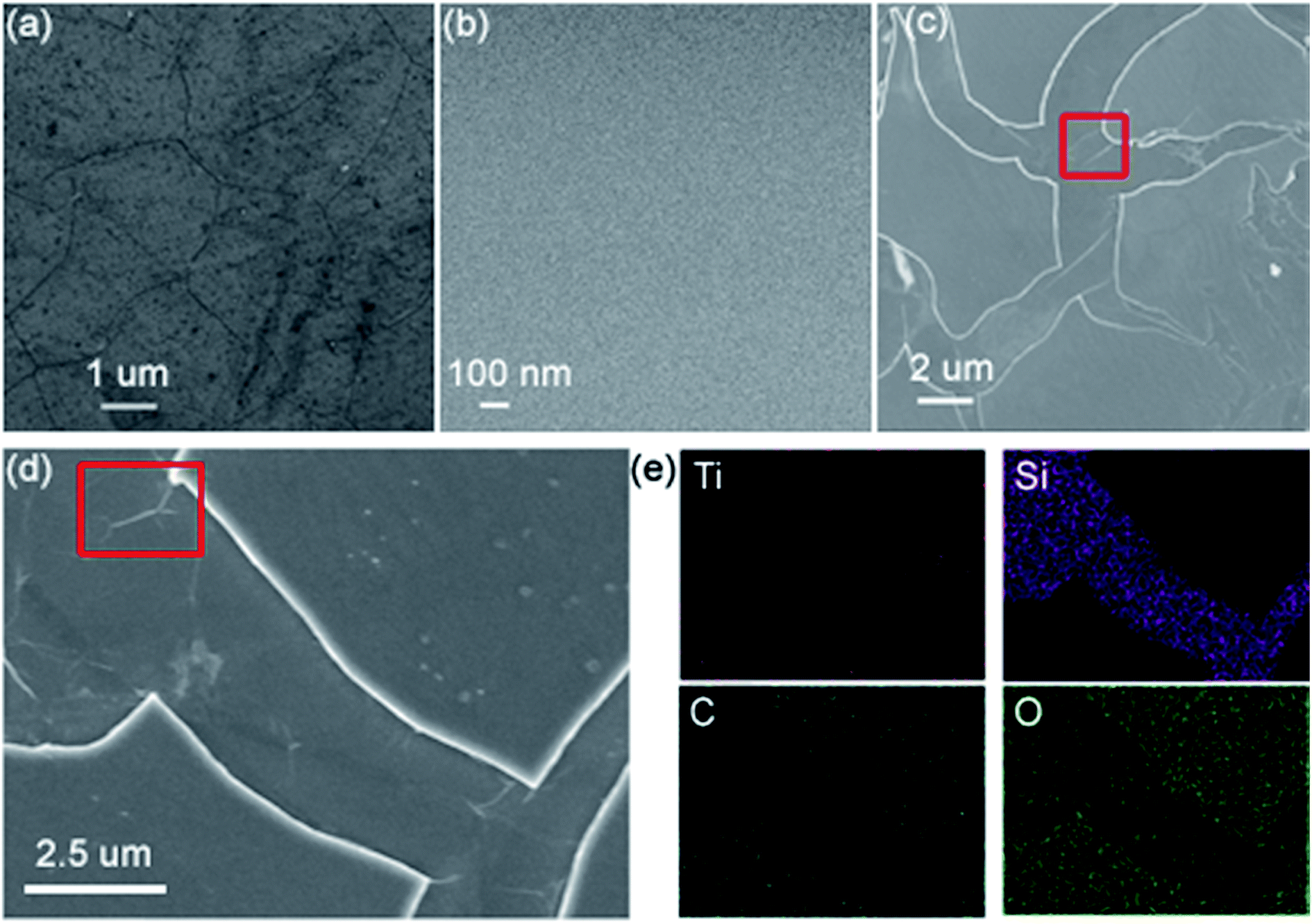 | ||
| Fig. 2 (a) The SEM image of graphene on SiO2/Si substrate transferred by PMMA, (b) the SEM image of pure TiO2 film produced by sol–gel method followed by annealing at 300 °C for 1 h. (c) The SEM image of graphene–TiO2 produced by sol–gel method followed by annealing at 300 °C for 1 h. (d) Enlarged SEM image of graphene–TiO2. (e) The corresponding EDS mapping for Ti, Si, C and O respectively for the same area in (d). The red rectangles in c and d indicate the wrinkles of graphene. | ||
Free of dangling bond, CVD graphene surface is hydrophobic with a surface free energy of 46.7 mJ m−2. Whereas, the TiO2 sol is hydrophilic with a surface free energy of 89 mJ m−2, as demonstrated in ref. 29. When the TiO2 sol was directly coated on the surface of graphene, dewetting occurred because of the disparity in the surface energies. Hence, cracks appear on the TiO2 layer after the thermal treatment, as shown in Fig. 2c. As wrinkle is a characteristic feature of transferred CVD graphene as shown in Fig. 2a, the existence of graphene can be identified in the graphene–TiO2 hybrid film from the cracks (Fig. 2c and d). Besides, a EDS mapping has been provided for the characterization of the microstructure (Fig. 2e). Based on the feature of Ti element mapping, the TiO2 layer can be identified. The C element mapping implies that there might be some residual carbon on the TiO2 layer after the annealing process. As the EDS mapping did on the SiO2/Si substrate, the Si and O elements can also be found.
To investigate whether graphene–TiO2 hybrid layer can be used as a substrate for Raman enhancement, the Raman spectra of molecules adsorbed on graphene–TiO2 hybrid layer were collected. In a typical process, Cu foil with graphene and TiO2 layer was transferred into etching solution. After thorough remove of the Cu foil, graphene coated with TiO2 layer was obtained, which is floating on the surface of the etching solution. Then, graphene coated with TiO2 layer was washed with water for three times and transferred to R6G aqueous solution with a series of concentrations from 1 × 10⁻⁶ M to 5 × 10⁻⁸ M for molecule adsorption. Finally, such hybrid layer was picked up by SiO2/Si substrate and was ready for the collection of the Raman spectra. In the Raman characterization process, it is found that signals of the adsorbed molecules can only be detected on the graphene, while no signal of the adsorbed molecule can be detect on the surface of TiO2 as well as the SiO2/Si substrate. Thus when the molecule adsorb on the bottom surface of the hybrid layer or even on the top surface of the hybrid layer, signals of the adsorbed molecule can only be detected on the cracks. A scheme of the preparation and characterization process for the graphene–TiO2 hybrid film can be found in Fig. 3.
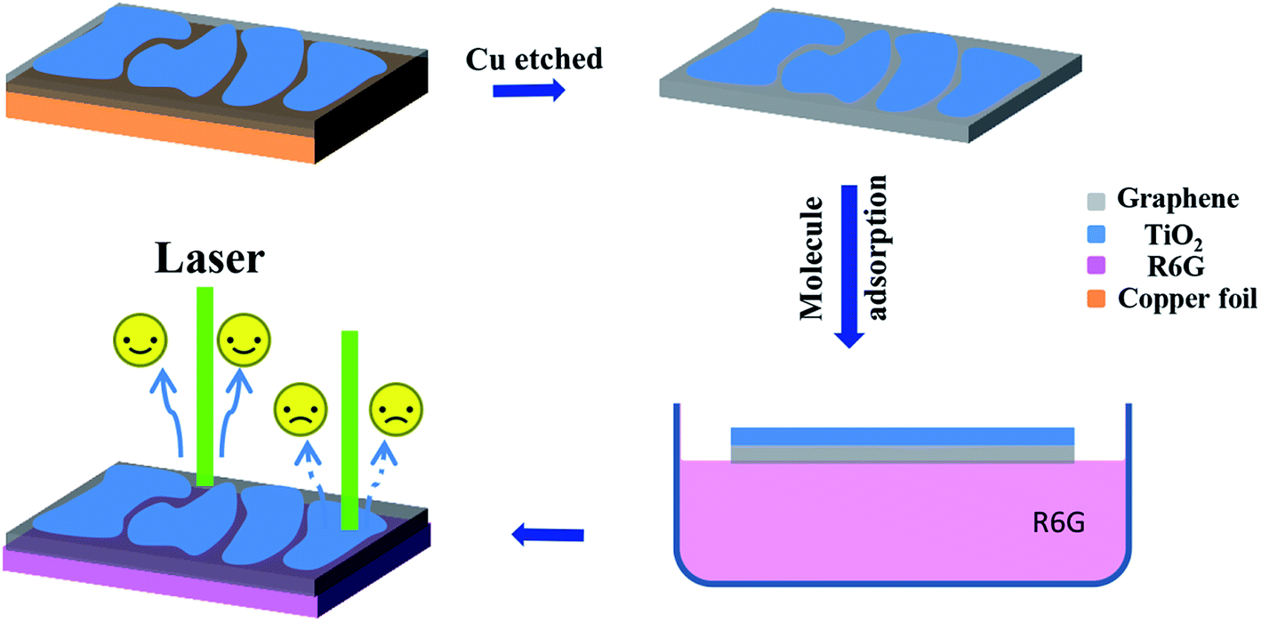 | ||
| Fig. 3 The scheme of the preparation and Raman characterization process for the graphene–TiO2 hybrid film. | ||
As shown in Fig. 4, the intensities of the Raman signals of the molecules on graphene decrease with the decrease in the concentration of solutions. Under concentration as low as 1 × 10⁻⁷ M, the Raman spectra keep whole characteristic peaks unambiguous. When the concentration decrease to 5 × 10⁻⁸ M, several characteristic peaks from the molecules can still be observed, such as 613, 1360 and 1647 cm−1. The concentration as low as 5 × 10⁻⁸ M is comparable with the concentration used in the classical SERS experiments. The appearance of the Raman signals for molecules on graphene under very low concentrations suggests that the graphene–TiO2 hybrid layer have Raman enhancement effect. Moreover, these results show that the graphene–TiO2 hybrid layer Raman enhancement effect should come from graphene.
 | ||
| Fig. 4 Raman spectra of R6G molecules adsorbed on the surface of graphene–TiO2 hybrid layer. The graphene were soaked by R6G aqueous solution and the concentration was 1 × 10⁻⁶ M (black line), 5 × 10⁻⁷ M (red line), 1 × 10⁻⁷ M (blue line) and 5 × 10⁻⁸ M (dark cyan line) respectively. | ||
TiO2 is wide band-gap semiconductor and it is reported that TiO2 could bring p-doping to graphene.27 Using TiO2 as a support layer, some change might be brought to the electronic structure of graphene and has some unknown influence on the Raman enhancement performance. In order to examine the effect of the TiO2 layer on the Raman enhancement of graphene, we characterized the SERS performance of the hybrid layer and compared it with that of graphene transferred with PMMA. The graphene–TiO2 hybrid layer and graphene transferred with PMMA are both used as surface enhanced Raman substrate respectively. In a typical process, the surface enhanced Raman substrate was transfer to 1 × 10⁻⁶ M R6G aqueous solution and float on the surface of the solution for 0.5 h. After being picked up by SiO2/Si substrate, the Raman signal of molecule adsorbed on graphene was collected. As shown in Fig. 5, Raman peaks at 613, 773, 1182, 1307, 1361, 1505, 1647 cm−1 are detected. Compared the two spectra in Fig. 5, it is found that features of the Raman spectroscopy are different. On the surface of graphene transferred by PMMA, peak at 1647 cm−1 is the strongest peak; however, on the surface of graphene–TiO2 hybrid layer, peak at 613 cm−1 is the strongest peak. After excluding the interference of fluorescence background, it seems that peaks at low wave numbers are even stronger than those at high wave numbers on the surface of graphene–TiO2 hybrid layer. In the literature, peak at 613 cm−1 could be assigned to Cx–Cx–Cx bend and peak at 773 cm−1 could be assigned to out-of-plane Cx–H bend, while peaks at 1182, 1307, 1361, 1505, 1647 cm−1 could be assigned to aromatic C–C stretching.30 Thus, graphene–TiO2 hybrid layer and graphene transferred by PMMA have different vibration-dependent Raman enhancement behavior. Here, we would give our speculation. With smooth surface and surface plasmon in the range of terahertz, the Raman enhancement effect of graphene can only originate from chemical mechanism.31 It is reported that the enhancement of different vibration modes could be ascribed to the dependence on the geometry of the molecules and the surface properties of Raman enhancement substrate.8,9,32 In accordance to previous reports, the R6G molecule adsorbs on the surface of graphene by π–π stacking. After the introduction of TiO2, the interaction between graphene and TiO2 would change the surface bonding properties of graphene and induce the surface polarization. Thus the interaction between graphene and R6G molecule would be changed, and probably even the geometry of the molecules on the surface. Such vibration dependence behavior of Raman enhancement is consistent with the chemical enhancement mechanism. To further study the interactions between TiO2 and graphene, XPS on the carbon K-edge is exploited to investigate the surface property as well as its evolution of graphene. The carbon K-edge XPS spectrum of graphene is given in Fig. S2.† In the XPS spectrum of graphene transferred by PMMA, a peak of sp2 carbon centered at 284.7 eV can be found, while the C 1s spectrum of graphene/TiO2 hybrid layer can be fitted by three components: a peak of sp2 carbon centered at 284.7 eV (P1), a weak peak at about 286.0 eV (P2) and another notable peak at 288.8 eV (P3). The observed large intensity of P1 implies that the structure of the basic graphene framework has been preserved in the graphene/TiO2 hybrid layer, while P2 and P3 peak might originate from sp3 hybridized carbon as well as other oxygen-containing groups. On the basis of previous studies, the oxygen-containing groups might induce larger surface dipoles.33 It is worth mentioning that graphene–TiO2 hybrid layer is probably better for application after further improvement of the Raman enhancement factor. As the D and G peaks of graphene overlap and interfere with the high-wave-number peaks, a much intense peak laying at low wave numbers would benefit the study of trace detection and the calculation of enhancement factor.
 | ||
| Fig. 5 Raman spectra of R6G molecules adsorbed on the surface of graphene. The black line represents that on graphene transferred by TiO2 layer and the red line represents that on graphene transferred by PMMA. All of Raman substrates based on graphene were soaked by 1 × 10⁻⁶ M R6G aqueous solution. | ||
Although TiO2 has no Raman enhancement for molecules, it could help develop a semiconductor–graphene system that combine the unique, yet complementary properties of either component to create a multipurpose device. In the rational designed hybrid structure, TiO2 is an effective photocatalyst, while graphene could enhance Raman signals for molecules and further promote the photocatalytic process for its outstanding charge-carrier transport property. After the remove of the Cu foil, a free standing graphene/TiO2 hybrid layer can be obtained, which can be transferred to various substrates (even the surface is uneven/curved), sense and degrade analyte in situ. In order to illustrate this point more clearly, we deposit a layer of R6G molecules on the SiO2/Si substrate and then transfer a free standing graphene/TiO2 hybrid film to it. Then it is found that the signals of the molecules on the surface of SiO2/Si substrate can be detected unambiguously (blue line in Fig. 6a). Then after 2 hours of irradiation by a 350 W xenon lamp, the molecules can be fully removed, because no signal of the molecule can be found (red line in Fig. 6a). For further investigation, graphene–TiO2 hybrid layer was soaked in 1 × 10⁻⁶ M R6G aqueous solution for molecule adsorption. After characterization with Raman microscope as shown in Fig. 6b (line 1a), the graphene–TiO2 hybrid layer was irradiated with xenon light for 1.5 h. The irradiation time was deliberately extended for the complete degradation. It could be found that there is not Raman peaks of R6G in line 1b after irradiation, which means that the molecules have been totally removed. In Fig. 6b, line 1a (the magenta line, 1a) is the Raman spectra for the first cycle. Then the irradiated graphene–TiO2 hybrid layer was soaked in R6G aqueous solution of the same concentration and the Raman signals for molecules was collected under the same experiment conditions once more. The dark cyan line (line 2) in Fig. 6b is the Raman spectrum after the re-adsorption process, which exhibit an excellent repeatability. The irradiation and re-adsorption process were repeated five times. In Fig. 6b, Raman spectra from the five cycles of the reusability test could be found. After 3 cycles, the intensities of the Raman peaks decrease to about sixty percent of the initial value and the vibration dependent Raman enhancement become to be similar with that of pure graphene. Such changes are supposed to be owing to the loss of TiO2 flakes for the weak surface interaction between graphene and TiO2, which should be further optimized in the following work.
 | ||
| Fig. 6 (a) Raman spectra of R6G molecules deposited on the surface of SiO2/Si substrate detected (blue line) and degraded (red line) with graphene–TiO2 hybrid layer in situ. (b) Raman spectra of R6G molecules adsorbed on the surface of graphene–TiO2 hybrid layer after five cycles reusability test. The number represent the time of cycle. Line numbered 1a (magenta line) represents the Raman spectra obtained for the first time and line numbered 1b (dark yellow line) represents the Raman spectra obtained after photo-catalysis. The peak at 520 cm−1 is from the SiO2/Si substrate. | ||
4. Conclusions
During the etching of the underlying copper, TiO2 was used as the supporting layer for graphene, and thus graphene–TiO2 hybrid film was prepared by a one-step transfer and integration method. Such hybrid film combines the function of detector and decomposer, which employs the CVD graphene as the SERS-active layer and TiO2 as the photocatalytic layer. In this study, its sensing and photocatalytic performances were characterized. It is found that its detection limit based on Raman enhancement is 5 × 10⁻⁸ M and could thoroughly decompose the contaminant effectively. This novel structure combines the complementary properties of graphene and TiO2, which is green, low-cost and simple in preparation. The application of it in integrated sensing and photocatalysis should be of value for fitting the wide range of requirements.Acknowledgements
This work was supported by the National Natural Science Foundation of China (11404001, 11374013, 51672001), the foundation of Co-operative Innovation Research Center for Weak Signal-Detecting Materials and Devices Integration Anhui University (Y01008411), the PhD Start-up Fund of Anhui University (No. 33190209).Notes and references
- K. Kneipp, Y. Wang, H. Kneipp, L. T. Perelman, I. Itzkan, R. Dasari and M. S. Feld, Phys. Rev. Lett., 1997, 78, 1667–1670 CrossRef CAS.
- S. M. Nie and S. R. Emery, Science, 1997, 275, 1102–1106 CrossRef CAS PubMed.
- X. M. Qian, X. H. Peng, D. O. Ansari, Q. Yin-Goen, G. Z. Chen, D. M. Shin, L. Yang, A. N. Young, M. D. Wang and S. M. Nie, Nat. Biotechnol., 2008, 26, 83–90 CrossRef CAS PubMed.
- K. A. Willets and R. P. Van Duyne, Localized surface plasmon resonance spectroscopy and sensing, Annu. Rev. Phys. Chem., 2007, 58, 267–297 CrossRef CAS PubMed.
- G. A. Baker and D. S. Moore, Anal. Bioanal. Chem., 2005, 382, 1751–1770 CrossRef CAS PubMed.
- M. K. Fan, G. F. S. Andrade and A. G. Brolo, Anal. Chim. Acta, 2011, 693, 7–25 CrossRef CAS PubMed.
- Z. Q. Tian, B. Ren and D. Y. Wu, J. Phys. Chem. B, 2002, 106, 9463–9483 CrossRef CAS.
- X. Ling, W. J. Fang, Y. H. Lee, P. T. Araujo, X. Zhang, J. F. Rodriguez-Nieva, Y. X. Lin, J. Zhang, J. Kong and M. S. Dresselhaus, Nano Lett., 2014, 14, 3033–3040 CrossRef CAS PubMed.
- J. J. Lin, L. B. Liang, X. Ling, S. Q. Zhang, N. N. Mao, N. Zhang, B. G. Sumpter, V. Meunier, L. M. Tong and J. Zhang, J. Am. Chem. Soc., 2015, 137, 15511–15517 CrossRef CAS PubMed.
- W. G. Xu, N. N. Mao and J. Zhang, Small, 2013, 9, 1206–1224 CrossRef CAS PubMed.
- H. Xu, Y. B. Chen, W. G. Xu, H. L. Zhang, J. Kong, M. S. Dresselhaus and J. Zhang, Small, 2011, 7, 2945–2952 CrossRef CAS PubMed.
- X. X. Yu, H. B. Cai, W. H. Zhang, X. J. Li, N. Pan, Y. Luo, X. P. Wang and J. G. Hou, ACS Nano, 2011, 5, 952–958 CrossRef CAS PubMed.
- J. Y. Liu, H. B. Cai, X. X. Yu, K. Zhang, X. J. Li, J. W. Li, N. Pan, Q. W. Shi, Y. Luo and X. P. Wang, J. Phys. Chem. C, 2012, 116, 15741–15746 CAS.
- W. G. Xu, J. Q. Xiao, Y. F. Chen, Y. B. Chen, X. Ling and J. Zhang, Adv. Mater., 2013, 25, 928–933 CrossRef CAS PubMed.
- G. R. S. Iyer, J. Wang, G. Wells, S. Guruvenket, S. Payne, M. Bradley and F. Borondics, ACS Nano, 2014, 8, 6353–6362 CrossRef CAS PubMed.
- K. C. Hsu and D. H. Chen, ACS Appl. Mater. Interfaces, 2015, 7, 27571–27579 CAS.
- I. K. Konstantinou and T. A. Albanis, Appl. Catal., B, 2004, 49, 1–14 CrossRef CAS.
- A. Fujishima, X. T. Zhang and D. A. Tryk, Surf. Sci. Rep., 2008, 63, 515–582 CrossRef CAS.
- X. B. Chen, S. H. Shen, L. J. Guo and S. S. Mao, Chem. Rev., 2010, 110, 6503–6570 CrossRef CAS PubMed.
- H. Tong, S. X. Ouyang, Y. P. Bi, N. Umezawa, M. Oshikiri and J. H. Ye, Adv. Mater., 2012, 24, 229–251 CrossRef CAS PubMed.
- G. Williams, B. Seger and P. V. Kamat, ACS Nano, 2008, 2, 1487–1491 CrossRef CAS PubMed.
- K. Woan, G. Pyrgiotakis and W. Sigmund, Adv. Mater., 2009, 21, 2233–2239 CrossRef CAS.
- H. Zhang, X. J. Lv, Y. M. Li, Y. Wang and J. H. Li, ACS Nano, 2010, 4, 380–386 CrossRef CAS PubMed.
- Q. J. Xiang, J. G. Yu and M. Jaroniec, Chem. Soc. Rev., 2012, 41, 782–796 RSC.
- D. V. Bavykin, J. M. Friedrich and F. C. Walsh, Adv. Mater., 2006, 18, 2807–2824 CrossRef CAS.
- X. Chen and S. S. Mao, Chem. Rev., 2007, 107, 2891–2959 CrossRef CAS PubMed.
- H. J. Jeong, H. Y. Kim, H. Jeong, J. T. Han, S. Y. Jeong, K. J. Baeg, M. S. Jeong and G. W. Lee, Small, 2014, 10, 2057–2066 CrossRef CAS PubMed.
- Y. Li, W. J. Wu, P. Dai, L. L. Zhang, Z. Q. Sun, G. Li, M. Z. Wu, X. S. Chen and C. L. Chen, RSC Adv., 2014, 4, 23831–23837 RSC.
- R. Wang, K. Hashimoto, A. Fujishima, M. Chikuni, E. Kojima, A. Kitamura, M. Shimohigoshi and T. Watanabe, Nature, 1997, 388, 431–432 CrossRef CAS.
- P. Hildebrandt and M. Stockburger, J. Phys. Chem., 1984, 88, 5935–5944 CrossRef CAS.
- X. Ling, L. M. Xie, Y. Fang, H. Xu, H. L. Zhang, J. Kong, M. S. Dresselhaus, J. Zhang and Z. F. Liu, Nano Lett., 2010, 10, 553–561 CrossRef CAS PubMed.
- X. Ling, J. X. Wu, W. G. Xu and J. Zhang, Small, 2012, 8, 1365–1372 CrossRef CAS PubMed.
- X. X. Yu, H. B. Cai, W. H. Zhang, X. J. Li, N. Pan, Y. Luo, X. P. Wang and J. G. Hou, ACS Nano, 2011, 5, 952–958 CrossRef CAS PubMed.
Footnotes |
| † Electronic supplementary information (ESI) available. See DOI: 10.1039/c7ra00252a |
| ‡ These two authors contribute equally to this work. |
| This journal is © The Royal Society of Chemistry 2017 |