
 Open Access Article
 This Open Access Article is licensed under a
 Creative Commons Attribution 3.0 Unported Licence
Preparation and electromagnetic wave absorbing properties of 3D graphene/pine needle-like iron nano-acicular whisker composites
Tingkai Zhao *a,
Wenbo Jin*a,
Xianglin Jia,
Junjie Gaoa,
Chuanyin Xionga,
Alei Danga,
Hao Lia,
Tiehu Lia,
Songmin Shangb and
Zhongfu Zhouc
*a,
Wenbo Jin*a,
Xianglin Jia,
Junjie Gaoa,
Chuanyin Xionga,
Alei Danga,
Hao Lia,
Tiehu Lia,
Songmin Shangb and
Zhongfu Zhouc
aState Key Laboratory of Solidification Processing, Shaanxi Engineering Laboratory for Graphene New Carbon Materials and Application, School of Materials Science and Engineering, Northwestern Polytechnical University, Xi'an 710072, P. R. China. E-mail: ztk-xjtu@163.com
bInstitute of Textiles and Clothing, The Hong Kong Polytechnic University, Kowloon, Hong Kong, P. R. China
cDepartment of Physics, Aberystwyth University, Aberystwyth SY23 3FL, UK
First published on 14th March 2017
Abstract
The improvement of high reflection loss and broad frequency bandwidth for electromagnetic wave absorption materials is a long-term effort. The superb micro-structures of the absorber have significant impact on increasing reflection loss and broadening frequency bandwidth. Herein, we prepared 3D graphene by chemical vapor deposition and then 3D graphene/pine needle-like iron nano-acicular whisker composites were in situ synthesized by an electrochemical deposition process under an electric field using 3D graphene as substrate. The nano-acicular whiskers show different sizes and the mean diameter of the individual iron nano-acicular whiskers was about 150 nm. The saturation magnetization (MS) of the 3D graphene/iron nano-acicular whisker composite was about 42.65 emu g−1 and the coercivity (Hc) was 143 Oe, and it shows good magnetic properties. In the frequency range of 2–18 GHz, the reflection loss value of the graphene/iron nano-acicular whisker composites with a thickness of 2 mm could reach −12.81 dB at 10.95 GHz and the effective absorption bandwidth below −10 dB was 2.16 GHz. The nano-acicular whiskers could effectively improve the electromagnetic wave absorbing properties. The results suggested that the as-prepared graphene/iron nano-acicular whisker nanocomposite showed great potential applications as a new absorber material.
Introduction
Electromagnetic (EM) wave absorbing materials have attracted great technical and scientific interest due to their extensive applications including in military and civilian areas.1 With the development of radar technology, stealth aircraft and warships show a strong viability and the invisibility of military equipment puts forward higher requirements on the microwave absorption materials.2 In addition, in recent years, a series of serious electromagnetic interference problems arose due to the multiplication of electronic products and devices in wireless communication tools, local area networks and other communication equipment.3 To solve these problems, considerable interest has been attracted to EM wave absorbing materials with higher efficiency and wider bandwidths. For a high performance EM wave absorbing material, excellent dielectric loss and magnetic loss are two important technical requirements.4 Carbon materials have been widely used as EM wave absorbing materials due to their lightweight, high conductivity, high stability and good dielectric properties, such as carbon nanotubes and graphene. However, the metal materials have good dielectric loss and show better magnetic loss than carbon materials, such as nickel, iron, cobalt.5 To acquire excellent EM wave absorbing properties, carbon materials are often combined with metal materials as absorber materials. Furthermore, it is worth noting that metal material has a whisker form and it has many interesting properties.6Since the discovery of metal whisker in 1946, it has been paid much attention because of the excellent physical and chemical properties.7 The whisker interior atoms are completely aligned in the same direction and position, forming an ideal crystal without any defects and having a high tensile strength.8,9 According to the previous reports,10–12 the strength of iron whisker is more than 100 times of the ordinary iron strength. In addition, they have good chemical stability, anti-high temperature, anti-oxidation and EM wave absorption performance. Zinc oxide whiskers have been used as absorber materials.13 However, the use of iron whiskers to do the absorber materials has not been reported. One of the important reasons is that the whisker is difficult to prepare. To obtain whisker, metal crystals can be placed for a long time to form metal whisker naturally. It can also be manufactured by artificial methods: one is evaporation coagulation method, the whisker material is sublimated or vaporized under vacuum or inert gas atmosphere environment and solidified at low temperature to form whisker; the other is chemical reaction method, as the reduction reaction of raw materials and furnace gas occurs, the whisker will grow. The synthesis method was selected according to different metal materials and iron whisker often use the chemical reaction method.14–16 However, above mentioned methods are too complex and costly, what's more, the size of these iron whiskers reported in the literatures is from 2 to 20 μm and the whisker size is so large that not conducive to the electromagnetic wave absorption. Graphene has excellent optical, electric and magnetic properties due to its unique single-layer carbon atomic structure and it has shown great potential application in many fields.17–19 EM wave absorption is one of an important application of graphene. For improving the EM wave absorption properties, graphene has been extensively compounded with other materials, such as metal material. Graphene/metal composite is usually prepared by two methods, that is, in situ synthesis and precipitation methods. The in situ synthesis method is that using metal substrate as the catalyst, graphene is formed on the metal surface by chemical vapor deposition (CVD) to obtain graphene/metal composite, and this method is also costly. Precipitation method is that metal ions and precipitants are added into graphene hydrogel successively to get metal hydroxide precipitated on the graphene surface, the product is freeze-dried and reduced to obtain graphene/metal composite, but this synthesis process is too complex.20–23 Xingchen Zhao24 et al. have reported the preparation of graphene-coated Fe nanocomposite and studied its EM wave absorption property, and this method they used is too complex and pollute environment.
In this paper, we used a new way to prepare iron whiskers. First, 3D GNs were prepared by CVD method using nickel foam as the substrate, and then the 3D graphenes/iron nano-acicular whisker composites (3D GNs/INAW) was successfully in situ prepared by electrochemical deposition method under the electric field using 3D GNs as substrate. It should be expected for using as the absorber material in the electromagnetic wave absorption. The microwave absorbing properties of the nanocomposites have been studied. Moreover, the EM wave absorption performance of graphene and iron whisker composites has not been reported before.
Experimental section
Preparation of 3D GNs
3D GNs were prepared by CVD method using nickel foam as substrate.25 The nickel foam which cut the size of 10 mm (length) × 10 mm (width) × 2 mm (height) was washed by ultrasonic washing with ethanol and deionized water successively and dried in vacuum oven. The treated nickel foam was placed into a tube furnace under a mixed H2/Ar/CH4 atmosphere at 1000 °C for 5 minutes to deposit 3D GNs on this foam structure. The obtained graphene/nickel foam was immersed into HCl solution (3 M) at 80 °C for 7 hours to etch away metal nickel, and then washed with deionized water to get pure 3D GNs.Synthesis of 3D GNs/INAW composites
The 3D GNs/INAW composites were synthesized and the schematic diagram is shown in Fig. 1. For the synthesis of 3D GNs/INAW composites, a certain amount of FeCl2 (1.5 M) and KCl (0.6 M) solutions were added into a plating tank, and a small amount of iron powders were placed into the plating tank to prevent the ferrous ion from being oxidated and hydrolyzed.26,27 The as-prepared 3D GNs were electrodeposited in plating tank placed in electric field at 25 °C under the electric current of 0.2 A and the electrodeposition time was 5 minutes. After the deposition, the 3D GNs/INAW composites containing few impurities were obtained. Then the products were acid-treated in HCl (1.5 M) solution for 3 minutes, washed with deionized water and dried in vacuum oven. Finally the resulting products were placed into a tube furnace with a hydrogen flow rate of 250 mL min−1 at 450 °C for 2.5 hours to remove the oxides produced during the drying process, then cooled down to room temperature and the 3D GNs/INAW composites were obtained. | ||
| Fig. 1 The schematic diagram of the synthesis process of 3D GNs/INAW composites. | ||
Characterizations and microwave absorption measurements
The morphology and microstructure of 3D GNs and 3D GNs/INAW composites were characterized by scanning electron microscope (SEM, Hitachi S-4800, Japan) containing energy dispersive spectrometer (EDS) and transmission electron microscope (TEM, JEM-100CX11, FEI). Raman spectra of samples were measured using a Lab RAM HR confocal Raman system with 532 nm diode laser excitation at room temperature. X-ray diffraction (XRD, X'Pert Pro, PANalytical; with Cu Kα radiation) patterns were recorded to identify the phase structure. The hysteretic loops of samples were measured using Vibrating Sample Magnetometer (VSM, Lake Shore 7410, Quantum Design). The reflection loss of composite films was measured by a network analyzer (Agilent technologies E8362B; 10 MHz to 20 GHz).For EM parameter measurements, 3D GNs/INAW composites were uniformly mixed with 90 wt% paraffin, and the compounds were poured into the planar rectangular mold and dried about 24 hours in the air. The prepared films were tailored precisely to the size of a rectangular waveguide (22.86 mm × 10.16 mm) for EM wave parameters test.
Results and discussion
Characterization of 3D GNs and 3D GNs/INAW composites
The SEM images of 3D GNs, 3D GNs/INAW and INAW are shown in Fig. 2. It exhibits the microstructure of 3D GNs, 3D GNs/INAW and INAW. Fig. 2a shows that the 3D GNs have a translucent 3D connected network structure and the skeleton is the same as nickel foam. The wall of 3D GNs is so thin that the 3D network structure has a certain degree of damage. Fig. 2b is the high magnification of 3D GNs, it shows that the surface of 3D GNs is composed of a number of graphene sheets which have a size of about 4 μm long and 3 μm wide. The surface of 3D GNs is incomplete due to the contamination of nickel foam and the lattice defects. In addition, there are some amorphous carbons as shown by the white particles in the figure and this is due to the formation of carbon sphere during the CVD pyrolysis of the gaseous carbon source. Fig. 2c shows the 3D GNs after the electrochemical deposition process, the surface of 3D GNs was covered with a plenty of INAW, iron particles and other impurities. The 3D structure is still maintained. Fig. 2d is the high magnification of the selected rectangular region of Fig. 2c. The surface of 3D GNs has been covered so much INAW that the graphene sheets almost could not be recognized. The INAW has rough surface with a lot of impurities and the whiskers are not randomly distributed. There exist a core and they show radial morphology with the core as a center, looking like pine needle shown as the picture on the right bottom corner in Fig. 2d. Fig. 2g is the EDS spectrum of the rectangular region selected in Fig. 2d. Apart from C and Fe, there also appear O and Ni peaks and it means that there exists some Ni and oxide impurities on the surface of INAW.28 Fig. 2e is the high magnification SEM image of INAW. It is obvious to see that there are some iron nanoparticles and oxide impurities attached on the surface of INAW. Fig. 2f is the whisker after acid treatment and the low magnification image on the left bottom corner, the micromorphology of iron whiskers was observed clearly. It illustrates that the most of the oxide impurities and iron particles have been removed from the surface of INAW, the surface become pure and smooth. The as-prepared pine needle-like iron nano-acicular whisker constructed together with 3D GNs and the structures of iron whisker are similar with the pine needle and have a core, the average diameter of iron nano-acicular whisker structure is about 5 μm. They show radial morphology with the core as a center, and the mean whisker diameter of the individual iron nano-acicular whisker is about 150 nm. | ||
| Fig. 2 (a) SEM image of 3D GNs. (b) High magnification SEM images of 3D GNs, (c) the 3D GNs after electrochemical deposition, (d) the high magnification SEM images of Fig. 1c and a pine needle on the right corner, (e) the high magnification SEM image of INAW, (f) the iron whisker after acid treatment and the macro image on the left corner, (g) the EDS spectrum image of the rectangular region selected in Fig. 1d. | ||
The TEM images of 3D GNs and INAW are shown in Fig. 3. It is obvious to see that the graphene with a lot of folds are very thin and showed a translucent film in Fig. 3a. It also can be seen that there are some iron particles on the surface of graphene. The high magnification of graphene on the upper right corner indicates that the edge of graphene is clear. The layer numbers of the graphene sheets are few. Fig. 3b is the image of INAW. The mean size of INAW is about 90 nm and it may be part of the tip of INAW. Moreover, it can be found that the surface of INAW is smooth.
 | ||
| Fig. 3 TEM images of (a) 3D GNs and (b) INAW. | ||
Fig. 4a is the Raman spectra of 3D GNs and 3D GNs/INAW composites. It can be seen that 3D GNs and 3D GNs/INAW composite mainly has three peaks, D peak (1350 cm−1), G peak (1580 cm−1) and 2D peak (2680 cm−1). D peak is the defect peak, and the smaller ID/IG is, the higher graphene crystallinity is. The number of layers of graphene was calculated using the ratio of I2D/IG, the layers increased with the ratio of I2D/IG.29 In the figure, the small ID/IG ratio indicates that the graphene defects are less, and I2D/IG ≈ 0.5 means that the number of graphene layers is about 4 layers. In addition, several peaks of Fe2O3 appear on the Raman spectrum of 3D GNs/INAW composites, and it displays that a number of iron whiskers were oxidized. Fig. 4b depicts the XRD patterns of 3D GNs and 3D GNs/INAW. It can be seen that the 3D GNs have an obvious peak at 26.8 degree and it represents the graphene phase. From the XRD pattern of 3D GNs/INAW, it can be found that there are six main peaks and the strong peaks are Fe (110), Ni (200) and C (002). Furthermore, the prepared composite also exist the peak of Fe2O3, Ni and C (the peak of 3D GNs), it indicates that there exist some Ni and oxide impurities.30 The presence of Ni and Fe2O3 is due to the fact that the nickel foam was not completely etched away and oxygen in the air oxidized a small amount of iron.
 | ||
| Fig. 4 (a) Raman spectra of 3D GNs and 3D GNs/INAW composites, (b) XRD patterns of 3D GNs and 3D GNs/INAW composites. | ||
Magnetic properties
An optical picture of 3D GNs/INAW composites is shown in Fig. 5 on the right bottom corner, it reveals that the magnetism of 3D GNs/INAW composite is very strong. Fig. 5 shows the hysteretic loops of pure 3D GNs and 3D GNs/INAW composites, curve (A) is the hysteretic loop of pure 3D GNs. It shows that pure 3D GNs are non-magnetic. Curve (B) is the hysteretic loop of 3D GNs/INAW composite, and it is similar with the hysteretic loop of pure Fe. Curve (C) is the partial amplification drawing of curve (B), and it shows that the curvature of saturation hysteretic loop of the magnetic nanoparticles is large and the magnetism of 3D GNs/INAW composite is strong. The saturation magnetization (MS) is about 42.65 emu g−1 and the coercivity (Hc) is 143 Oe. The results illustrate that the surface of 3D GNs modified by INAW is magnetization and ferromagnetism.31 Therefore, the 3D GNs/INAW composite has good magnetism and is easy to be adsorbed by magnet (this result is coincident with that of the optical picture in Fig. 5).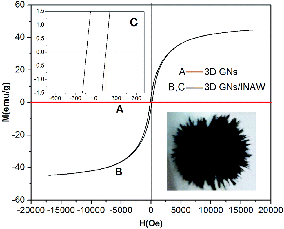 | ||
| Fig. 5 Optical picture and the hysteretic loops of 3D GNs/INAW composites. | ||
Electromagnetic wave absorbing properties
The complex permittivity (ε′, ε′′), permeability (μ′, μ′′), dielectric loss tangent (tan![[thin space (1/6-em)]](https://www.rsc.org/images/entities/char_2009.gif) δε) and magnetic loss tangent (tanδμ) spectra of 3D GNs and 3D GNs/INAW composite film vs. frequency are shown in Fig. 6. It illustrates the dielectric properties of 3D GNs and 3D GNs/INAW composite. Fig. 6a shows the complex permittivity of 3D GNs and 3D GNs/INAW composite in the frequency range of 8.2–12.4 GHz. The real part of these permittivity decrease with frequency increasing and the 3D GNs has a significant decline at 10.5 GHz. The imaginary part of 3D GNs/INAW is steady while the 3D GNs has a fluctuation at 10.5 GHz. The real and imaginary parts of 3D GNs and 3D GNs/INAW composites are very close and it is owing to the excellent dielectric properties of iron whiskers. The permeability (μ′, μ′′) is shown in Fig. 6b that μ′ and μ′′ values are complex and low compared with permittivity on account of their weak magnetic properties.
δε) and magnetic loss tangent (tanδμ) spectra of 3D GNs and 3D GNs/INAW composite film vs. frequency are shown in Fig. 6. It illustrates the dielectric properties of 3D GNs and 3D GNs/INAW composite. Fig. 6a shows the complex permittivity of 3D GNs and 3D GNs/INAW composite in the frequency range of 8.2–12.4 GHz. The real part of these permittivity decrease with frequency increasing and the 3D GNs has a significant decline at 10.5 GHz. The imaginary part of 3D GNs/INAW is steady while the 3D GNs has a fluctuation at 10.5 GHz. The real and imaginary parts of 3D GNs and 3D GNs/INAW composites are very close and it is owing to the excellent dielectric properties of iron whiskers. The permeability (μ′, μ′′) is shown in Fig. 6b that μ′ and μ′′ values are complex and low compared with permittivity on account of their weak magnetic properties.
 | ||
| Fig. 6 (a) Complex permittivity (ε′, ε′′), (b) permeability (μ′, μ′′) and (c) the dielectric loss tangent (tanδε) and magnetic loss tangent (tanδμ) spectra of 3D GNs and 3D GNs/INAW composites film vs. frequency, (d) reflection loss of 3D GNs and 3D GNs/INAW composite with different thicknesses vs. frequency in the range of 2–18 GHz. | ||
The value of μ′ and μ′′ of 3D GNs is in the vicinity of 1 and 0, respectively and it is mainly owing to the poor magnetic properties of 3D GNs. As for the 3D GNs/INAW composite, it shows a higher permeability (μ′, μ′′) values in the frequency of 8.2–12.4 GHz compared to 3D GNs. It is due to the magnetic properties of iron whisker. According to the experimental results for the EM parameters from Fig. 5a and b, the dielectric loss (tanδε) and magnetic loss (tanδμ) were calculated as shown in Fig. 6c in the frequency range of 8.2–12.4 GHz. It is known to us that the loss tangent means the loss properties of incidence EM wave in the microwave absorber. In general, the large loss tangent is expected. Fig. 6c shows that tanδε was comparatively higher than tanδμ regardless of the frequency and the type of absorbent. Thus, the reflection loss is mainly decided by the dielectric loss. From the comparison of tanδε and tanδμ of 3D GNs and 3D GNs/INAW composites in Fig. 6c, it finds that the tanδε of 3D GNs/INAW composites are steady relatively and greater in a large frequency range than 3D GNs. In addition, the tanδμ is also greater than 3D GNs almost in the whole frequency range. It is due to the poor magnetic loss of 3D GNs and 3D GNs/INAW composites has both dielectric loss and magnetic loss.32–34
For single-layer absorber, according to the transmission theory,35 the calculation formulas were given as follows eqn (1) and (2):
 | (1) |
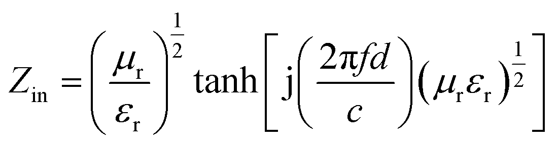 | (2) |
The reflection loss of 3D GNs and 3D GNs/INAW composite are shown in Fig. 6d. It indicates that 3D GNs/INAW composite exhibit better microwave absorption in the same thickness (2 mm) compared to 3D GNs. The minimum reflection loss values of pure 3D GNs and 3D GNs/INAW composite is −6.43 dB at 7.28 GHz and −12.81 dB at 10.95 GHz, respectively. The bandwidth of the reflectivity below −5 dB reach 5.51 GHz, the absorption bandwidth (<−10 dB) increase from 0 to 2.16 GHz and the reflection peak shift to higher frequency region. It is mainly due to that iron whisker improved the electromagnetic properties of 3D GNs and caused an absorbing effect.43 Whisker material is conducive to the formation of the ideal network. It is easy to form a three-dimensional conductive web structure with a certain size when it is mixed with the matrix.44 The EM waves pass through the 3D web structure of INAW to produce induced current, and it could absorb the EM wave energy as heat emission. In addition, whisker material has a large aspect ratio. In the EM field, the sharp tip is easy to form a local strong electric field, and the limited conductivity causes the INAW needle to be polarized in a short time.45 In this case, each needle is used as an electrical dipole and incident electromagnetic waves will produce resonance, thus consuming the energy. Moreover, the INAW has significant magnetic losses due to its excellent magnetic properties.46 The minimum reflection loss shift to low frequency region with the thickness of 3D GNs/INAW composite increasing from 2 to 5 mm. In addition, the multiple absorbing peaks appear with the increasing of 3D GNs/INAW composite thickness, and the first absorbing peck bandwidths (<−10 dB) decrease. This may be due to the different travel path and time of incident microwave in the absorber with different thickness and the synergistic effect of microwave absorption. Table 1 shows the different magnetic particles/graphene composites and their properties. It indicates that 3D GNs/INAW composite has good EM wave absorbing performance compared to the published references. The reflection loss of 3D GNs/INAW composite was up to −12.81 dB and the frequency bandwidth could reach to 2.16 GHz in the frequency range of 2–18 GHz. The 3D GNs/INAW composite exhibits excellent EM wave absorbing properties, and it has potential application in the field of electromagnetic wave absorption.
Conclusions
3D GNs/INAW composites had been successfully synthesized through a simple electrochemical deposition process. The pine needle-like iron whiskers were uniformly deposited the surface of 3D GNs, and the structures of iron whiskers were similar with the pine needle and had a core, the average diameter of iron nano-acicular whisker structure was about 5 μm. They showed radial morphology with the core as a center, and the mean whisker diameter of the individual iron nano-acicular whisker was about 150 nm. The saturation magnetization (MS) of iron nano-acicular whisker composites was about 42.65 emu g−1 and the coercivity (Hc) was 143 Oe. The experimental results indicate that 3D GNs/INAW composites demonstrated much better characteristics of microwave absorption. In the frequency range of 2–18 GHz, the lowest reflection loss value of the 3D GNs/INAW composites with a thickness of 2 mm could reach −12.81 dB at 10.95 GHz and the effective absorption bandwidth below −10 dB was 2.16 GHz. The EM wave absorbing performance is mainly owing to the good magnetic properties of iron whisker and the synergistic effect of microwave absorption and electromagnetic matching. It shows that the iron nano-acicular whisker material can improve EM wave absorbing performance effectively and has potential applications.Acknowledgements
This work was supported by funding from the Natural Science Foundation of China (51572221, 51672221), China Aeronautical Science Fund (2014ZF53074), and the Graduate Starting Seed Fund of Northwestern Polytechnical University (Z2016002).References
- Y. Wu, M. Han, T. Liu and L. Deng, J. Appl. Phys., 2015, 118, 1301–1303 Search PubMed.
- H. Lv, G. Ji, H. Zhang and Y. Du, RSC Adv., 2015, 5, 76836–76843 RSC.
- X. Zhang, Y. Li, R. Liu, Y. Rao, H. Rong and G. Qin, ACS Appl. Mater. Interfaces, 2016, 8, 3494–3498 CAS.
- Y. Ding, L. Zhang, Q. Liao, G. Zhang, S. Liu and Y. Zhang, Nano Res., 2016, 9, 1–8 CrossRef.
- C. Tsonos, N. Soin, G. Tomara, B. Yang, G. C. Psarras, A. Kanapitsas and E. Siores, RSC Adv., 2015, 6, 1919–1924 RSC.
- L. Sun, L. Zhan, Y. Shi, L. Chu, G. Ge and Z. He, Synth. Met., 2014, 187, 102–107 CrossRef CAS.
- H. L. Cobb, Monthly Rev. Am. Electroplaters Soc., 1946, 33, 28–30 CAS.
- J. Stein, U. Welzel, A. Leineweber, W. Huegel and E. J. Mittemeijer, Acta Mater., 2015, 86, 102–109 CrossRef CAS.
- M. W. Barsoum, E. N. Hoffman, R. D. Doherty, S. Gupta and A. Zavaliangos, Phys. Rev. Lett., 2004, 93, 206104–206106 CrossRef CAS PubMed.
- T. Yanase, A. Kawahito, Y. Hashimoto, T. Endo, Y. Wang, T. Nagahama and T. Shimada, RSC Adv., 2014, 4, 27620–27624 RSC.
- G. Liu, L. Wang, G. Chen, S. Hua, C. Ge, H. Zhang and R. Wu, J. Alloys Compd., 2012, 514, 183–188 CrossRef CAS.
- A. Guillet, Mater. Lett., 2010, 64, 2148–2150 CrossRef CAS.
- L. Kong, X. Yin, F. Ye, Q. Li, L. Zhang and L. Cheng, J. Phys. Chem. C, 2016, 117, 2135–2146 Search PubMed.
- X. Gong, B. Zhang, Z. Wang and Z. Guo, Metall. Mater. Trans. B, 2014, 45, 2050–2056 CrossRef CAS.
- S. Palchoudhury, W. An, Y. Xu, Y. Qin, Z. Zhang, N. Chopra, R. A. Holler, C. H. Turner and Y. Bao, Nano Lett., 2011, 11, 1141–1146 CrossRef CAS PubMed.
- T. Macher, J. Totenhagen, J. Sherwood, Y. Qin, D. Gurler, M. S. Bolding and Y. Bao, Adv. Funct. Mater., 2015, 25, 490–494 CrossRef CAS.
- T. Zhang, Q. Xue, S. Zhang and M. Dong, Nano Today, 2012, 7, 180–200 CrossRef CAS.
- S. K. Hong, K. Y. Kim, T. Y. Kim, J. H. Kim, S. W. Park, J. H. Kim and B. J. Cho, Nanotechnology, 2012, 23, 1–8 CrossRef.
- Y. Zhu, S. Murali, W. Cai, X. Li, J. W. Suk, J. R. Potts and R. S. Ruoff, Adv. Mater., 2010, 22, 3906–3924 CrossRef CAS PubMed.
- Z. S. Wu, G. Zhou, L. C. Yin, W. Ren, F. Li and H. M. Cheng, Nano Energy, 2012, 1, 107–131 CrossRef CAS.
- M. S. Lee, K. Lee, S. Y. Kim, H. Lee, J. Park, K. H. Choi, H. K. Kim, D. G. Kim, D. Y. Lee and S. Nam, Nano Lett., 2013, 13, 2814–2821 CrossRef CAS PubMed.
- S. P. Pawar, M. Gandi and S. Bose, RSC Adv., 2016, 6, 37633–37645 RSC.
- C. Nethravathi, M. Rajamathi, N. Ravishankar, L. Basit and C. Felser, Carbon, 2010, 48, 4343–4350 CrossRef CAS.
- X. Zhao, Z. Zhang, L. Wang, K. Xi, Q. Cao, D. Wang, Y. Yang and Y. Du, Sci. Rep., 2013, 3, 182 Search PubMed.
- J. W. Suk, A. Kitt, C. W. Magnuson, Y. Hao, S. Ahmed, J. An, A. K. Swan, B. B. Goldberg and R. S. Ruoff, ACS Nano, 2011, 5, 6916–6924 CrossRef CAS PubMed.
- Y. H. Chang, C. T. Lin, T. Y. Chen, C. L. Hsu, Y. H. Lee, W. Zhang, K. H. Wei and L. J. Li, Adv. Mater., 2013, 25, 756–760 CrossRef CAS PubMed.
- C. Xiong, T. Li, A. Dang, T. Zhao, H. Li and H. Lv, RSC Adv., 2016, 5, 602–610 Search PubMed.
- X. Xu, H. Li, Q. Zhang, H. Hu, Z. Zhao, J. Li, J. Li, Y. Qiao and Y. Gogotsi, ACS Nano, 2015, 9, 3969–3977 CrossRef CAS PubMed.
- A. C. Ferrari, J. C. Meyer, V. Scardaci, C. Casiraghi, M. Lazzeri, F. Mauri, S. Piscanec, D. Jiang, K. S. Novoselov and S. Roth, Phys. Rev. Lett., 2006, 97, 13831–13840 Search PubMed.
- J. Benson, Q. Xu, P. Wang, Y. Shen, L. Sun, T. Wang, M. Li and P. Papakonstantinou, ACS Appl. Mater. Interfaces, 2014, 6, 19726–19736 CAS.
- C. L. Zhu, M. L. Zhang, Y. J. Qiao, G. Xiao, F. Zhang and Y. J. Chen, J. Phys. Chem. C, 2010, 114, 16229–16235 CAS.
- L. Kong, X. Yin, X. Yuan, Y. Zhang, X. Liu, L. Cheng and L. Zhang, Carbon, 2014, 73, 185–193 CrossRef CAS.
- J. Fang, T. Liu, Z. Chen, Y. Wang, W. Wei, X. Yue and Z. Jiang, Nanoscale, 2016, 8, 8899–8909 RSC.
- T. Wang, Y. Li, L. Wang, C. Liu, S. Geng, X. Jia, F. Yang, L. Zhang, L. Liu and B. You, RSC Adv., 2015, 5, 60114–60120 RSC.
- P. Liu, Y. Huang and X. Zhang, Mater. Lett., 2014, 136, 298–301 CrossRef CAS.
- H. Wang, Z. Yan, J. An, J. He, Y. Hou, H. Yu, N. Ma, G. Yu and D. Sun, RSC Adv., 2016, 6, 95–96 Search PubMed.
- B. Qu, C. Zhu, C. Li, X. Zhang and Y. Chen, ACS Appl. Mater. Interfaces, 2016, 8, 3730–3735 CAS.
- W. Y. Jin, B. L. Sang, G. S. Dong, K. L. Sang, K. H. Kim and O. Park, J. Alloys Compd., 2016, 663, 196–203 CrossRef.
- Z. Zhu, X. Sun, G. Li, H. Xue, H. Guo, X. Fan, X. Pan and J. He, J. Magn. Magn. Mater., 2015, 377, 95–103 CrossRef CAS.
- Y. Chen, Z. Lei, H. Wu, C. Zhu, P. Gao, Q. Ouyang, L. H. Qi and W. Qin, Mater. Res. Bull., 2013, 48, 3362–3366 CrossRef CAS.
- H. Zhang, A. Xie, C. Wang, H. Wang, Y. Shen and X. Tian, J. Mater. Chem. A., 2013, 1, 8547–8552 CAS.
- X. Ding, Y. Huang, S. Li and J. Wang, RSC Adv., 2016, 6, 31440–31447 RSC.
- L. Yuan, L. Xiang, L. Rong and L. Ying, RSC Adv., 2015, 5, 18660–18665 RSC.
- D. Sun, Q. Zou, Y. Wang, Y. Wang, W. Jiang and F. Li, Nanoscale, 2014, 6, 6557–6562 RSC.
- M. Han, X. Yin, S. Ren, W. Duan, L. Zhang and L. Cheng, RSC Adv., 2016, 6, 6467–6474 RSC.
- M. Han, X. Yin, L. Kong, M. Li, W. Duan, L. Zhang and L. Cheng, J. Mater. Chem. A, 2014, 2, 16403–16409 CAS.
| This journal is © The Royal Society of Chemistry 2017 |