
 Open Access Article
 This Open Access Article is licensed under a Creative Commons Attribution-Non Commercial 3.0 Unported Licence
Proximity correction and resolution enhancement of plasmonic lens lithography far beyond the near field diffraction limit†
Yunfei Luo‡
a,
Ling Liu‡ab,
Wei Zhanga,
Weijie Konga,
Chengwei Zhaoa,
Ping Gaoa,
Zeyu Zhaoa,
Mingbo Pua,
Changtao Wanga and
Xiangang Luo *a
*a
aState Key Laboratory of Optical Technologies on Nano-Fabrication and Micro-Engineering, Institute of Optics and Electronics, Chinese Academy of Sciences, P.O. Box 350, Chengdu 610209, China. E-mail: lxg@ioe.ac.cn
bUniversity of Chinese Academy of Sciences, Beijing 100049, China
First published on 21st February 2017
Abstract
Near-field optical imaging methods have been suffering from the issue of a near field diffraction limit, i.e. imaging resolution and fidelity depend strongly on the distance away from objects, which occurs due to the great decay effect of evanescent waves. Recently, plasmonic cavity lens with off-axis light illumination was proposed as a method for going beyond the near field diffraction limit for imaging dense nanoline patterns. In this paper, this investigation was further extended to more general cases for isolated and discrete line patterns, by enhancing the resolution and correcting the proximity effect with assistant peripheral groove structures. Experiment results demonstrate that the width of single, double and multiple line patterns is well controlled and the uniformity is significantly improved in lithography with a 365 nm light wavelength and 120 nm working distance, being approximately ten times the air distance defined by the near field diffraction limit. The methods are believed to find applications in nanolithography, high density optical storage, scanning probe microscopy and so forth.
1. Introduction
In conventional far-field optics, the imaging resolution is diffraction limited, as usually defined in the form of the Rayleigh–Abbe limit.1,2 In near field optics, the detection and employment of evanescent waves help to realize sub-diffraction imaging, as shown by scanning near field optical microscopes (SNOMs),3,4 and near field optical lithography.5–9Surface plasmon polaritons (SPPs) are coupled waves of electromagnetic fields and free electrons at the interface between dielectric and conducting media.10,11 SPPs exhibit unique sub-diffraction propagation features with much shorter propagation wavelengths than those in dielectric media, which was successfully applied for optical lithography beyond the diffraction limit.12–14 In 2000, Pendry pioneered the study of a superlens composed of a flat slab with negative permittivity, where excited surface plasmon polaritons help to amplify an object's evanescent waves, which would produce the super resolution images.15 Plasmonic imaging lithography based on superlens was demonstrated with a silver film positioned between mask and resist, with a half-pitch resolution below 60 nm.16–18 More recently, various plasmonic lens lithography were proposed for the improvement of resolution, aspect profile and imaging contrast, by using smooth superlens,19–21 metal reflector cladding,22–24 plasmonic cavity lens etc.,25,26 providing an efficient way for the fabrication of various nanostructures.27–29 Plasmonic cavity lens even has achieved resolution up to a half-pitch of 22 nm in experiment.30
The attainable resolution in conventional near field lithography and plasmonic lens lithography is mainly determined by the evanescent waves employed in imaging process, which decay abruptly with air distance away from mask patterns. So even small air separation between patterns and plasmonic lens would reduce resolution significantly, which could be evaluated by analyzing evanescent waves' exponentially decaying feature in air. This point could be referred to as the near-field diffraction limit.31,32 Resultantly, contacting mode or physically stacked mask pattern, superlens and even resist layer, is usually applied in experimental demonstrations of plasmonic lens lithography.6,18,22,33–40 This is clearly unexpected in practical applications, considering that some abrasions and contamination of mask patterns may occur in the lithography process and fine alignment would not be readily performed as masks are contacted with photoresist layers.
In our recent investigation, plasmonic cavity lens imaging with off-axis light illumination (OAI) was proposed an assistance to go beyond the near field diffraction limit, by separating mask patterns and lens with a large air spacer helping to facilitate lithography operation and protection of nano mask patterns.41 In this special case the air thickness is much larger than that defined by near field diffraction limit. However this investigation is only useful for patterns with periodical dense nano lines and hence suffers from greatly limited types of patterns. As for discrete and isolated nano lines, which are commonly used in logic integrated circuits,42,43 quantum chips44,45 and optical metamaterials46,47 etc., great proximity effect of image width and difference between edge and central lines hampers the resolution and fidelity of images.48
In this paper, we investigates further the plasmonic cavity lens lithography far beyond near field diffraction limit, in more general cases with single and multiple adjacent nano lines. Resolution enhancement and proximity correction are performed by utilizing peripheral assistant grooves and off-axis light illumination. Both numerical simulations and experimental results show that nano discrete lines could be well imaged with plasmonic lens lithography beyond near field diffraction limit. As shown in one example, nano-lines patterns with a feature size of 60 nm are imaged under 365 nm illumination light with 120 nm air space between the mask and plasmonic cavity lens, approximately 10 times longer than that in conventional near-field photolithography. It is believed that our method is potentially promising for applications such as nano fabrications, optical storage etc.
2. Experimental section
2.1 Numerical simulations
The electric field intensity distributions shown in Fig. 1–3 were simulated using a commercial Comsol software. Rigorous coupled wave analysis (RCWA) was applied to calculate the optical transfer function (OTF) as shown in Fig. 4 and the transmission amplitude distributions was shown in Fig. 5. The RCWA code was written based on the eqn given in ref. 49. The electric field intensity distributions shown in Fig. 6 and 7 were simulated using a commercial CST software. | ||
| Fig. 1 Simulated electric filed intensity of single silt for 60 nm feature size under NI with 80 nm air working distance. (a) Conventional near-field imaging under NI. (b) Superlens imaging under NI. (c) Plasmonic cavity lens imaging under NI, in the form of 20 nm thick Ag film, 30 nm thick Pr film and 50 nm thick Ag cladding. (d) Normalized electric field profiles of (a–c) at the central position of Pr layer. | ||
 | ||
| Fig. 2 Simulated electric filed intensity of single silt for 60 nm feature size at the centre of photoresist (Pr) layer of noncontact plasmonic lithography without or with grooves-assisted under NI with 120 nm air working distance. (a) Without assistance grooves at the mask pattern. (b) With assistance grooves at the mask pattern. (c) Normalized electric field profiles of (a, b) at the central of Pr layer. | ||
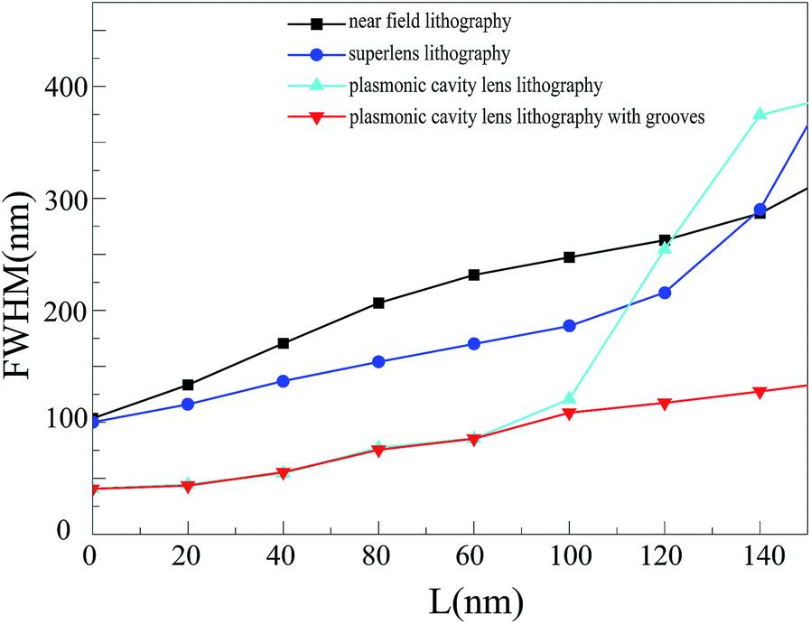 | ||
| Fig. 3 FWHM of a single line without or with grooves at the exit side of mask of near field optics, superlens lithography and plasmonic cavity lens imaging structures as a function of working distance under normal incidence (NI, kx,inc = 0). | ||
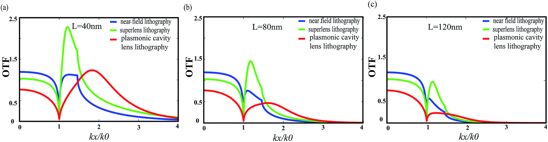 | ||
| Fig. 4 Calculated optical transfer functions (OTF) of different imaging configurations with work distance of 40 nm (a), 80 nm (b), 120 nm (c) respectively. The calculation plane is the central of Pr layer. | ||
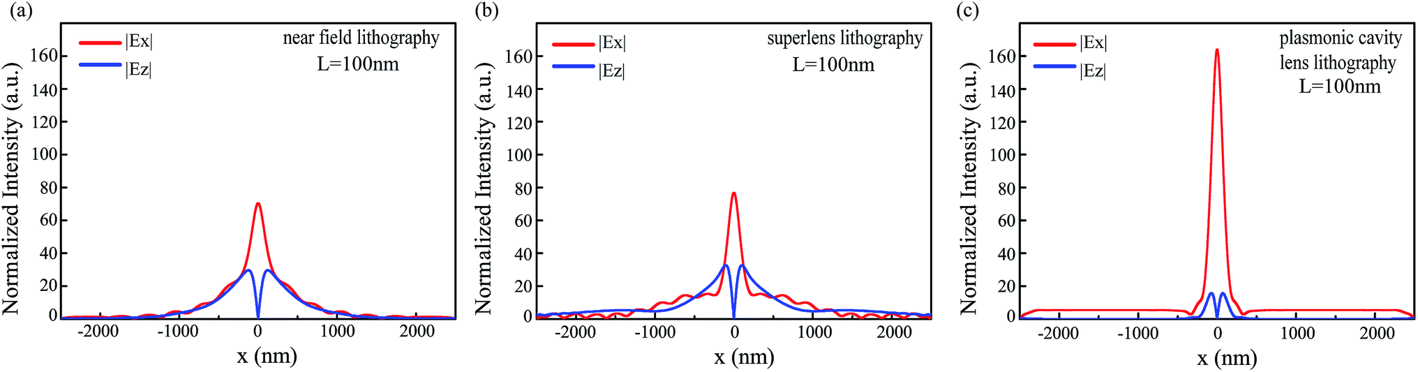 | ||
| Fig. 5 Transmission amplitude of the image plane in the measure of |Ex| and |Ez| for the near field lithography (a), superlens (b) and plasmonic cavity lens (c). The calculation plane is fixed at the centre of photoresist (Pr) layer. | ||
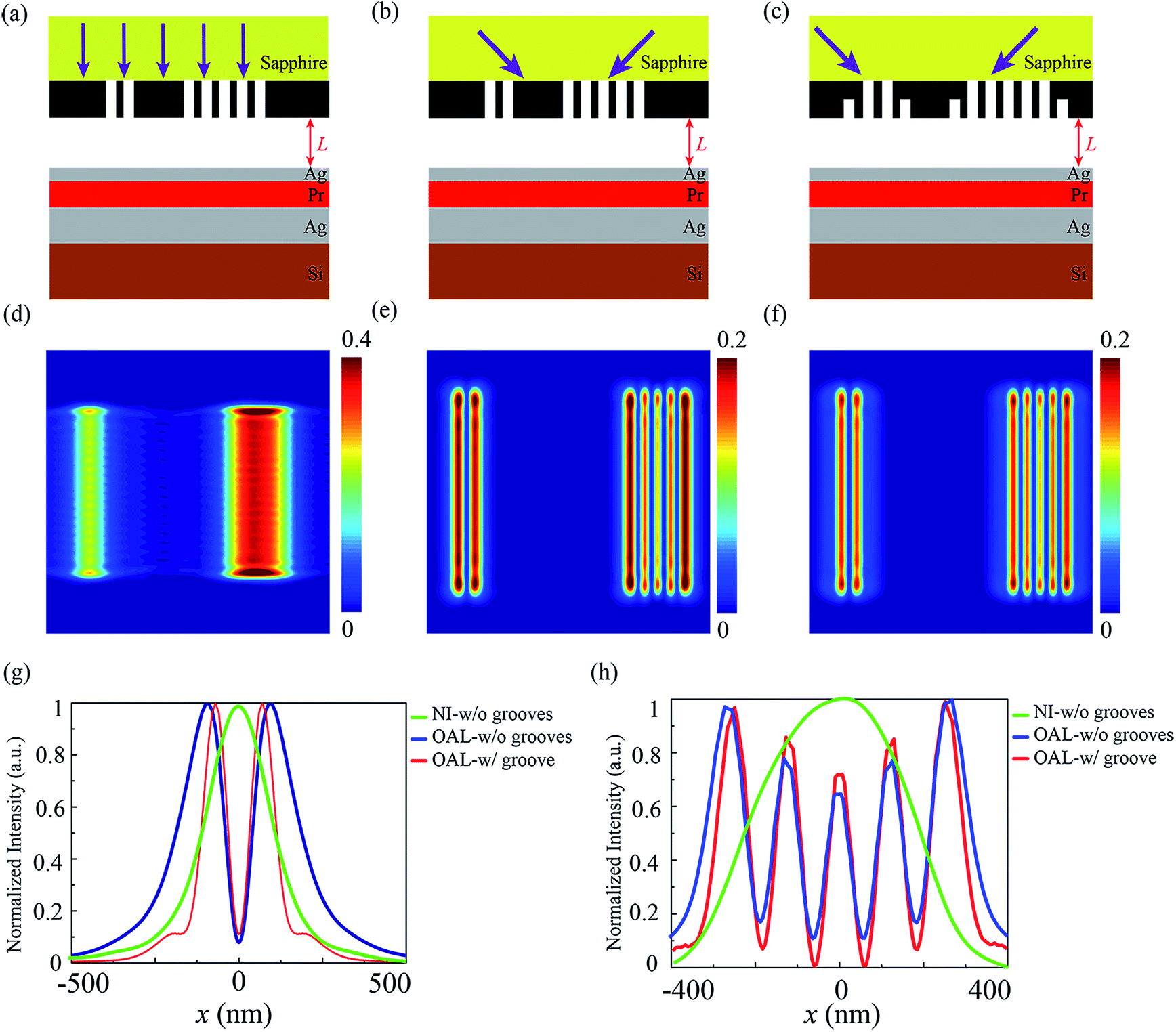 | ||
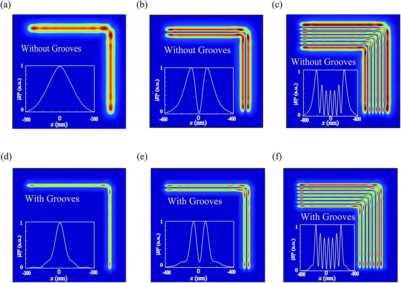
| Fig. 6 Schematic configuration and simulated electric filed intensity at the centre of photoresist (Pr) layer of noncontact plasmonic lithography without or with groove-assist under NI and OAI with 120 nm air working distance. The schematic configuration of plasmonic lithography without groove-assist under NI (a), and OAI (b), with groove-assist under OAI (c). The corresponding electric filed intensity (d–f) and normalized electric field profiles of double lines (g) and multiple lines (h) with 60 nm half-pitch at the central of Pr layer. | ||
 | ||
| Fig. 7 Calculated electric filed intensity of two-dimensional isolated patterns and multiple nano-lines patterns at the centre of photoresist (Pr) layer of noncontact plasmonic lithography without (a–c) or with (d–f) groove-assist under OAI (the insert is normalized electric field profiles of X direction at the central of Pr layer). | ||
2.2 Fabrication procedures for the plasmonic cavity lens and mask
For the Ag–PR–Ag plasmonic cavity structure, the 50 nm thick Ag film was firstly deposited on a fused silica substrate by the thermal evaporation at a base pressure of ∼5.0 × 10⁻⁴ Pa with deposition rate of 5 nm s−1. The AFM measured surface roughness (root-mean-square) was about 0.57 nm. About 30 nm thick photoresist of the diluted AR-P3170 (diluted by ALLRESIST GMBH, Strausberg, 30 nm@4000 rpm) was spun on the Ag layer to record the near-field images. After 5 min of the prebake of photo resist at 100 °C on hotplate, the surface roughness of photo resist was measured to be about 0.3 nm. Then, a 20 nm thick Ag film is evaporated on the photo resist (base pressure ∼ 5.0 × 10⁻⁴ Pa, deposition rate 1 nm s−1) and the measured roughness of the top surface is ∼0.43 nm (Fig. S2 in the ESI†).The fabrication of the Cr mask started from the deposition of Cr film by Magnetron Sputtering (RF power 400 W, deposition rate 0.5 nm s−1 and temperature 300 °C) onto a sapphire substrate. The thickness of the deposited Cr film was equal to the air distance. Then, photoresist of AZ 3100 (AZ Electronic Materials, 1 μm/4000 rpm) was spin-coated on the top of Cr film and a 10 μm wide window in the photoresist was realized by UV photolithography. The post-exposure window was developed by AZ 300MIF (AZ Electronic Materials) and was transferred into Cr film by wet etching. After that, the residual resist was removed by oxygen plasma etching with a power of 5 W and with O2 flow of 10 sccm for 2 minutes. Subsequently, the deposition of 40 nm Cr film was applied to achieve the Cr mask (Fig. S3(a) and (b) in the ESI†). Finally, nano-pattern object was milled on the mask by Focused Ion Beam (Helios Nanolab 650, FEI Company, @30 kV Accelerating Voltage).
2.3 Exposure and development procedures
The substrate with Ag–Pr–Ag plasmonic cavity lens was physically contacted with the Cr mask with a spacer around pattern regions to generate a fixed air gap and to avoid abrasion in the lithography process. The high-NA illumination light (NA = 1.5) was excited by plane wave vertically impinging on the upside-down isosceles trapeze sapphire prism under a 365 nm mercury lamp illuminating system. The exposure with an uniform flux of 1.0 mW cm−2 and exposure time ranging from 20 s to 50 s was applied in the experiment. Before the developing process, a physical method was used to peel off the top Ag layer. After that, the substrate with photoresist was developed by diluted AR 300-35 (ALLRESIST GMBH, Strausberg) with de-ionized water with the ratio of 1![[thin space (1/6-em)]](https://www.rsc.org/images/entities/char_2009.gif) :1 for 40 s at temperature 0 °C.
:1 for 40 s at temperature 0 °C.
2.4 Characterization
Scanning electron microscopy (SEM S-8010 HITACHI cool field emission) was used to characterize the topography of the lithography patterns. The samples were sputtered with several nanometers-thick Pt layer prior to imaging in order to reduce the charging effects. Atomic force microscope (NT-MDT) was used to characterize the surface roughness of the samples. The cross-sectional SEM image of the masks was fabricated by Focused Ion Beam with an incidence angle of 52°.3. Results and discussion
3.1 Simulations of plasmonic lens imaging with air separation in variant structures
To show the issue of near field diffraction limit and the difference between variant plasmonic lens designs, Fig. 1 shows the simulation imaging results of a single line pattern with the conventional near-field imaging, superlens and plasmonic cavity lens under normal incidence (NI, kx,inc = 0) light with 365 nm wavelength and transversal magnetic polarization. The mask is patterned with a 60 nm wide slit on a 90 nm thick Cr film. An air separation exists between mask pattern and lens or resist layer. The corresponding permittivities of the materials at 365 nm wavelength are εsapphire = 3.218, εCr = −8.9 + 9.0i, εAg = −2.4 + 0.24i, and εPr = 2.59, respectively.In the near-field lithography case shown in Fig. 1(a), where the mask is just positioned above the resist layer with an air space of 80 nm, the light transmitted through nano slit diffracts greatly and forms widened light field distribution in resist. Once the 20 nm thick Ag film, acting as a superlens, is positioned on the resist layer, the profile width of light distribution in the resist is clearly narrowed as shown in Fig. 1(b), due to the sub-wavelength imaging effect of the silver film. Further in Fig. 1(c), another bottom Ag film of 50 nm thickness is added below the resist layer, which in combination with the top Ag film forms a plasmonic cavity lens structure. Here, the image of the sandwiched resist exhibits much smaller width, indicating a considerable improvement of resolution as well as fidelity. The bottom Ag film thickness is larger than its skin depth here to avoid image degradation due to the SP mode coupling to the outer side of bottom Ag film. Fig. 1(d) plots the light distribution profiles at the middle plane of resist layer for the above three cases, showing full width at half maximum (FWHM) of 230 nm, 170 nm and 85 nm, respectively.
3.2 Proximity correction imaging with peripheral grooves
When the air distance is elongated to 120 nm, even the plasmonic cavity lens does not maintain its sub-wavelength imaging ability. As shown in Fig. 2(a), the image width of a slit for this case is broadened to about 250 nm, mainly due to the great decay of evanescent waves. The image here is even larger than superlens, indicating that evanescent waves could not be coupled into SP cavity mode and drop abruptly in magnitude for large air distance. This point could be viewed as a near field imaging proximity effect in the lithography with plasmonic lens. This point occurs for large air distance, where some propagating light and evanescent waves contribute to imaging as well.In this case, peripheral grooves have to be positioned adjacent to the single slit to get a sub-wavelength image for proximity correction. As a design example, two grooves with 60 nm width, 45 nm thickness and 120 nm center distance to central slit are added to the slit pattern on the both sides. The light image shrinks obviously to 115 nm in Fig. 2(b). It occurs because the grooves partially reflect and scatter SPPs toward the slits, modifying the field divergence and thereby helping to reduce the slit imaging size as a proximity effect correction.50,51 It should be noted that the grooves does not work for image improvement for air distance below 100 nm, where the evanescent waves dominate the imaging behavior with subwavelength image width and some extra scattered light from grooves does not influence it obviously here.
To give a comprehensive view of single slit imaging for the above plasmonic lens design, Fig. 3 presents the simulated image width in the middle plane of resist layer for air distance ranging from 0 nm to 150 nm. Even for a zero air distance, the FWHM of imaged slit with near field lithography and superlens is broadened to 100 nm, nearly doubled in comparison with that with plasmonic cavity lens. The image width of the three designs shows a monotonous increase with an increased air distance. However, the plasmonic cavity lens exhibits much smaller FWHM of imaged slit than those with the superlens for an air distance of less than 100 nm. This phenomenon is mainly attributed to the surface plasmon excitations at the interface of the Pr and bottom Ag layer, which delivers the extra reflection enhancement of evanescent waves transmitted through the top Ag layer. As for a distance wider than 100 nm, the image of cavity lens is widened quickly and can be even larger than superlens. Adding a pair of peripheral grooves to the slit pattern is effective and helps to maintain the subwavelength imaging performance with FWHM of about 100 nm even at 140 nm air distance.
3.3 OTF and electric field components imaging analysis
For the convenience of understanding the above imaging performances, Fig. 4 presents the calculated OTF for the three cases of conventional near field lithography, superlens and plasmonic cavity lens with varied air distance of 40 nm, 80 nm and 120 nm. Here the OTF is defined as the calculated magnitude of magnetic field components at the middle plane of photo resist layer. The incident plane wave light is configured with variant transversal wavevector kx and with a fixed magnitude being 1.The transfer ability of evanescent wave components with kx/k0 > 1 contributes greatly to the subwavelength imaging performance, where kx and k0 are the respectively the incident transverse wavevector and free space wavevector. As expected, those components in resist layer drop abruptly in magnitude as the air distance increases from 40 nm to 120 nm for all three structures. But the superlens shows obvious evanescent wave amplification effect for small air distance in Fig. 4(a) (for instance, 40 nm distance), especially for those kx range where they coincide with surface plasmon modes of Ag film. This amplification becomes less effective for large air distance, since the exponential decay feature in air space is much stronger than the coupled surface plasmon modes around the Ag film superlens. It should be noted that the superlens is not designed with its perfect work condition, in which two semi-infinite dielectric with matched permittivity are physically contacted with superlens.
The plasmonic cavity lens, however, behaves with a greatly enhanced OTF magnitude, especially for evanescent wave with large kx. For example, the transferred field magnitude is about two times that of superlens for kx/k0 of 1.6–3 with 80 nm air distance in Fig. 4(b). This enhancement could be well explained by considering the extra amplification from the bottom Ag cladding layer, which could compensate for the decay feature of light inside resist. In addition, this enhancement also shows some dependence on the kx range and is not obvious for those away from the coupled surface plasmon modes inside cavity lens.
It is believed that the evanescent wave contribution dominates the imaging behavior. The higher evanescent wave transmissions are, the better imaging performance could be expected. At the same time, the different imaging behaviors of Ex and Ez components would influence images as well. Fig. 5 plots the image light distributions in the measure of |Ex| and |Ez|. It could be seen that the |Ez| components mainly exists at the two sides of slit images. This behavior matches with inherent relations of magnetic and electric field components, i.e. 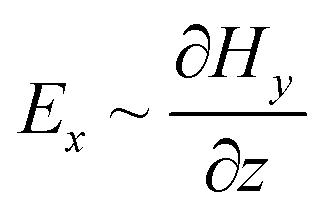 and
and 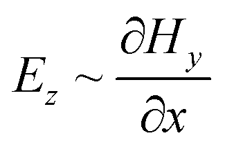 . Clearly, the contribution from |Ez| would deliver some increase of image width in the measure of Ex2 + Ez2, for near field lithography and super lens (Fig. 5(a) and (b)), where |Ex|max/|Ez|max ∼ 2.7 could be seen in the two figures. For the plasmonic cavity lens imaging, great magnitude difference lies between |Ex| and |Ez| components, with |Ex|max/|Ez|max ∼ 10, as a result of surface plasmon coupling inside Ag–Pr–Ag cavity. This point helps to get a narrower image width of plasmonic cavity lens.
3.4 Imaging with multiple nano lines
In this section, the pattern is replaced by multiple nano lines. Fig. 6 shows the electric filed intensities at the centre of photoresist for the plasmonic cavity lens under NI and off-axis illumination (OAI). Here we focus on the imaging behavior for plasmonic cavity lens lithography with NI (Fig. 6(a)), OAI (Fig. 6(b)), and with added grooves adjacent to boundary slits and OAI (Fig. 6(c)). For the imaging with plasmonic cavity lithography under NI (Fig. 6(d)), the double and multiple lines with a 60 nm half-pitch could not be discriminated at an air work distance of 120 nm. This is due to the fact that evanescent waves carrying subwavelength information could not take part in the imaging process. Once off-axis illumination (OAI) with appropriate kx,inc = 1.5k0 is applied to the plasmonic cavity lens, the higher spatial frequency of evanescent wave would participate in the imaging process, and the resolution is enhanced obviously. Meanwhile, the air distance is also elongated to 120 nm. The calculated electric field profiles exhibit well resolved images with a 120 nm air distance as shown in Fig. 6(e), and a longer distance can probably be achieved. This phenomenon, as has been demonstrated in our recent work,41 is mainly attributed to wavevector shifting of evanescent wave components under high spatial frequency spectrum OAI and to the surface plasmon excitations at the interface of the Pr and bottom Ag layer, which enables the reflection enhancement of evanescent waves transmitted through the top Ag layer. However, the proximity effects still exist in the double lines and the multiple lines images (Fig. 6(e)), where the two lines at the boundary show much wider images. Furthermore, upon assist-grooves is added to the side of the two edge lines, almost uniform image patterns of the multiple slits are acquired with 120 nm air distance (Fig. 6(f)). In contrast with the case of the double slits and the multiple slits, the grooves produce negative interference with the two edge slits, and present a field-confined spot imaging as clearly seen in Fig. 6(f). The Fig. 6(g) and (h) plot the electric field profiles at the central of Pr layer for different imaging configuration.They show that the FWHM of the double lines and the multiple lines is remarkably reduced from 110 nm to 80 nm, and 105 nm to 80 nm, respectively, by mounting grooves at the exit side of mask.
The method for the resolution enhancement and proximity correction could be extended to two dimensional cases as well. Fig. 7 shows the simulated results regarding the electric filed intensity for the two-dimensional L-shaped nano lines pattern without or with grooves under OAI plasmonic lithography with 120 nm work distance. As shown clearly in the top row (Fig. 7(a)–(c)), the electric filed intensity is subject to a considerable proximity effect. Instead, by adding the assistant grooves, the proximity effects of two-dimensional patterns are relieved and the profile uniformity of multiple nano-lines is improved considerably (Fig. 7(d)–(f)).
3.5 Lithography experimental results
To demonstrate the above investigations, plasmonic cavity lens imaging lithography experiment was performed in three cases with variant light illumination, proximity correction by grooves, as shown in Fig. 8. Three mask patterns are used here with 1, 2 and 5 nano slits, corresponding to the three columns of Fig. 8. On the top row of Fig. 8 is the plasmonic cavity lens lithography under NI without grooves (Fig. 8(a)–(c)), where the double lines and the multiple lines with 60 nm half-pitch could not be discerned at a air distance of 120 nm. Meanwhile, the width of a single line image becomes apparently broadened, almost reaching 250 nm. This is proved by theoretical simulation in Fig. 3. As high spatial frequency spectrum OAI (kx,inc = 1.5k0) is applied to the plasmonic cavity lens lithography by plane wave vertically impinging on the upside-down isosceles trapeze sapphire prism under a 365 nm mercury lamp illuminating system, the double and multiple lines patterns could be well resolved with a 120 nm air distance, as shown in the middle row of Fig. 8. It is because the higher spatial frequency of evanescent wave would participate in the imaging process, and the resolution is enhanced. However, the proximity effect of a single line, a pair of lines and multiple nano-lines in this case is obvious (Figs. 8(d)–(f)). The line image width for the single slit and double slits are 185 and 115 nm, respectively, much larger than that of mask pattern. Also there are great width difference between two boundary lines and lines inside. As introducing the assistant groove around the edge of object patterns, the width of single, double lines and multiple lines pattern is manifestly controlled and the uniformity is significantly improved under large working distances. Especially the pattern width of the single line case is reduced from 185 nm to 105 nm (Fig. 8(d) and (g)). The pattern width of double nano-lines and multiple nano-lines are also restrained from 115 nm to 82 nm (Fig. 8(e) and (h)) and from 110 nm to 78 nm (Fig. 8(f) and (i)), respectively. This agrees well with the theoretical simulation. | ||
| Fig. 8 SEM images resist patterns for a single line, a pair of lines, multiple lines with air distances of 120 nm under NI and OAI. The top row (a–c) represent to the plasmonic cavity lens lithography under NI. (d–f) and (g–i) in the middle and bottom row represent corresponds to the plasmonic cavity lens lithography without and with groove-assisted resist patterns under OAI, respectively (scale bar, 100 nm). | ||
Although the lines resist pattern is clearly discriminated, great line edge roughness is obvious in Fig. 8. This deleterious feature is believed to be related with Ag film roughness, finite resolution of PR, and even developing process. We will address this point in details and improve pattern quality in later work. In addition, the proximity effect is just corrected with uniform line width in this paper. Some other proximity effect, like rounding of patterns, shortened length etc., could be corrected in the similar way.
4. Conclusions
It has been proposed and demonstrated that imaging resolution and air distance of isolated nano-lines can be significantly improved by applying the plasmonic cavity lens structure, peripheral grooves and off-axis illumination. Our experiments demonstrate that the width of single, double lines and multiple lines pattern is well controlled and the uniformity is significantly improved in lithography with 365 nm light wavelength and 120 nm working distance, being approximately ten times the air distance defined by near field diffraction limit. The proposed approaches will probably lead to potential applications in nanolithography, super-resolution optical microscopy, high-density optical recording etc.Acknowledgements
This work was supported by 973 Program of China (No. 2013CBA01700) and the Chinese Nature Science Grant (61405200, 61575202).Notes and references
- J. Vogelsang, C. Steinhauer, C. Forthmann, I. H. Stein, B. Person-Skegro, T. Cordes and P. Tinnefeld, ChemPhysChem, 2010, 11, 2475–2490 CrossRef CAS PubMed.
- S. Bornfleth and C. Eils, J. Microsc., 1998, 189, 118–136 CrossRef.
- T. Masaki, K. Goto, Y. Inouye and S. Kawata, J. Appl. Phys., 2004, 95, 334–338 CrossRef CAS.
- D. W. Pohl, W. Denk and U. Duerig, Proc. SPIE, 1986, 565, 56–61 CrossRef.
- R. J. Blaikie, D. O. S. Melville and M. M. Alkaisi, Microelectron. Eng., 2006, 83, 723–729 CrossRef CAS.
- T. Ito, T. Yamada, Y. Inao, T. Yamaguchi, N. Mizutani and R. Kuroda, Appl. Phys. Lett., 2006, 89, 033113 CrossRef.
- S. Madsen, N. C. R. Holme, P. S. Ramanujam, S. Hvilsted, J. M. Hvam and S. J. Smith, Ultramicroscopy, 1998, 71, 65–71 CrossRef CAS.
- Y. Kim, H. Jung, S. Kim, J. Jang, J. Y. Lee and J. W. Hahn, Opt. Express, 2011, 19, 19296–19309 CrossRef CAS PubMed.
- J. G. Goodberlet and H. Kavak, Appl. Phys. Lett., 2002, 81, 1315–1317 CrossRef CAS.
- S. Roh, T. Chung and B. Lee, Sensors, 2011, 11, 1565–1588 CrossRef PubMed.
- Y. W. Hao, H. Y. Wang, Z. Y. Zhang, X. L. Zhang, Q. D. Chen and H. B. Sun, J. Phys. Chem. C, 2013, 117, 26734–26739 CAS.
- S. Law, V. Podolskiy and D. Wasserman, Nanophotonics, 2013, 2, 103–130 CrossRef CAS.
- J. D. Caldwell, A. V. Kretinin, Y. Chen, V. Giannini, M. M. Fogler, Y. Francescato, C. T. Ellis, J. G. Tischler, C. R. Woods and A. J. Giles, Physics, 2014, 5, 5221 CAS.
- X. G. Luo, Sci. China: Phys., Mech. Astron., 2015, 58, 1–18 CAS.
- J. B. Pendry, Phys. Rev. Lett., 2000, 85, 3966–3969 CrossRef CAS PubMed.
- Z. Liu, N. Fang, T. J. Yen and X. Zhang, Appl. Phys. Lett., 2003, 83, 5184–5186 CrossRef CAS.
- N. Fang, Z. Liu, T. J. Yen and X. Zhang, Opt. Express, 2003, 11, 682–687 CrossRef CAS PubMed.
- X. Luo and T. Ishihara, Appl. Phys. Lett., 2004, 84, 4780–4782 CrossRef CAS.
- H. Liu, B. Wang, E. S. Leong, P. Yang, Y. Zong, G. Si, J. Teng and S. A. Maier, ACS Nano, 2010, 4, 3139–3146 CrossRef CAS PubMed.
- E. S. Leong, Y. J. Liu, B. Wang and J. Teng, ACS Appl. Mater. Interfaces, 2011, 3, 1148–1153 CAS.
- D. B. Shao and S. C. Chen, Appl. Phys. Lett., 2005, 86, 253107 CrossRef.
- J. Luo, B. Zeng, C. Wang, P. Gao, K. Liu, M. Pu, J. Jin, Z. Zhao, X. Li and H. Yu, Nanoscale, 2015, 7, 18805–18812 RSC.
- S. M. Vukovic, Acta Phys. Pol., A, 2009, 116, 678 CrossRef CAS.
- P. J. Cheng, C. Y. Weng, S. W. Chang, T. R. Lin and C. H. Tien, Opt. Express, 2013, 21, 13479–13491 CrossRef PubMed.
- T. Xu, L. Fang, J. Ma, B. Zeng, Y. Liu, J. Cui, C. Wang, Q. Feng and X. Luo, Appl. Phys. B, 2009, 97, 175–179 CrossRef CAS.
- F. Xu, G. Chen, C. Wang, B. Cao and Y. Lou, Opt. Lett., 2013, 38, 3819–3822 CrossRef CAS PubMed.
- D. Tang, C. Wang, Z. Zhao, Y. Wang, M. Pu, X. Li, P. Gao and X. Luo, Laser Photonics Rev., 2015, 9, 713–719 CrossRef CAS.
- M. Pu, X. Li, X. Ma, Y. Wang, Z. Zhao, C. Wang, C. Hu, P. Gao, C. Huang and H. Ren, Sci. Adv., 2015, 1, e1500396 Search PubMed.
- X. Li, L. Chen, Y. Li, X. Zhang, M. Pu, Z. Zhao, X. Ma, Y. Wang, M. Hong and X. Luo, Sci. Adv., 2016, 2, e1601102 Search PubMed.
- P. Gao, N. Yao, C. Wang, Z. Zhao, Y. Luo, Y. Wang, G. Gao, K. Liu, C. Zhao and X. Luo, Appl. Phys. Lett., 2015, 106, 093110 CrossRef.
- E. Betzig and J. K. Trautman, Science, 1992, 257, 189–195 CAS.
- G. Lerosey, J. D. Rosny, A. Tourin and M. Fink, Science, 2007, 315, 1120–1122 CrossRef CAS PubMed.
- D. Melville and R. Blaikie, Opt. Express, 2005, 13, 2127–2134 CrossRef CAS PubMed.
- N. Fang, H. Lee, C. Sun and X. Zhang, Science, 2005, 308, 534–537 CrossRef CAS PubMed.
- P. Chaturvedi, W. Wu, V. J. Logeeswaran, Z. Yu, M. S. Islam, S. Y. Wang, R. S. Williams and N. X. Fang, Appl. Phys. Lett., 2010, 96, 043102 CrossRef.
- H. Liu, B. Wang, L. Ke, J. Deng, C. C. Chum, S. L. Teo, L. Shen, S. A. Maier and J. Teng, Nano Lett., 2012, 12, 1549–1554 CrossRef CAS PubMed.
- M. D. Arnold and R. J. Blaikie, Opt. Express, 2007, 15, 11542–11552 CrossRef PubMed.
- C. W. Holzwarth, J. E. Foulkes and R. J. Blaikie, Opt. Express, 2011, 19, 17790–17798 CrossRef CAS PubMed.
- C. Wang, P. Gao, Z. Zhao, N. Yao, Y. Wang, L. Liu, K. Liu and X. Luo, Opt. Express, 2013, 21, 20683–20691 CrossRef PubMed.
- L. Hong, W. Bing, K. Lin, D. Jie, C. C. Chan, S. Z. Ming, S. Lu, S. A. Maier and H. T. Jing, Adv. Funct. Mater., 2012, 22, 3777–3783 CrossRef.
- Z. Zhao, Y. Luo, W. Zhang, C. Wang, P. Gao, Y. Wang, M. Pu, N. Yao, C. Zhao and X. Luo, Sci. Rep., 2015, 5, 15320–15330 CrossRef CAS PubMed.
- R. L. Wadsack, Bell Syst. Tech. J., 1978, 57, 1449–1474 CrossRef.
- B. Radisavljevic, M. B. Whitwick and A. Kis, ACS Nano, 2011, 5, 9934–9938 CrossRef CAS PubMed.
- A. A. Houck, H. E. Türeci and J. Koch, Nat. Phys., 2012, 8, 292–299 CrossRef CAS.
- J. W. Silverstone, D. Bonneau, K. Ohira, N. Suzuki, H. Yoshida, N. Iizuka, M. Ezaki, C. M. Natarajan, M. G. Tanner and R. H. Hadfield, Nat. Photonics, 2014, 8, 104–108 CrossRef CAS.
- V. M. Shalaev, W. Cai, U. K. Chettiar, H. K. Yuan, A. K. Sarychev, V. P. Drachev and A. V. Kildishev, Opt. Lett., 2005, 30, 3356–3358 CrossRef PubMed.
- J. Valentine, S. Zhang, T. Zentgraf, E. Ulin-Avila, D. A. Genov, G. Bartal and X. Zhang, Nature, 2008, 455, 376–379 CrossRef CAS PubMed.
- W. Lv, S. Liu, Q. Xia, X. Wu, Y. Shen and E. Y. Lam, J. Vac. Sci. Technol., A, 2013, 31, 041605 Search PubMed.
- M. G. Moharam, T. K. Gaylord, E. B. Grann and D. A. Pommet, J. Opt. Soc. Am. A, 1995, 12, 1068–1076 CrossRef.
- P. Srisungsitthisunti, O. K. Ersoy and X. Xu, Appl. Phys. Lett., 2011, 98, 223106 CrossRef.
- B. Zeng, Y. Zhao, L. Fang, C. Wang and X. Luo, J. Opt. A: Pure Appl. Opt., 2009, 11, 125003–125007 CrossRef.
Footnotes |
| † Electronic supplementary information (ESI) available. See DOI: 10.1039/c7ra00116a |
| ‡ These authors contributed equally to this work. |
| This journal is © The Royal Society of Chemistry 2017 |