
 Open Access Article
 This Open Access Article is licensed under a
 Creative Commons Attribution 3.0 Unported Licence
Viable approach toward efficient p-type conductivity in Al-doped anatase TiO2 via strain engineering†
Wei Zhou ab and
Naoto Umezawa*b
ab and
Naoto Umezawa*b
aDepartment of Applied Physics, Tianjin Key Laboratory of Low Dimensional Materials Physics and Preparing Technology, Faculty of Science, Tianjin University, Tianjin 300072, People's Republic of China. E-mail: weizhou@tju.edu.cn
bInternational Center for Materials Nanoarchitectonics (MANA), National Institute for Materials Science, 1-1, Namiki, Tsukuba, Ibaraki 305-0044, Japan. E-mail: UMEZAWA.Naoto@nims.go.jp
First published on 10th April 2017
Abstract
Realization of efficient p-type conductivity in wide gap oxides is a challenging task partly due to the localized nature of non-bonding oxygen 2p states of which the valence band maximum consists. In this study, effects of anisotropic strain on an accepter level of Al-doped anatase TiO2 are investigated using LDA+U calculations. Strain engineering effectively increases the cation states in the valence band maximum of TiO2. It is demonstrated that a deep acceptor level induced by substitutional Al for Ti is turned into a delocalized shallow level under a tensile strain of as much as 8%. This effect is confirmed by the analysis of thermodynamic transition level which is largely shifted from 0.8 eV above to below the valence band maximum, being a shallow acceptor, as the tensile strain is increased.
Introduction
Anatase TiO2, known as a wide-gap oxide semiconductor, is widely used in electronics, lithium-ion batteries, as well as photonic and photochemistry applications due to its excellent physical and chemical properties.1–5 For examples, Hitosugi and Hasegawa et al. have proposed Nb doped TiO2 as a good candidate for n-type transparent conductive oxides.6–8 Meanwhile, after the discovery of the photo-induced water splitting on a TiO2 electrode by Fujishima et al., anatase TiO2 has been extensively studied as a promising photocatalyst material.9 For these potential applications, the controllability of the carrier concentration, transportation and recombination in anatase TiO2 are of great interest. However, most of the previous studies indicate that the anatase TiO2 exhibits unintentional n-type conductivity, while a stable p-type conductivity is difficult to obtain.10,11 Therefore, the preparation of TiO2 with good p-type conductivity is especially important for photoelectron and photochemistry applications.Recently, one possible origin for poor p-type conductivity of wide band gap oxides was proposed that the introduced holes will be trapped as polarons in the crystal.12 It is known that the valence band maximum (VBM) of most oxides is derived from non-bonding O 2p orbitals, which possess localized nature. Thus, when the holes are created by p-type doping with extrinsic elements, they will be trapped by O 2p orbitals to form stable polarons with low mobility resulting in the poor p-type conductivity. Experimentally, self-trapped holes in TiO2 have been observed from electron paramagnetic resonance (EPR) and photoluminescence (PL) measurements.13,14 The density functional theory (DFT) calculations with band gap corrections, such as DFT+U or hybrid functional, further suggested that holes in TiO2 are trapped at deep acceptor levels,12,15,16 contrary to the results from standard DFT calculations.
Since the holes in anatase TiO2 act as self-trapped polarons, it is crucial to delocalize the trapped holes by modifying the electronic structure for the realization of viable p-type conductivity. Recently, strain engineering has been considered as an effective approach to change the electronic structure of materials. Especially, some reports have pointed out that the electrical conductivity behavior of oxides can be controlled by the external strain.17,18 Meanwhile, Hosono et al. have given a principle for designing p-type materials with increasing the contribution of cation orbitals in the VBM by choosing constituents of materials, called “chemical modulation of the valence band”.19 It was firstly proposed for successfully predicting a new p-type oxide compound of CuAlO2. They pointed out that Cu 3d–O 2p mixing in the valence band mediated a small ionization potential, promoted an increased valence band dispersion, and favoured p-type conductivity. The above principle can also be applicable to general oxides if one can increase the contribution of cation orbitals at the VBM by external perturbation. The strain engineering is a promising approach for this purpose and is useful for the design of novel p-type oxide semiconductors. However, the corresponding investigations on the wide band gap oxides which play important roles in industry, such as TiO2, have not been systematically explored in elsewhere yet.
In this work, effects of anisotropic strain on the capability of substitutional Al at Ti sites (AlTi) for hole doping in anatase TiO2 are studied using the local density approximation plus on-site Coulomb interaction U approach (LDA+U). Al was chosen as the doping element to generate holes in this work, since it is known as a typical acceptor in TiO2 and its doping process has been established experimentally.20 Our calculations indicate that the tensile strain in the (001) plane can effectively delocalize hole carriers associated with Al doping along with band gap narrowing in TiO2. Moreover, the shallow acceptor level was obtained from increasing the contribution of Ti 3d orbital at VBM with the tensile strain, which offers a viable way to realize the efficient p-type conductivity in oxide compounds.
Methodology
All spin polarized calculations here were performed with the Vienna Ab initio Simulation Package (VASP) based on the density functional theory (DFT).21 The projector-augmented wave (PAW) was used for the electron–ion interactions. The local density approximation plus onsite Coulomb interaction U was adopted for the exchange–correlation energy functional.22,23 The U was applied to both Ti 3d and O 2p states following the scheme suggested in ref. 24. The number of k points and the cutoff energy were increased until the calculated total energy converged within an error of 1 × 10⁻⁵ eV per atom. Therefore, the cut-off energy of 500 eV with 3 × 3 × 4 k points was set for a 3 × 3 × 1 supercell with 96 atoms extended from a relaxed six-atom primitive cell of anatase TiO2. For the Brillouin-zone integration, the tetrahedron method was used. Since the electron occupies the state in order of energy with the fixed occupation of one, the integration of states to the total electron number gives the highest occupied state. The energy convergence tolerance was set to below 5 × 10⁻⁶ eV per atom. The lattice vectors and atomic coordinates were relaxed until the Hellmann–Feynman force on each atom is reduced to less than 0.01 eV Å−1. The structural model of anatase TiO2 was shown in Fig. 1(a). To simulate the biaxial strain in the (001) plane, the relaxation of crystal with the lattice constants a and b fixed was performed until the stress along c axis was free. And the specified in-plane strain was defined as ε = (a − a0)/a0, where a is a new lattice parameter and a0 is the lattice parameter for un-strained structure.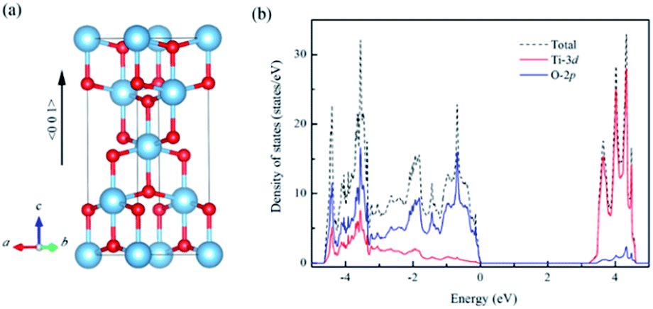 | ||
| Fig. 1 (a) Crystal structure of anatase TiO2. (b) The calculated density of states for un-doped anatase TiO2 (the energy range is referenced to the value of the highest occupied state (VBM)) (blue ball: Ti, red ball: O). | ||
It is known that the standard local or semi-local density functionals are subject to self-interactions that are the major source of the underestimation of the band gap in semiconductor materials. To counteract this problem, the local density approximation with on-site Hubbard corrections was applied to both Ti 3d and O 2p orbitals. The values of U were determined from single ions, and exported to bulk anatase TiO2 with a multiplied parameter fitted for an experimental band gap (U = 7.51 eV for Ti 3d and U = 4.37 eV for O 2p).24 Since the 3s and 3p orbitals of Al are less localized, U correction was not applied. This treatment is justified by our hybrid density functional calculations for projected density of states of Al-doped TiO2, which confirm the delocalized Al states and exhibit essentially the same electronic structures as our LDA+U calculations near the band edges as shown in Fig. S2.† Interestingly, this setting can well reproduce lattice constants and intrinsic electronic structure of anatase TiO2 as shown below.
Results and discussion
For un-doped anatase TiO2 crystal, the calculated lattice constants from LDA+U are a = 3.89 Å and c = 9.52 Å, which are much close to the previous experimental and theoretical results.25,26 As for the band gap, the calculated value increases from 1.89 eV of LDA to 3.16 eV of LDA+U which also gives a good agreement with the experimental optical band gap (3.2 eV).27 This indicates that U values used here are moderate choice for accurate estimation of both the lattice constants and band gap of TiO2. Then, the calculated density of states (DOS) of un-doped TiO2 is plotted in Fig. 1(b). It shows that the maximum of valence band is mainly consist of O 2p states, while the minimum of conduction band (CBM) is contributed by Ti 3d states. These are consistent with previous theoretical reports.24 It is known that hole carriers are hardly delocalized in anatase TiO2 because of the pronounced contribution of localized O 2p states in the valence band. As for the Al doping case, it does not significantly change the character of VBM and CBM in anatase TiO2. The VBM is still dominated by the O 2p orbitals. Besides, an isolate unoccupied state (acceptor state) forms in the band gap with 0.4 eV higher than the highest occupied state as shown in Fig. 2(a). This acceptor state is relatively deep and mainly originates from the hole states of O 2p due to the lower oxidation number of Al compared with Ti.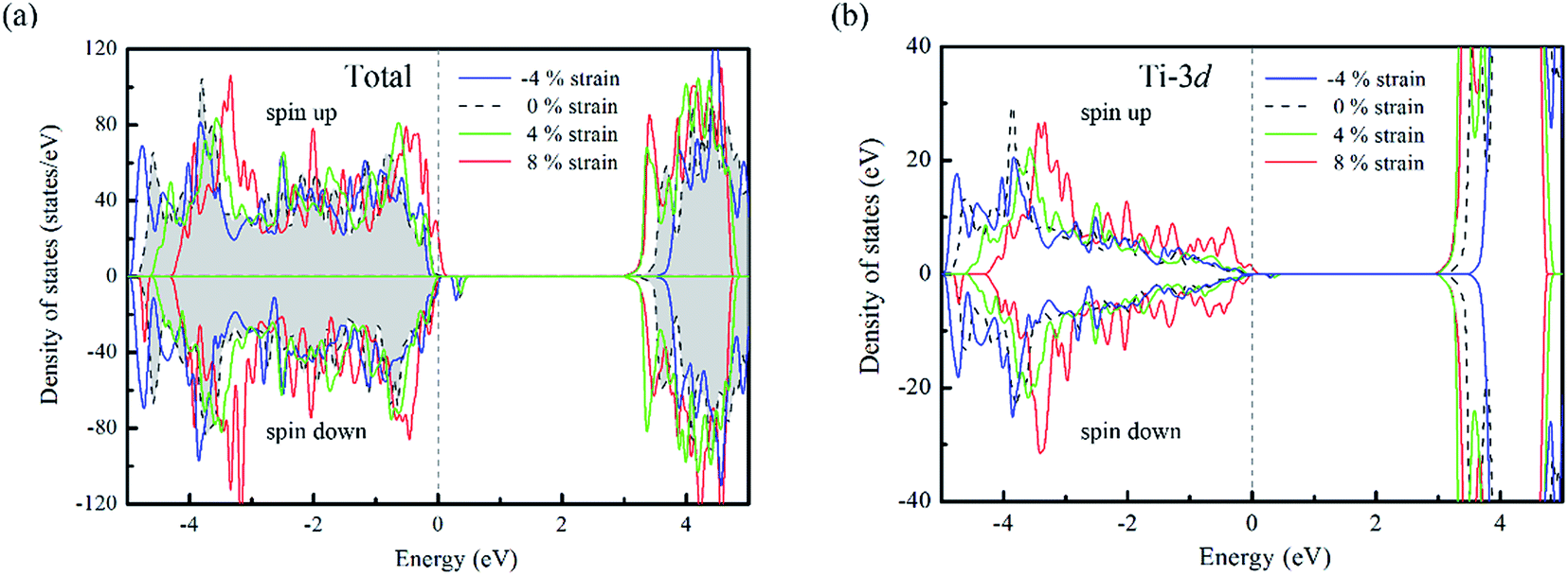 | ||
| Fig. 2 (a) The calculated total density of states and (b) partial density of states for Ti atoms in Al doped TiO2 with biaxial strain (the energy range is referenced to the value of the highest occupied state). | ||
Since the hole-trapping of wide band gap oxide is considered to originate from the localized O 2p states dominating at the VBM, one possible way to delocalize the holes in TiO2 is increasing the contribution of cation orbitals in the valance band by strengthening interactions between O and Ti atoms. Strain engineering has been thought as a viable approach to modify the chemical bonding of materials. Meanwhile, the biaxial strain usually exists in experiments, such as during the epitaxial thin film growth. Therefore, taking into account the 〈001〉 direction is the soft axis of TiO2 crystal,28 the biaxial stain in the (001) plane was imposed to modify the orbital composition in valance band of Al-doped TiO2.
From the DOS of Fig. 2(a), we noticed that the imposed biaxial strain can obviously change the electronic structure of Al-doped TiO2 system, such as the position of the acceptor level. When the tensile strain amplitude is smaller than 8%, the formed acceptor state still exists in the band gap as an isolated energy level away from the valence band. After the tensile strain approaching to 8%, the deep acceptor state disappears from the band gap providing a free hole carrier at the top of valence band, which thus results in a p-type conductivity. This mainly originates from enhanced Ti 3d character at the top of the valence band (Fig. 2(b)), which promotes hybridization of O 2p non-bonding states with the Ti 3d states. To understand more about the nature of the acceptor level under the strain, the charge density corresponding to the unoccupied acceptor state (hole state) introduced by Al doping is depicted in Fig. 3. For the un-strained model, the hole states introduced by substituting Al for Ti are mainly trapped by the first neighboring oxygen atoms, implying the localized character of the acceptor states. While in the structure with 8% biaxial tensile strain, it clearly exhibits that the hole carrier is delocalized and extended over the whole space of crystal. That is to say, the introduced holes can freely migrate through O 2p orbitals. Additionally, the delocalization of holes will discourage the formation of photo-generated carrier recombination centers originating from self-trapped holes at oxygen non-bonding states, which is beneficial for enhancing its photocatalytic performance. This is similar with the case of Ti-defected TiO2 reported by Wang et al.29
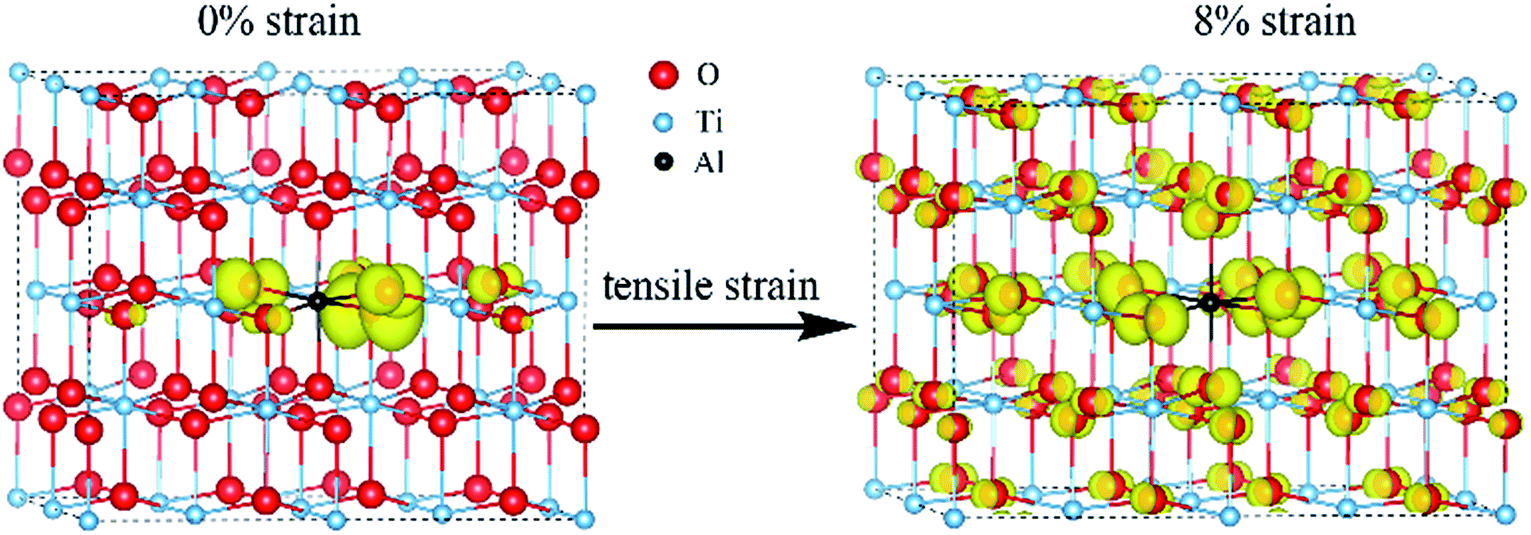 | ||
| Fig. 3 The charge density of hole states in Al doped TiO2 without and with 8% biaxial tensile strain (the isosurface is set to 0.003 e Å−3). | ||
To further analyze the nature of acceptor states in Al-doped TiO2, the formation energy for the substitutional Al for Ti with charge state q was calculated from the formula:30
 | (1) |
 | ||
| Fig. 4 The calculated formation energy and transition level for Al-doped anatase TiO2 with different biaxial strains at oxygen-rich condition (the origin of the Fermi level is set at the VBM). | ||
When the biaxial tensile strain is applied to the Al-doped TiO2 crystal, the transition level of ε(0/−1) gradually shifts downwards and enters into the valence band. Eventually AlTi−1 predominates in the entire range of the Fermi energy in the band gap when the tensile strain reaches as much as 8%. It indicates AlTi becomes a shallow acceptor in TiO2 with 8% biaxial tensile strain. Since AlTi is negatively ionized even when the Fermi level is very close to the VBM, it is considered to provide free hole carriers as a counter charge, leading to a p-type conductivity. On the other hand, it is known that the oxygen vacancies usually form as unintentional donors and compensate hole carriers induced by the acceptor doping in oxides. Since the Al substituting Ti acts as an acceptor to produce holes in the TiO2, the generation of oxygen vacancies, which provide electrons to compensate holes, is expected for the formation of the closed shell electronic structure. Thus, we consider the formation energy of an oxygen vacancy with its doubly positive charge state using the formula eqn (1) to investigate its relative stability with respect to singly negative AlTi as shown in Fig. 4. Here we take into account only +2 charge state of VO, because it is the predominant charge state and relevant to the Femi level position of our system.15,31 The pinned Fermi level corresponds to the intersection of the two lines for  (AlTi−1) and
  (VO2+), at which the charge neutrality of the system is nearly satisfied.32 It is observed that the pinned Fermi level is gradually shifted downwards with increasing the biaxial tensile strain. This originates from the fact that the formation energy of
  increases while that of
  decreases upon tensile strain, leading to the downward shift of the pinned Fermi level. This clearly indicates that the tensile strain is beneficial for avoiding the compensation effect of oxygen vacancy. This result further confirms that the tensile strain in the (001) plane is a viable way to realize the p-type conductivity in Al-doped TiO2.
We turn now to the issue of the possible origin for the delocalization of trapped holes. Before discussion, it is noticed that the Al doping do not significantly modify the band edge electronic structures because of much lower content of Al sp states than that of Ti 3d states as shown in Fig. S1.† Thus, we ignored their contributions to the band edge character in the following discussion. Since the cation orbitals at VBM play key roles in breaking the localization of positive holes, the distribution of Ti 3d orbital in different strained structures was analyzed. It is known that anatase TiO2 is constituted with the TiO6 octahedra units, and the apical axes with a longer Ti–O bond length are along the [001] direction of crystal. Thus, the anisotropy orbital contribution due to the crystal symmetry can be expected. From the orbital projected band structure in Fig. 5(a), the contributions of cation states at the VBM of un-doped TiO2 are dominated by the Ti 3dxz and Ti 3dyz orbitals. It implies that the orbital component of cation atoms (Ti) at the VBM is more sensitive to the bonding interactions along the 〈001〉 direction. When the biaxial tensile strain is imposed into the (001) plane of Al doped TiO2, the Ti–O bond length along 〈001〉 axis is dramatically shortened reflecting Poisson's ratio as shown in the inset of Fig. 5(b). Meanwhile, the Al doping further decreases the Ti–O bond length because of the shrink of crystal volume from small ionic size of Al dopant. As a consequence, the interaction between Ti and O atoms will be enhanced. This change is also confirmed by the charge population analysis. The calculated Bader charge of Ti atom is enlarged from +2.0e to +2.2e when the 8% tensile strain is stressed into the relaxed structure. It indicates the covalent bond of Ti–O actually becomes stronger in the tensile strained model. Then, the strengthened hybridization between Ti and O atoms increases the contribution of Ti 3d states at VBM, which can be clearly seen in the Fig. 2(b) and 5(b). With the above analysis, we can propose that the pronounced Ti 3d contribution at the VBM due to decreasing the Ti–O bond length along the 〈001〉 direction. Therefore, the anisotropic strain can effectively delocalize the trapped holes on oxygen site in Al doped TiO2 crystal.
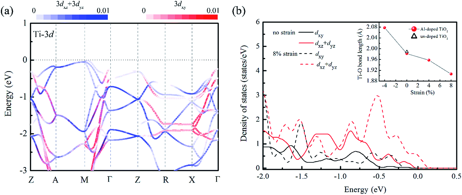 | ||
| Fig. 5 (a) Orbital-projected band structure of pure TiO2 (the scale indicates the magnitude of the projection), (b) the projected density of states for Al-doped TiO2 under different strain conditions, and the inset is the calculated Ti–O bond length (the energy range is referenced to the value of the highest occupied state). | ||
Conclusions
In conclusion, the LDA with on-site Coulomb interaction U applied to both Ti 3d and O 2p orbital was adopted to study the capability of substitutional Al for Ti as an effective acceptor in anatase TiO2 from strain engineering. In an un-strained crystal, AlTi is characterized by the formation of strongly localized holes in consistent with the experimental results. After biaxial strain imposed into the crystal, our calculations indicate that only the tensile strain in the (001) plane can effectively delocalize the trapped holes in anatase TiO2, which comes from the enhanced contribution of Ti 3d orbital at VBM. This is extremely valuable for photochemical applications, such as photocatalysis, because the enhanced delocalization ability for holes can improve the hole-carrier transfer and discourage the formation of photo-generated carrier recombination centers originating from self-trapped holes at oxygen non-bonding states to increase the photocatalysis efficiency. More importantly, our studies give a viable way to realize the effective p-type conductivity in oxide compounds from strain engineering.Acknowledgements
We thank Professor J. Ye and Professor P. Wu for useful discussions. This work is partly supported by the Japan Science and Technology Agency (JST) Precursory Research for Embryonic Science and Technology (PRESTO) program and by the World Premier International Research Center Initiative on Materials Nanoarchitectonics (MANA), MEXT.Notes and references
- A. L. Linsebigler, G. Lu and J. T. Yates Jr, Chem. Rev., 1995, 95, 735 CrossRef CAS.
- A. Fujishima, X. Zhang and D. A. Tryk, Surf. Sci. Rep., 2008, 63, 515 CrossRef CAS.
- A. J. Cowan and J. R. Durrant, Chem. Soc. Rev., 2013, 42, 2281 RSC.
- H. Lyu, J. Liu, S. Qiu, Y. Cao, C. Hu, S. Guo and Z. Guo, J. Mater. Chem. A, 2016, 4, 9881 CAS.
- X. Su, Q. Wu, X. Zhan, J. Wu, S. Wei and Z. Guo, J. Mater. Sci., 2012, 47, 2519 CrossRef CAS.
- T. Hitosugi, Y. Yamamoto and K. Inaba, Appl. Phys. Lett., 2005, 86, 252101 CrossRef.
- T. Hitosugi, A. Ueda, S. Nakao and N. Yamada, Appl. Phys. Lett., 2007, 90, 212106 CrossRef.
- N. Yamada, T. Hitosugi, J. Kasal, N. L. H. Hoang, S. Nakao, Y. Hirose, T. Shimada and T. Hasegawa, Thin Solid Films, 2010, 518, 3101–3104 CrossRef CAS.
- A. Fujishima and K. Honda, Nature, 1972, 238, 37–38 CrossRef CAS PubMed.
- T. Miyagi, M. Kamei, I. Sakaguchi, T. Misuhashi and A. Yamzaki, Jpn. J. Appl. Phys., 2004, 43, 775–778 CrossRef CAS.
- J. Biedrzychi, S. Livraghi, E. Giamello, S. Agnoli and G. Granozzi, J. Phys. Chem. C, 2014, 118, 8462–8473 Search PubMed.
- J. B. Varley, A. Janotti, C. Franchini and C. G. Van de Walle, Phys. Rev. B: Condens. Matter Mater. Phys., 2012, 85, 081109 CrossRef.
- S. Yang, A. T. Brant and L. E. Halliburton, Phys. Rev. B: Condens. Matter Mater. Phys., 2010, 82, 035209 CrossRef.
- H. Tang, H. Berger, P. E. Schmid and F. Lévy, Solid State Commun., 1993, 87, 847–851 CrossRef CAS.
- B. J. Morgan and G. W. Watson, Phys. Rev. B: Condens. Matter Mater. Phys., 2009, 80, 233102 CrossRef.
- P. Deák, B. Aradi and T. Frauenheim, Phys. Rev. B: Condens. Matter Mater. Phys., 2011, 83, 15520 CrossRef.
- S. Nakao, N. Yamada, Y. Hirose and T. Hasegawa, Appl. Phys. Express, 2012, 5, 061201 CrossRef.
- A. Janotti, D. Steiauf and C. G. Van de Walle, Phys. Rev. B: Condens. Matter Mater. Phys., 2011, 84, 201304 CrossRef.
- H. Kawazoe, H. Yanagi, K. Ueda and H. Hosono, MRS Bull., 2000, 25, 28 CrossRef CAS.
- S. Das, D. Liu, J. Park and Y. Hahn, J. Alloys Compd., 2013, 553, 188 CrossRef CAS.
- G. Kresse and J. Hafner, Comput. Mater. Sci., 1996, 6, 15–50 CrossRef CAS.
- V. I. Anisimov, F. Aryasetiawan and A. I. Lichtenstein, J. Phys.: Condens. Matter, 1997, 9, 767–808 CrossRef CAS.
- S. L. Dudarev, G. A. Botton, S. Y. Savrasov, C. J. Humphreys and A. P. Sutton, Phys. Rev. B: Condens. Matter Mater. Phys., 1998, 57, 1505 CrossRef CAS.
- N. Umezawa and J. H. Ye, Phys. Chem. Chem. Phys., 2012, 14, 5924–5934 RSC.
- J. K. Burdett, T. Hughbanks, G. J. Miller, J. W. Richardson Jr and J. V. Smith, J. Am. Chem. Soc., 1987, 109, 3639–3946 CrossRef CAS.
- F. Tielens, M. Calatayud, A. Beltran, C. Minot and J. Andres, J. Electroanal. Chem., 2005, 581, 216–223 CrossRef CAS.
- H. Sun, D. J. Mowbray, A. Migani, J. Zhao, H. Petek and A. Rubio, ACS Catal., 2015, 5, 4242 CrossRef CAS.
- W. J. Yin, S. Y. Chen, J. H. Yang, X. G. Gong, Y. F. Yan and S. H. Wei, Appl. Phys. Lett., 2010, 96, 221901 CrossRef.
- S. Wang, L. Pan, J. Song, W. Mi, J. Zou, L. Wang and X. Zhang, J. Am. Chem. Soc., 2015, 137, 2975 CrossRef CAS PubMed.
- D. O. Scanlon and G. W. Watson, J. Mater. Chem., 2012, 22, 25236 RSC.
- A. Boonchun, P. Reunchan and N. Umezawa, Phys. Chem. Chem. Phys., 2016, 18, 30040 RSC.
- A. Peles and C. G. Van de Walle, Phys. Rev. B: Condens. Matter Mater. Phys., 2007, 76, 214101 CrossRef.
Footnote |
| † Electronic supplementary information (ESI) available. See DOI: 10.1039/c6ra28878b |
| This journal is © The Royal Society of Chemistry 2017 |