
 Open Access Article
 This Open Access Article is licensed under a
 Creative Commons Attribution 3.0 Unported Licence
Multiscale structured germanium nanoripples as templates for bioactive surfaces†
Rossana Dell'Anna‡
 *a,
Cecilia Masciullo‡b,
Erica Iacoba,
Mario Barozzia,
Damiano Giubertonia,
Roman Böttgerc,
Marco Cecchinib and
Giancarlo Pepponia
*a,
Cecilia Masciullo‡b,
Erica Iacoba,
Mario Barozzia,
Damiano Giubertonia,
Roman Böttgerc,
Marco Cecchinib and
Giancarlo Pepponia
aFondazione Bruno Kessler, Centre for Materials and Microsystems, Micro Nano Facility, Via Sommarive 18, 38123 Trento, Italy. E-mail: dellanna@fbk.eu
bNEST, Scuola Normale Superiore and Istituto Nanoscienze-CNR, Piazza San Silvestro 12, 56127 Pisa, Italy
cHelmholtz-Zentrum Dresden-Rossendorf, Institute of Ion Beam Physics and Materials Research, Bautzner Landstraße 400, 01328 Dresden, Germany
First published on 30th January 2017
Abstract
Nanostructured germanium substrates are produced by gold ion implantation; they show periodic ripples of nanometer size, decorated on the top and partially on one side with a forest of curled nanowires that end with gold-rich nanoparticles. For the first time, through a novel two-step soft lithography transfer process, the multi-scale nanopatterns are replicated, with features well below 100 nm, on biocompatible 2-norbornene ethylene cyclic olefin copolymer substrates. Given the suitable aspect ratio of the nanoripples and the peculiarity of their multiscale structure, the final substrates are available for cell–material interaction studies that can shed light on the role of the hierarchy of nanostructured materials in controlling the large-scale cellular behavior on biocompatible scaffolds. This work also presents an original combination of numerical analyses of scanning force microscopy images, which allows an accurate quantitative description of the outputs of the two-step transfer process.
1. Introduction
Ion beam bombardment at a few tens of keV energy can lead to the spontaneous formation of periodic ripples or dot nanopatterns on the surface of semiconductors, metals and insulators.1 As a single-step method to fabricate regular patterns over large surface areas, it can potentially overcome the limits of conventional lithographic methods, when nanometric features and high-throughput production capability are required;2 hence, ion beam induced nanopattern formation has been investigated for different applications, such as electronic3-and bio-devices.4 To date, a comprehensive theoretical description of all the mechanisms governing the ripple and dot formation is still under debate. According to the Bradley and Harper theory5 and its non-linear generalization for the long time limit,6 the self-organized pattern formation is the product of a competition between a curvature-dependent roughening instability by surface sputtering, and a surface smoothening process by thermal diffusion or other relaxation mechanisms.7,8 The experimental works have highlighted the dependence of the nanopattern characteristics on various parameters, such as the ion beam energy, incident angle, dose and species, as well as the sample temperature. Despite the theoretical progress made so far, it is still difficult to directly correlate all the diverse nanopattern features, achievable by tuning the experimental parameters, to the numerical parameters used in the theories describing the physical mechanism.9 Therefore, the production of nanostructures for specific applications still relies on semi-empirical choices of the ion beam parameters and sample properties.10A peculiar phenomenon develops when the surface of germanium and other III–V semiconductors is irradiated at room temperature with heavy ions11 (Mn+ being the lower mass ion reported12), with energy spanning from few tens of keV to MeV and a fluence in the range of about 1015 to 1017 ions per cm2. Nanometric voids are formed in the amorphized material and, depending on the primary ion energy, irregular porous structures11 or hexagonally ordered nano-holes13 can be induced, both with a mean diameter of the order of 50 nm or less. It was also shown that nanodot-like surface patterns first, and nanohole-like surface patterns afterwards, can evolve with the ion energy into a sponge-like morphology.14 The Ge nanovoid formation was first reported by I. H. Wilson et al.,15 and more recently it has been discussed also for ion implantation at lower energy.13,14 The developed patterns do not match those predicted by the curvature dependent erosive instability, and are instead a specific phenomenon of germanium and other III–V semiconductors.9 They are thought to depend on vacancy accumulation and clustering, forming voids at variable depth in the amorphous layer, and, for specific energy ranges, close enough to the irradiated surface to be later (i.e. with the increasing ion dose) exposed by surface erosion.14 In the microelectronics industry, germanium has recently drawn renewed attention for high-performance devices, because of its intrinsic high electron and hole mobility, smaller band-gap and lower process temperature as compared with silicon. The combination of its semiconductor properties with the pore characteristics, such as the pore geometry, the large surface to volume ratio and the possibility of hosting metal nanoparticles, allows in principle the engineering of this material for optoelectronics, and photovoltaic applications.16 In addition, the sponge-like structure could be relevant for filters,17 gas sensors,18 and thermoelectric materials.19,20
The possibility of a multiscale structuring of a germanium surface by ion implantation, aimed at merging into a single step self-organized ripple patterns of a few hundred nanometer periods, and sponge-like structures of a few ten nanometer size that lie mainly on the ripple crests, is new and envisages its importance in various applications of advanced functional surfaces. In this work, this kind of multiscale topology was obtained by bombarding a Ge surface with Au+ ions, following a recipe first reported by Mollick et al.21 Cross-section transmission electron microscopy (TEM) (ESI,† Fig. S1) has shown the presence of nanowires on the top of the ripples, forming a sponge-like structure, ending in gold-rich nanoparticles, as shown by the joint EDX analysis (data not shown).
Different possible applications of this hierarchical structure can be envisaged. Here it is only mentioned that, in nanoporous semiconductors, the presence of periodic patterns has been shown to be promising for tuning optical properties22 and thermoelectric properties.23 In addition, the periodicity of the ripples ensures a periodic spatial distribution of the Au nanoparticles that could in principle be used for those applications related to in-plane biaxial optical anisotropy, such as a polarization sensitive localized plasmon surface resonance.24–26 In this perspective, the possibility of aligning the metal particles on the top of the crests in conjunction with the ion beam irradiation step, and not after the fabrication of the ripple template on the substrate, constitutes a valuable step forward towards the large-scale integration of semiconductor and plasmonic devices.
This communication reports a completely different technological use of the obtained multiscale nanopatterned germanium substrates, namely a fabrication process of bioactive surfaces for regenerative applications. The structure–function relationship of many biomaterials often depends on their hierarchical structure.27 An example is provided by the extracellular matrix (ECM), which forms the natural cell scaffold and the main extracellular tissue component. Via the mechanotransduction mechanism, the mechanical forces provided by the ECM multiscale topography induce cellular responses, which in turn modulate changes to cell morphology and function.28 Recent studies29,30 have shown that cells alter their phenotype in response to ECM topographical features on different scales, ranging from nano to micron sizes. The design of biomaterials for tissue regeneration aims to fabricate scaffolds that mimic some specific ECM environment characteristics, gaining control over the desired cell response.30
For example, in the field of neural regenerative medicine, adhesion, polarization and migration properties of neuronal cells driven by contact interaction with artificial cues of biocompatible plastic substrates have been largely studied.28,31–35 Rigid silicon molds with alternating lines of ridges and grooves (periodicity ≥ 1 μm, groove depth between 250 nm and 500 nm) were fabricated by electron beam lithography and dry etching techniques, and the patterns were then transferred in a reproducible way onto a thermoplastic material, the copolymer 2-norbornene ethylene cyclic olefin copolymer (COC), by thermal nanoimprinting lithography (NIL). “Ideal” nanogratings (NGs) as well as NGs with controlled degrees of random topographical noise were fabricated. The structures resulted capable of tuning cellular mechanotransduction, in terms of neurite alignment and focal adhesions development, while the loss of neurite alignment showed a threshold response to the level of noise, with cells able to successfully retrieve the NG topography for up to about 50% of the randomly reduced surface directionality.28 It is particularly remarkable that in these studies no surface functionalization was required.
To further help the rational engineering of scaffolds for, but not limited to, the regeneration of the nervous system, smaller spatial scales of cell–ECM topography interaction is one of the possibilities to be investigated. To this aim, the self-organized periodic ripple nanopatterns with the superimposed nanowired structure obtained by ion irradiation have been used in a new two-step pattern-transfer process, producing a final replica onto a COC substrate. This result allows the investigation of the mechanotransduction from artificial regular geometries characterized by a periodicity of about 300 nm, which considerably reduced the value of 1 μm or greater previously considered.28,31
Furthermore, the presence on the ripples of the thermoplastic substrate of what has been reproduced of the original nanowired morphology (of an initial average height of about 90 nm) can contribute to the biological study of the interplay between features of different nano-size in modulating the cellular response to topographic cues. This can cast light on the role of the hierarchy of nanostructured materials in controlling the large-scale cellular behavior on biocompatible scaffolds.29 The production of the nanostructured germanium by Au+ implantation is an expensive process, in terms both of the time and the infrastructure needed. Accordingly, the two-steps transfer process was designed to preserve the fragile original germanium substrate by fabricating in a short time one or more low-cost intermediate perfluoropolyether (PFPE) molds. The intermediate mold was then used in a thermal NIL process to transfer the original nanopatterns onto many (up to tens) final biocompatible COC replicas. Fig. 1 outlines the two-step transfer process.
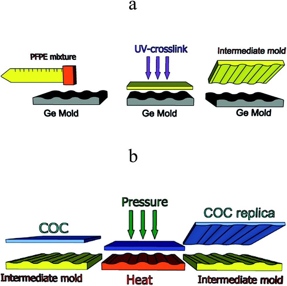 | ||
| Fig. 1 A sketch of the two-step transfer process. (a) The UV-crosslinking process, producing the PFPE intermediate mold starting from the germanium mold, nanostructured by Au+ irradiation. For readability reasons, simple non-structured nanoripples are shown; (b) the thermal NIL process, producing the final COC replica of the nanowired ripples. More details are provided in Section 2.2. | ||
To the authors' knowledge, this is the first case in which a substrate nanopatterned by ion beam irradiation has been successfully transferred by a soft lithography nanofabrication process onto thermoplastic surfaces. This result paves the way to a variety of future applications in different areas of nanotechnology, not necessarily restricted to the biomedical field.
2. Experimental
2.1 Ge sample preparation
For the two step transfer process for NIL mold fabrication, two specimens of 1 × 1 cm2 area were cut from a Ge (100) wafer and irradiated at room temperature with Au+ ions at 26 keV energy, at an angle of incidence of 60° with respect to the surface normal. The current density was kept constant between 0.57–0.77 μA cm−2, which results in an ion flux of J = (3.6–4.8) × 1012 cm−1 s−1. The authors of [ref. 21] discussed that, at this energy and incidence angle, the mean wavelength of the ripples belongs to the 280 nm to 370 nm range for a fluence in the 1 × 10¹⁷ to 4 × 10¹⁸ ions per cm2 range. To obtain structures of ∼300 nm of ripple wavelength, two fluence values were therefore chosen: 1 × 10¹⁷ ions per cm2 for sample Ge-LD (Lowest ion Dose), and 4.3 × 10¹⁷ ions per cm2 for sample Ge-HD (Highest ion Dose). To study the dependence of the long range regularity of the nanoripples on the ion fluence, two further germanium specimens of 1 × 1 cm2 area were then irradiated at fluence values of 2 × 10¹⁶ ions per cm2 and 5.0 × 10¹⁶ ions per cm2, using the same ion energy, incidence angle, and current density chosen for samples Ge-LD and Ge-HD.2.2 The two-step process for NIL mold fabrication
PFPE resin was purchased from Solvay Speciality Polymers (FLUOROLINK® MD 700, Italy) and mixed with 3% wt photoinitiator Darocure 1173 (C10H12O2, m.w. 164.20 g mol−1, Sigma Aldrich). In order to fabricate the intermediate mold, the mixture was poured on top of the surfaces with ripples and crosslinked with UV light (365 nm, 25 mW cm−2). This method is less stressful for the mold than the usual thermal crosslinking process used for standard elastomeric materials.36 The exposure was performed in two steps: first, the sample was kept 180 s in nitrogen atmosphere, then 60 s in air. After curing, the PFPE film was peeled off and cleaned with nitrogen flow. COC foils were then imprinted using an Obducat Nanoimprint 24 system (Obducat, Sweden) using the PFPE molds. After cleaning with 2-propanol, the COC substrates were placed on top of the molds and softened by raising the temperature up to 150 °C. A pressure of 50 bar was then applied for 300 s before cooling down to 70 °C, i.e. below the glass transition temperature of the copolymer (Tg = 134 °C). Finally, the pressure was released and the mold was detached from the imprinted COC with a scalpel.2.3 Sample analysis
To evaluate the fidelity of the transfer process from the initial germanium samples to the final thermoplastic substrates, Ge-LD, Ge-HD, and their corresponding PFPE and COC replicas were analyzed by Atomic Force Microscopy (AFM), operating in semi-contact mode using a scanning probe microscope [Solver Px, NT MDT Co] with silicon tips of a nominal radius of less than 10 nm. Scan areas of 10 × 10 μm2 were acquired with a resolution of 1024 × 1024 pixels. The same samples, and the germanium samples irradiated with the two additional fluence values, were analyzed by field-emission Scanning Electron Microscopy (SEM), using a Jeol JMS 7401F, with less than 5 mm of working distance and an acceleration voltage of 5 kV, choosing the secondary electron detector in column (SEI). To avoid charging effects, before the SEM analysis the non-conductive PFPE and COC samples were coated by a Pt/Pd film 6 nm thick. For both AFM and SEM analysis, different portions of the surface were always analyzed.The numerical analysis of the AFM topographies was carried out using in-house-developed codes in the R software environment,37 with the statistical package stats, and in Python,38 with the scientific and numerical packages Numpy, Scipy, Matplotlib. The one-dimensional height–height (Z–Z) autocorrelation function (ACF) was calculated from the respective AFM topography along the direction (x) parallel to the ripple wave vector. The first peak position of the ACF and its 95% confidence interval (c.i.) were obtained by the nonlinear least-squares estimates of the parameters of a nonlinear fitting model (nls) and their related confidence intervals. For a better color display of all the AFM 2D and 3D images, in the lower and upper range of the corresponding Z height histogram the one-unit counts isolated between non-populated channels were detected, and their Z values were put equal to the value of the nearest populated channel. This filter was not applied to the numerical analysis of the AFM images. To calculate the mean roughness depth RZ, all the linear x scans of the corresponding AFM topography were considered, and, for each scan, the difference between the highest Z value and the lowest Z value within one wavelength λ was calculated. This operation was repeated for all the wavelengths λ that can be extracted from the single scan by moving point after point the λ range along the whole scan length (ESI,† Fig. S2). Eventually, RZ was calculated by averaging all the measured differences in all linear x scans, and the error given is the related standard deviation.
3. Results and discussion
3.1 Germanium sample characterization
The effects on the topography of the increase of the irradiating ion fluence, with constant energy and incidence angle, are shown in Fig. 2a and b, where the AFM topographies of samples Ge-LD and Ge-HD are shown. In the insets, the corresponding 1D Z–Z ACFs indicate that the long-range regularity sensibly increases with the ion fluence. The two-step transfer process was successfully applied to both samples, and COC substrates with two different degrees of topographical noise are therefore available for cell–material interaction studies. The discussion in this paper will mainly focus on the illustrative case of sample Ge-HD.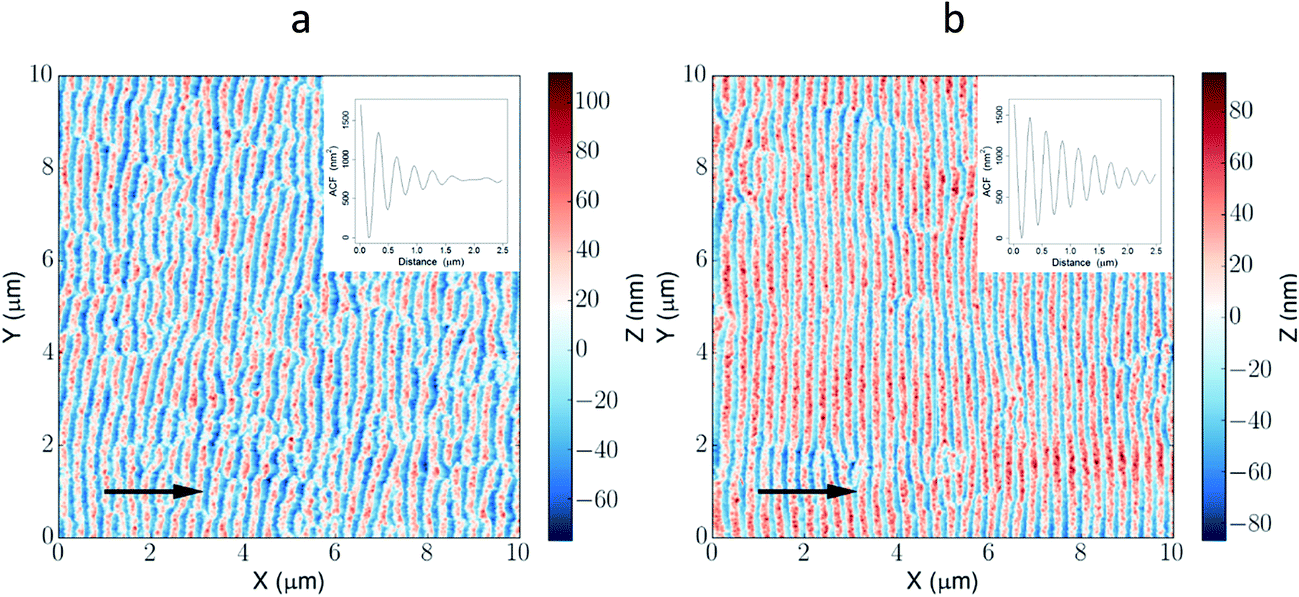 | ||
| Fig. 2 AFM analysis of the irradiated germanium surfaces. AFM topographic images obtained from samples (a) Ge-LD, Au+ fluence of 1 × 10¹⁷ ions per cm2, and (b) Ge-HD, Au+ fluence of 4.3 × 10¹⁷ ions per cm2. The arrows indicate the projection of the ion beam direction. The insets show the 1D height–height ACFs, which were calculated along the x direction, parallel to the ripple wave vector. To get a clearer overall view, in each curve the absolute minimum was set equal to zero. For a better readability of the ACF curves, the inset of (a) is also provided in ESI† as Fig. S3; the inset of (b) is also shown in Fig. 3d. | ||
The AFM study of the transfer process is shown in Fig. 3, while Fig. 4 reports the corresponding SEM study. For Ge-HD, the fundamental ripple spacing (wavelength λ), given by the first peak position of the ACF (Fig. 3d) is λ = 291 nm 95% c.i. [289, 292]. Fig. 3g shows the histogram of the Z heights of the AFM topography of Fig. 3a: a well-shaped two-level distribution is readable, that can be mainly ascribed to the Z distribution of the valleys and to that of the crests of the rippled surface. To estimate the ripple amplitude, described as the mean peak-to-valley excursion, the mean roughness depth RZ was calculated. For sample Ge-HD, the result is RZ = 87 nm ± 13 nm. The 3D topography in Fig. 3j illustrates the high degree of order obtained on the germanium surface in the direction orthogonal to the ion beam. Another pattern of larger quasi-periodicity, oriented parallel to the ion beam, is also visible. This double periodicity is not new,3 and indicates that at the current ion fluence the surface evolution is that characteristic of a non-linear regime.6 The long range correlation of the rippled pattern is confirmed by the SEM image taken at the lowest magnification (Fig. 4a). A higher magnification image of the patterns is reported in Fig. 4b, which shows the presence of the multiscale structure: the ripples show a nanowired structure along the ridges, which is more densely packed on the side opposite the one exposed to the ion beam; in the trenches, stripe-like traces are visible, which are parallel to the direction of the incident beam. The same multiscale structure was also visible for the Ge-LD sample (ESI,† Fig. S4). These structures look similar to the sponge-like morphology which develops on Ge surfaces when irradiated with normally incident heavy ions.11 However, in this study the oblique incident angle does not produce the characteristic isotropically-distributed nanovoids but only a distribution of nano-wires on the ripple crests. It is worth noting that the rounded nature of the amplitude modulation shown by the AFM analysis is actually induced by the finite size of the AFM tip, and the resulting shape also depends on the dynamics of the measurement. In addition to the nanowired structure, the SEM image in Fig. 4b reveals that the shape of the amplitude modulation is better described by a sequence of ridges-and-grooves of comparable width. For the sake of clearness, the periodic patterns will still be called ‘‘ripples” in the remaining of the paper. Nanoporous ripples recalling the structures here discussed were shown but not highlighted in,39 where they had been obtained by irradiating a germanium surface with a 1 × 1017 cm−2 fluence of 30 keV Bi+ ions at 60° of incidence.
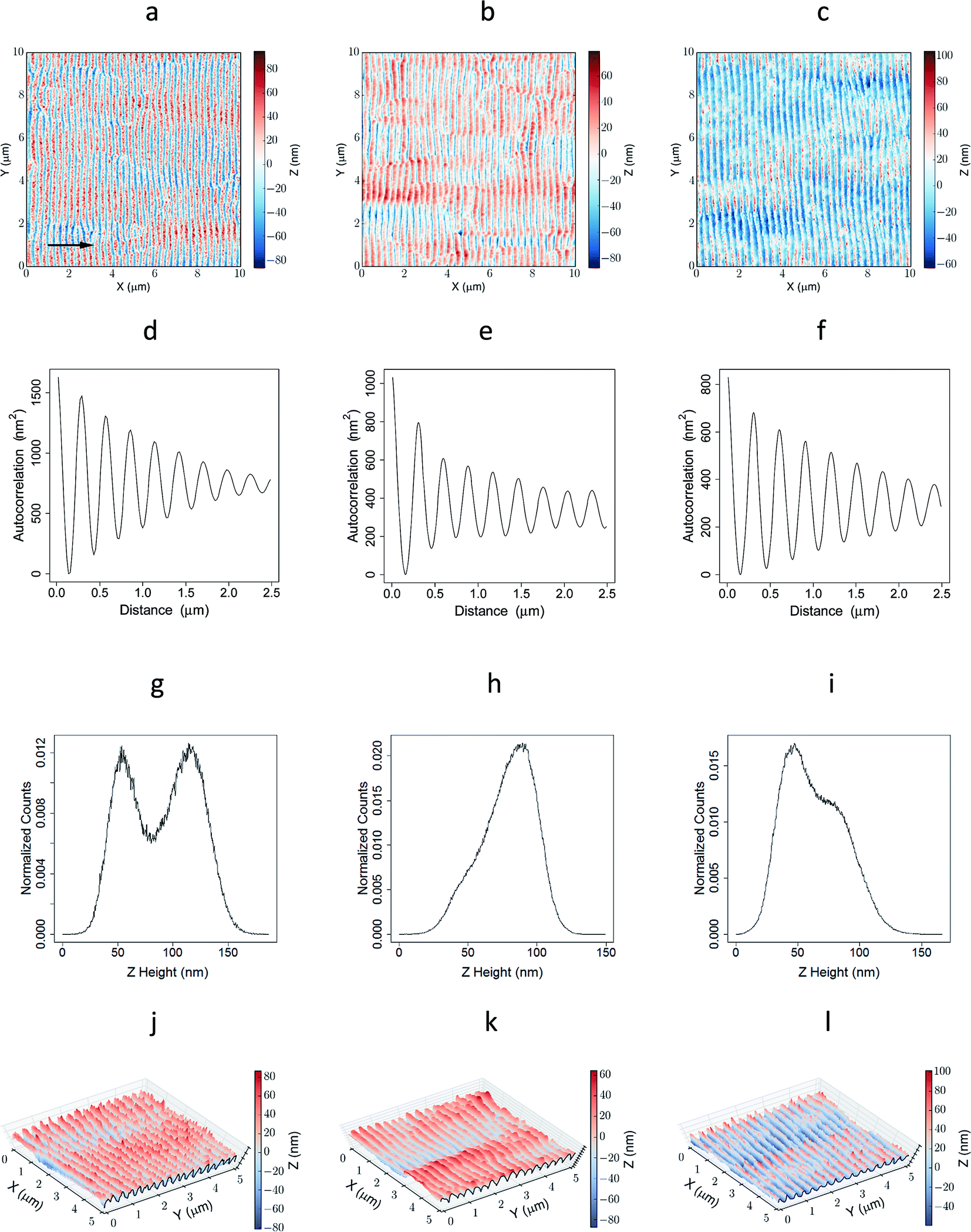 | ||
| Fig. 3 AFM study of the transfer process. AFM 2D topographic images obtained from samples (a) Ge-HD, where the arrow indicates the projection of the ion beam direction; (b) PFPE-HD and (c) COC-HD; (d–f) 1D height–height ACFs, calculated respectively from (a–c) along the direction parallel to the ripple wave vector. To get a clearer overall view, in each curve the absolute minimum was set equal to zero; (g–i) histograms of the surface heights of the AFM topographies in (a–c); (j–l) AFM 3D topography images respectively of sample HD, PFPE-HD and COC-HD, corresponding to one 5 × 5 μm2 portion of the sample areas shown in (a–c). | ||
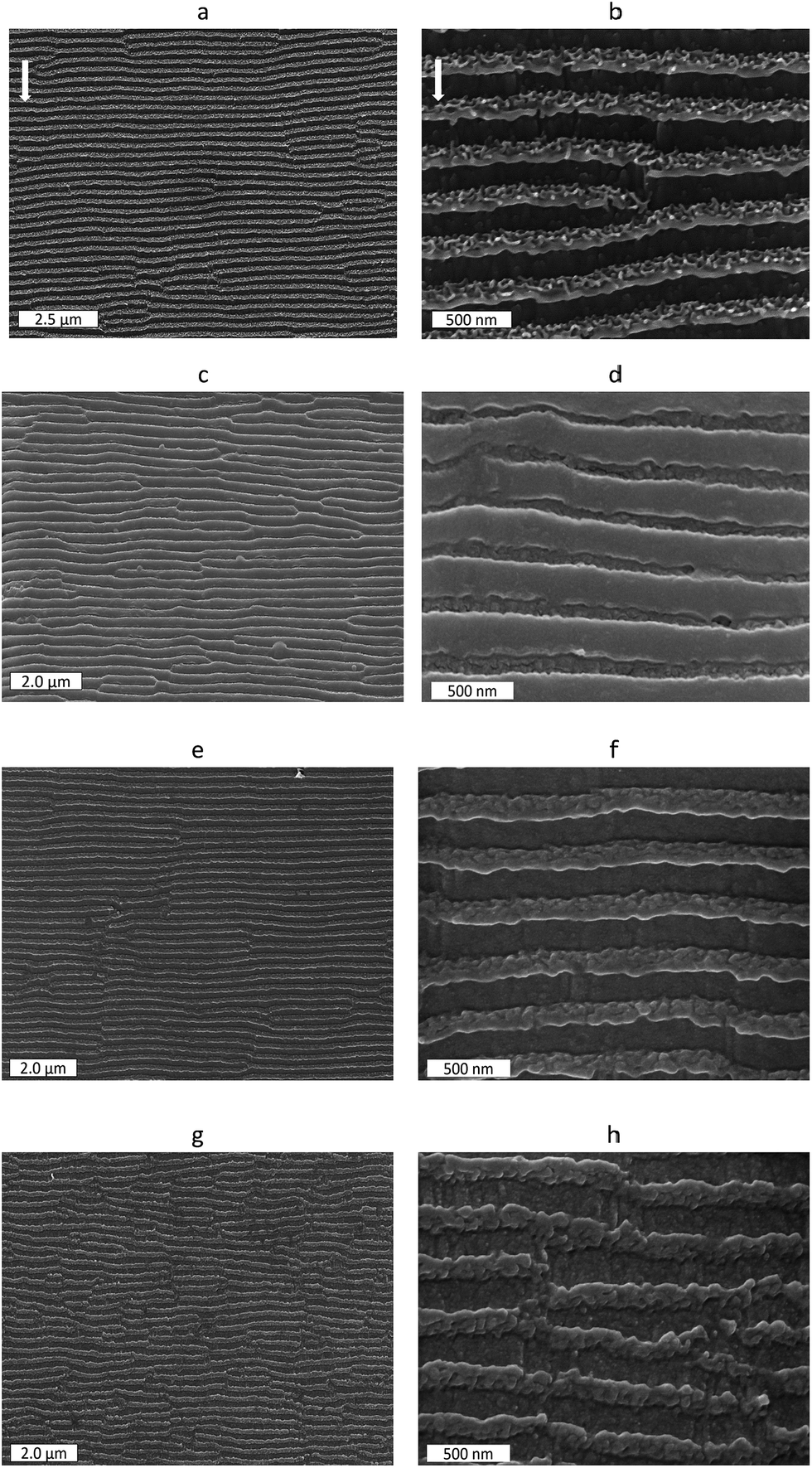 | ||
| Fig. 4 SEM study of the transfer process. SEM images acquired respectively at 10k and 50k magnification from samples (a and b) Ge-HD, where the arrows indicate the projection of the ion beam direction; (c and d) PFPE-HD; (e and f) COC-HD; (g and h) COC-LD. | ||
3.2 The two-step pattern transfer: characterization of the PFPE and COC sample surface
In the thermal NIL described in,28 the transfer of the sub-micron patterns from the original rigid silicon mold to the thermoplastic material required the application of a pressure (typically 50 bar) and heat (up to 150 °C), and the subsequent mechanical detachment of the replica. As a consequence, fractures frequently damaged the original precious mold, which had been obtained by electron-beam lithography and reactive ion etching. PFPE is a soft material, which can be cross-linked by a low-cost UV-curing process, after mixing with an UV initiator (see Section 2.2 for details). Con et al.40 discussed that PFPE has a particularly low surface energy that allows the mold release without the use of agents that accelerate its degradation. They proved that the elastic modulus of the PFPE film is higher on the surface than deep inside the film; hence, the stiff PFPE top surface offers a high resolution in the pattern transfer, whereas the more flexible bulk promotes the conformal contact and an easy demolding. For all these properties, in this study, the intermediate PFPE template allowed the preservation of the fragile and expensive germanium samples and the final transfer of the original rippled nanopatterns onto several COC replicas.The AFM topographic 2D and 3D images of the PFPE mold produced from the Ge-HD sample, here called PFPE-HD, are shown in Fig. 3b and k. The 1D Z–Z ACF in Fig. 3e proves the preservation of the long-range correlation by the transfer process. If compared with Fig. 3j, the 3D image of Fig. 3k is less structured. Since this is the image of the negative surface replica of the germanium sample, the topographic elevations correspond to the original valleys, which are in fact less structured than the crests (see Fig. 4b). Besides, when compared with Fig. 4a and b, the SEM images in Fig. 4c and d show the broadening of the original valleys at the expense of the original crest width. This feature is confirmed by the shape of the histogram of the Z heights shown in Fig. 3h, where the contribution from the original crests, which are partially “buried” in the replica (Fig. 4c and d), only produces a shoulder around 47 nm; the impossibility for the AFM tip to entirely follow the PFPE-HD ripple profile down to the bottom of the amplitude excursion could have further enhanced this histogram characteristic. The cross section TEM analysis in Fig. S1† reveals that the nanowired structures partially shadow the bottom of the valleys; therefore, the negative replica of this structure could produce the cited broadening. This is not only visible in the PFPE-HD sample, but also in the SEM image of the PFPE-LD sample, which is shown in ESI,† Fig. S5.
By a thermal NIL process, the ion beam induced patterns were finally transferred onto COC foils. COC is a thermoplastic material with well-known biocompatibility and optical properties for high-resolution fluorescence microscopy.28 To evaluate the achieved fidelity of the transferred final patterns, the surface morphology and related topographic measurements of the COC final replica of the original Ge-HD, named COC-HD, are reported in Fig. 3c, f, i and l. The long range regularity is preserved, with a wavelength of λ = 304.7 nm 95% c.i. [304.4, 305.0] nm. The calculated mean roughness depth is RZ = 66 nm ± 16 nm, that indicates an overall weak lowering of the structure, if compared with the RZ value of Ge-HD. By inspecting the SEM image of Fig. 4f, a reduced contribution from the nanowired structure on the top of the crests is visible, that can justify the reduced RZ value. This is qualitatively confirmed by Fig. 3i, where the intensity of the peak that represents the contribution of the original crests is reduced with respect to that in Fig. 3g. The mean roughness depth calculated from the 2D AFM topography (ESI,† Fig. S6) of the COC-LD sample is RZ = 98 nm ± 20 nm, which better overlaps the Ge-LD range: RZ = 89 nm ± 15 nm; accordingly, for sample COC-LD the SEM image in Fig. 4h shows a better preserved porous structure. To explain the different residual of the original nanowired structure in sample COC-HD and COC-LD (Fig. 4f and h), the SEM analysis of samples Ge-HD and Ge-LD should be compared (Fig. 4b and S4). An effect of decreasing the ion fluence is, on average, the slight increase of the valley width. Consistently, for Ge-LD the fundamental ripple spacing is λ = 331 nm 95% c.i. [330, 333] nm, which is higher than the value λ = 291 nm 95% c.i. [289, 293] nm, measured for Ge-HD. As a consequence, in the intermediate transfer process a better PFPE conformal contact could be possible for Ge-LD through a more effective infiltration of the PFPE mixture. This is not directly reflected by the AFM measurements on the PFPE replicas: as previously discussed, the broadening in the PFPE samples of the original valleys of the germanium probably hinders the tip from reaching the bottom of the PFPE channel. Accordingly, the RZ values obtained from sample PFPE-HD (Fig. 3b) RZ = 64 nm ± 12 nm, and from sample PFPE-LD (ESI,† Fig. S7) RZ = 60 nm ± 13 nm are in fact comparable, whilst in the final COC replicas RZ is again higher than the corresponding RZ value of sample COC-HD. In conclusion, the finer structures are better preserved for the COC-LD sample, even though structures of sizes well below 100 nm are present in both COC-HD and COC-LD samples (Fig. 4f and h). Therefore, for the investigation of cell–material interaction, a higher degree of the multiscale substrate structure is possible, at the cost of introducing, at the ion irradiation step, a higher degree of topographical noise in the sub-micron rippled pattern (Fig. 4e and g). In fact, keeping constant 26 keV ion energy and 60° incidence angle, the long range regularity of the nanoripples increases with the ion fluence. This behavior is shown in Fig. S8 (ESI†), which presents the SEM images at 10k magnification acquired from the four germanium surfaces irradiated with gold ions at fluence values ranging from 2 × 10¹⁶ ions per cm2 to 4.3 × 10¹⁷ ions per cm2.
4. Conclusion
A new two-step process for transferring multiscale nanopatterns from ion beam irradiated semiconductor surfaces to biocompatible thermoplastic substrates has been demonstrated. Different degrees of regularity of the patterns obtained by Au+ beam irradiation are possible by tuning the ion fluence value. The transfer process via a PFPE intermediate mold to a final COC substrate allows the replication of the original multiscale structure with different degrees of fidelity, with features always well below 100 nm. This ensures in both cases the further investigation of cell–material interaction via topographical cues on different nanoscale sizes. Remarkably, the developed transfer process of rippled patterns obtained by ion implantation foresees its applicability in fields others than the biomedical field here discussed.Acknowledgements
Parts of this research were carried out at IBC at the Helmholtz-Zentrum Dresden – Rossendorf e. V., a member of the Helmholtz Association. The authors thank Gloria Ischia of the Department of Industrial Engineering of the University of Trento for the Pt/Pd coating, and Tiziana Pia Del Buono and Onofrio Antonino Cacioppo of Lfoundry srl, Avezzano (AQ), Italy, for TEM analysis.References
- W. L. Chan and E. Chason, J. Appl. Phys., 2007, 101, 121301 CrossRef.
- S. Facsko, T. Dekorsy, C. Koerdt, C. Trappe, H. Kurz, A. Vogt and H. L. Hartnagel, Science, 1999, 285, 1551 CrossRef CAS PubMed.
- A. Keller and S. Facsko, Materials, 2010, 3, 4811 CrossRef CAS , and references therein.
- B. Teshome, S. Facsko and A. Keller, Nanoscale, 2014, 6, 1790 RSC.
- R. M. Bradley and J. M. E. Harper, J. Vac. Sci. Technol., A, 1988, 6, 2390 CAS.
- R. Cuerno and A. L. Barabási, Phys. Rev. Lett., 1995, 74, 4746 CrossRef CAS PubMed.
- G. Carter and V. Vishnyakov, Phys. Rev. B: Condens. Matter Mater. Phys., 1996, 54, 17647 CrossRef CAS.
- M. Castro, R. Cuerno, L. Vázquez and R. Gago, Phys. Rev. Lett., 2005, 94, 016102 CrossRef PubMed.
- O. El-Atwani, S. A. Norris, K. Ludwig, S. Gonderman and J. P. Allain, Sci. Rep., 2015, 16, 18207 CrossRef PubMed.
- E. Iacob, R. Dell'Anna, D. Giubertoni, E. Demenev, M. Secchi, R. Böttger and G. Pepponi, Microelectron. Eng., 2015, 155, 50 CrossRef.
- L. Romano, G. Impellizzeri, M. V. Tomasello, F. Giannazzo, C. Spinella and M. G. Grimaldi, J. Appl. Phys., 2010, 107, 084314 CrossRef , and reference therein.
- L. Ottaviano, A. Verna, V. Grossi, P. Parisse, S. Piperno, M. Passacantando, G. Impellizzeri and F. Priolo, Surf. Sci., 2007, 601, 2623 CrossRef CAS.
- Q. Wei, X. Zhou, B. Joshi, Y. Chen, K.-D. Li, Q. Wei, K. Sun and L. Wang, Adv. Mater., 2009, 21, 2865 CrossRef CAS.
- R. Böttger, K. H. Heinig, L. Bischoff, B. Liedke and S. Facsko, Appl. Phys. A, 2013, 113, 53 CrossRef.
- I. H. Wilson, Y. J. Chen, J. B. Xu, R. A. B. Devine and C. Jeynes, Surf. Interface Anal., 1996, 24, 881 CrossRef CAS.
- D. Cavalcoli, B. Fraboni, G. Impellizzeri, L. Romano, E. Scavetta and M. G. Grimaldi, Microporous Mesoporous Mater., 2014, 196, 175 CrossRef CAS , and references therein.
- H. Föll, J. Carstensen and S. Frey, J. Nanomater., 2006, 2006, 1 CrossRef.
- G. Kaltsas and A. G. Nassiopoulou, Sens. Actuators, A, 1999, 76, 133 CrossRef CAS.
- H. J. Goldsmid, Materials, 2009, 2, 903 CrossRef CAS.
- M. Isaiev, S. Tutashkonko, V. Jean, K. Termentzidis, T. Nychyporuk, D. Andrusenko, O. Marty, R. M. Burbelo, D. Lacroix and V. Lysenko, Appl. Phys. Lett., 2014, 105, 031912 CrossRef.
- S. A. Mollick, D. Ghose, P. D. Shipman and R. M. Bradley, Appl. Phys. Lett., 2014, 104, 043103 CrossRef.
- D. Sun, A. E. Riley, A. J. Cadby, E. K. Richman, S. D. Korlann and S. H. Tolbert, Nature, 2006, 441, 1126 CrossRef CAS PubMed.
- J. H. Lee, et al., Nano Lett., 2008, 8, 3750 CrossRef CAS PubMed.
- M. Ranjan and S. Facsko, Nanotechnology, 2012, 23, 485307 CrossRef PubMed.
- M. Ranjan, M. Bhatnagar and S. Mukherjee, J. Appl. Phys., 2015, 117, 103106 CrossRef.
- B. Fazio, C. D'Andrea, F. Bonaccorso, A. Irrera, G. Calogero, C. Vasi, P. G. Gucciardi, M. Allegrini, A. Toma, D. Chiappe, C. Martella and F. Buatier de Mongeot, ACS Nano, 2011, 5, 5945 CrossRef CAS PubMed.
- P. Fratzl and R. Weinkamer, Prog. Mater. Sci., 2007, 52, 1263 CrossRef CAS.
- I. Tonazzini, S. Meucci, P. Faraci, F. Beltrama and M. Cecchini, Biomaterials, 2013, 34, 6027 CrossRef CAS PubMed.
- E. J. Tocce, V. K. Smirnov, D. S. Kibalov, S. J. Liliensiek, C. J. Murphy and P. F. Nealey, Biomaterials, 2010, 31, 4064 CrossRef CAS PubMed.
- D. Sengupta and S. C. Heilshorn, Tissue Eng., Part B, 2010, 16, 285 CrossRef CAS PubMed.
- I. Tonazzini, A. Cecchini, Y. Elgersma and M. Cecchini, Adv. Healthcare Mater., 2014, 3, 581 CrossRef CAS PubMed.
- V. Lionetti, M. Cecchini and V. C. Ventura, Stem Cells Dev., 2010, 20, 561 CrossRef PubMed.
- I. Tonazzini, E. Jacchetti, S. Meucci, F. Beltram and M. Cecchini, Adv. Healthcare Mater., 2015, 4, 1849 CrossRef CAS PubMed.
- A. Ferrari, M. Cecchini, M. Serresi, P. Faraci, D. Pisignano and F. Beltram, Biomaterials, 2010, 31, 4682 CrossRef CAS PubMed.
- A. Ferrari, M. Cecchini, A. Dhawan, S. Micera, I. Tonazzini, R. Stabile, D. Pisignano and F. Beltram, Nano Lett., 2011, 11, 505 CrossRef CAS PubMed.
- C. Avigo, N. Di Lascio, P. Armanetti, C. Kusmic, L. Cavigli, F. Ratto, S. Meucci, C. Masciullo, M. Cecchini, R. Pini, F. Faita and L. Menichetti, J. Biomed. Opt., 2015, 20, 046008 CrossRef PubMed.
- R Core Team 2016, R: A language and environment for statistical computing. R Foundation for Statistical Computing., http://www.R-project.org, accessed: 15.12.16.
- G. V. Rossum, Python2.7, Python software foundation, http://www.python.org, accessed 15.12.16, 2016 Search PubMed.
- L. Bischoff, W. Pilz and B. Schmidt, Appl. Phys. A, 2011, 104, 1153 CrossRef CAS.
- C. Con, J. Zhang, Z. Jahed, T. Y. Tsui, M. Yavuz and B. Cui, Microelectron. Eng., 2012, 98, 246 CrossRef CAS.
Footnotes |
| † Electronic supplementary information (ESI) available. See DOI: 10.1039/c6ra28531g |
| ‡ These authors equally contributed to this work. |
| This journal is © The Royal Society of Chemistry 2017 |