
 Open Access Article
 This Open Access Article is licensed under a
 Creative Commons Attribution 3.0 Unported Licence
Electric field induced electronic properties modification of ZrS2/HfS2 van der Waals heterostructure
Jimin Shang ac,
Shuai Zhangb,
Xuerui Chenga,
Zhongming Wei*c and
Jingbo Li*c
ac,
Shuai Zhangb,
Xuerui Chenga,
Zhongming Wei*c and
Jingbo Li*c
aSchool of Physics and Electronics Engineering, Zhengzhou University of Light Industry, Zhengzhou 453002, China
bCollege of Physics and Engineering, Henan University of Science and Technology, Luoyang 471023, China
cState Key Laboratory for Superlattices and Microstructures, Institute of Semiconductors, University of Chinese Academy of Sciences, Chinese Academy of Sciences, Beijing 100083, China. E-mail: zmwei@semi.ac.cn; jbli@semi.ac.cn
First published on 6th March 2017
Abstract
By using first-principles calculations, we investigate the electronic properties of a ZrS2/HfS2 heterostructure modulated by an external electric field. An intrinsic type-I band alignment with an indirect band gap is demonstrated, which can be tuned to become type-II by applying an electric field. The spatial distribution of electron–hole pairs with the lowest energy is accordingly separated between different layers of the heterostructure. Moreover, the band gap exhibits linear variation and a semiconductor-to-metal transition can be realized. The underlying mechanism can be attributed to the linear shifts of band edges along with the quasi-Fermi levels splitting of the respective layers, induced by the charge transfer between layers of the heterostructure driven by the external electric field. Our results provide great application potential of the ZrS2/HfS2 heterostructure in optoelectronic devices.
1. Introduction
Two-dimensional (2D) materials have attracted extensive research in nano- and optoelectronic devices due to their distinctive properties,1–5 and tuning their electronic behaviors also has been important to extend their applications. Recently, it has been found that by combining two different monolayers to form a van der Waals (vdW) heterostructure, one can achieve more desirable properties. For instance, new applications of graphene in semiconductor devices could be increased by forming graphene/h-BN heterostructures,6 the MoS2/WS2 heterostructure presents ultrafast charge transfer in comparison with the single layers,7 and MoS2/Si also exhibits huge potential in solar cell applications.8 Furthermore, it is worth noticing that the band structure of bilayer-MoS2 can be effectively controlled by an electric field, and further realize semiconductor-to-metal transitions in both theoretical and experimental studies.9 The tuning of electronic properties of 2D materials is very important for practical applications in nanoelectronic devices. For instance, to be suitable for high-performance devices, the band gaps of silicene and silicon-based chalcogenide films can all be flexibly modulated by applying an electronic field and strain.10,11 This finding indicates that vdW interactions between layers can lead to effective modulation of electronic properties by various techniques, such as applying strain or an electric field. It is simultaneously expected that more significant effects and interesting properties could be obtained on heterostructures constructed from different 2D materials.As recently fabricated 2D transition metal dichalcogenides (TMDs), ZrS2 and HfS2 have exhibited well-balanced carrier mobility and band gaps, and attracted interest in solar cells and field effect transistors (FETs).10–15 One might try to enhance their carriers’ life through electron–hole separation by constructing heterostructures, and further have better performance in practical applications. More importantly, due to the similar geometric structures and lattice parameters of ZrS2 and HfS2, the lattice-matching problem is naturally satisfied, which will be beneficial in experimental fabrications. Furthermore, the electric field modulation effect should also be of concern to realize more exciting electronic properties.
In this paper, we study the electronic properties of a ZrS2/HfS2 heterostructure modulated by an external electric field. The type-I ZrS2/HfS2 with an indirect band gap can be effectively tuned to become type-II and further realize a semiconductor-to-metal transition. Meanwhile, the spatial distributions of the electron–hole pairs are also successfully separated under an appropriately perpendicular electric field. In addition, the band offsets of the ZrS2/HfS2 heterostructure are also analyzed and found to have linear dependencies on the applied electric field. The relative transitions and variations of band offsets are mainly due to the linear shifts of the band edges along with the quasi-Fermi levels splitting of the respective layers, induced by the charge transfer between the ZrS2 and HfS2 layers of the heterostructure driven by the external electric field.
2. Methods
The calculations are performed within the density-functional theory (DFT) using the generalized gradient approximation (GGA) proposed by Perdew, Burke, and Ernzerhof (PBE) for the exchange and correlation energy.16 Numerical calculations are implemented by the Vienna ab initio simulation package (VASP).17,18 Grimme’s DFT-D2 method is employed to consider the vdW interactions between layers of the heterostructure, which is important in determining the geometric and electronic properties.19 A plane-wave basis with kinetic energy cutoff of 500 eV is used. The Brillouin zone is sampled by 12 × 12 × 1 within Monkhorst–Pack method. The convergence energy for electronic iterations is set as 10−6 eV, and the structures are fully relaxed until the maximum Hellmann–Feynman atomic forces are less than 0.01 eV Å−1. The direction of the external electric field is applied perpendicular to the plane of the ZrS2/HfS2 heterostructure, and the external uniform electric field is disposed with adding an artificial dipole sheet (namely dipole correction).20 A vacuum of 15 Å is sufficient to avoid the interaction between periodic images of slabs in the z-direction.3. Results and discussion
Firstly, we identify the geometric characteristic of ZrS2/HfS2 heterostructure. As can be seen in Fig. 1(a), the 1T-ZrS2 (1T-HfS2) monolayer possesses hexagonal symmetry and a sandwich-like structure, and the lattice constants are optimized to be a = b = 3.66 Å and 3.62 Å, respectively. These are all in good agreement with previous calculated and experimental results.21 Since there are two possible stacking ways (AA and AB) to construct the ZrS2/HfS2 heterostructure (Fig. 1(b)), we compare the total energies of these two patterns and find that AA stacking is more stable than AB stacking by ∼40 meV. Therefore, AA stacking should be more preferred under experimental conditions, and we only focus on it in this study. The lattice parameter of the ZrS2/HfS2 heterostructure is set to be 3.64 Å, thus tiny compressive (ZrS2 layer, <1%) or tensile strains (HfS2 layer, >−1%) can be induced. According to our calculations, such small strains can hardly have any effect on the electronic properties of the respective monolayer. After full relaxation, the interlayer distance (from Zr to Hf) is found to be 6.3 Å. Furthermore, we also check the general PBE method. Our calculations from PBE underestimate the binding energy slightly compared to PBE + vdW, which is consistent with previous reports.11 Due to the same lattice symmetry of the monolayers and the ZrS2/HfS2 heterostructure, the Brillouin zone also remains unchanged (see in Fig. 1(c)). | ||
| Fig. 1 (a) Geometric structures of monolayers of ZrS2 and HfS2. (b) Top and side views of AA and AB stacking ZrS2/HfS2 heterostructures. (c) The Brillouin zone with high symmetry points labeled. | ||
In addition, the structural stability is very important for material applications. To further assess the stability of configurations at room temperature, an ab initio molecular dynamics (MD) simulation is carried out. With a time step of 1 fs, for 3000 fs, the variation of the total energy and temperature with time are considerably small, as shown in Fig. 2. Therefore, we can conclude that there are no obvious distortions of the geometries for the ZrS2/HfS2 heterostructure.
 | ||
| Fig. 2 Ab initio molecular dynamics simulation: the variation of the total energy and temperature with time. | ||
In order to investigate the electronic properties modulation of the ZrS2/HfS2 heterostructure, focusing on the band structures of the respective monolayers is beneficial. As can be seen in Fig. 3(a), the band gaps of monolayer HfS2 and ZrS2 are both found to be indirect with values of 0.99 eV and 1.23 eV, respectively, which are in line with previous calculations.15 Furthermore, we also calculate the projected band structure of ZrS2/HfS2 heterostructure to have an indirect band gap (∼1.02 eV) in Fig. 3(a), where the red and blue circles represent the ZrS2 and HfS2 components of the bands, respectively. It can be seen clearly that the band structures of the monolayer are well maintained and separated, and the band bending of ZrS2 and HfS2 in the heterostructure is small, in comparison with the corresponding monolayer. These findings indicate that the vdW interactions existing between the layers of the ZrS2/HfS2 heterostructure are weak. For the different Fermi levels of the isolated monolayer relative to the vacuum level, the electrons could transfer between two layers once they combine together to form a heterostructure. As can be seen from the scheme of electron energies in Fig. 3(b), the relatively higher Fermi level of monolayer HfS2 in comparison with monolayer ZrS2 can lead to the electron flow from the former to the latter monolayer, while the holes transfer in the opposite direction. As a result, after reaching an equilibrium state between the two sides, the electronic states are found to be mostly located in ZrS2 layer in the vicinity of the Fermi level of the ZrS2/HfS2 heterostructure, and the band alignment becomes type-I accordingly. In this situation, the electron–hole pairs with the lowest energy still stay in the same region, like that of the general monolayer, which could easily lead to the recombination of the carriers and cut short their lifetimes, and be unfavorable for the practical applications of heterostructures in optoelectronics.
 | ||
| Fig. 3 (a) Band structures of monolayer ZrS2, monolayer HfS2, and the ZrS2/HfS2 heterostructure with the Fermi levels all set to be zero. The corresponding band alignments are illustrated in (b), the green and orange dashed lines indicate the Fermi and vacuum levels, respectively. | ||
As we mentioned above, an electric field could effectively tune the electronic properties of the heterostructure. Therefore, we investigate the band alignment modulation of the ZrS2/HfS2 heterostructure by applying an external perpendicular electric field (E⊥), which is important in practical applications.9,22–26 The effect of E⊥ varying from −1.0 V Å−1 to 1.0 V Å−1 is studied, with the positive direction being taken as from HfS2 (top) to ZrS2 (bottom). Our calculation results reveal that applying E⊥ can effectively tune the band alignment and further realize type-I to type-II semiconductor transitions in both positive and negative E⊥ directions. Specifically, it can be seen clearly from Fig. 4(a) that the HfS2 layer and the ZrS2 layer completely occupy the valence band maximum (VBM) and the conduction band minimum (CBM) of the heterostructure, respectively, by applying negative E⊥ = −0.5 V Å−1. In sharp contrast, this becomes the opposite under positive E⊥ = 0.5 V Å−1, the states in the vicinity of the Fermi level are determined by the ZrS2 layer (VBM) and HfS2 layer (CBM), respectively (see Fig. 4(b)). As a result, the CBM and VBM of the heterostructure completely localize on two different layers in space, and the band alignment is tuned from a type-I to type-II semiconductor. Simultaneously, the spatial distributions of electron–hole pairs with the lowest energy are successfully separated to locate on two different layers, which can be beneficial to enhance the life of the carriers in the practical performance of ZrS2/HfS2 heterostructure-based solar cells. For the behaviors of band gap and band edges in the varying of E⊥, we will give more discussion in detail below.
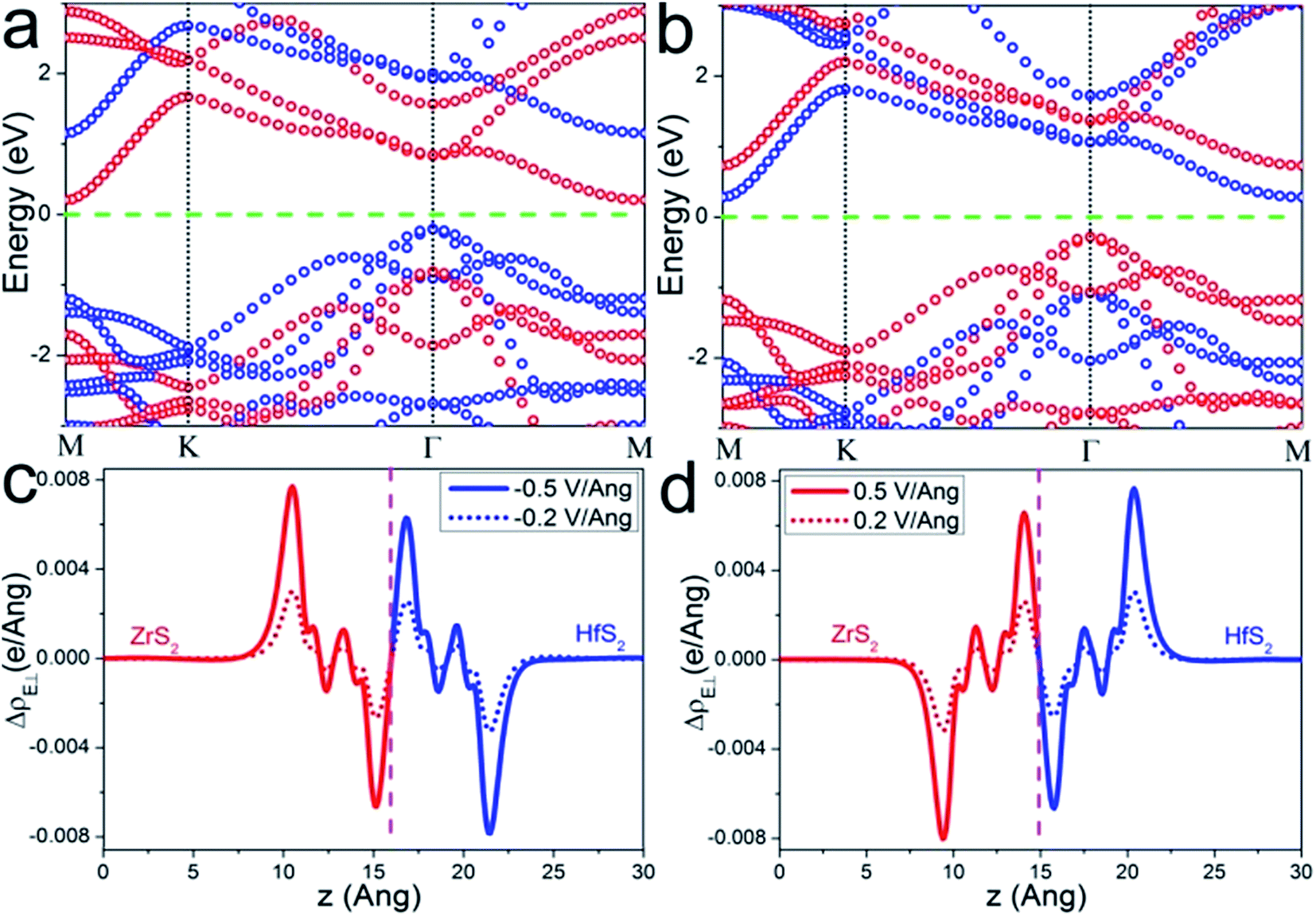 | ||
| Fig. 4 The projected band structure of the ZrS2/HfS2 heterostructure under (a) E⊥ = −0.5 V Å−1 and (b) E⊥ = 0.5 V Å−1. (c and d) The integrated charge density differences of the ZrS2/HfS2 heterostructure under different E⊥, where the blue (red) region corresponds to the HfS2 (ZrS2). | ||
In general, while applying E⊥ on the heterostructure, the electrons (holes) move along the negative (positive) direction of the E⊥ to attain equilibrium. Taking E⊥ with positive values as an illustration, the electrons should transfer from ZrS2 to HfS2 layer, and the holes have the opposite behavior. Accordingly, the quasi-Fermi level of ZrS2 layer (Ef-ZrS2) declines and Ef-HfS2 increases, and then the band edges of ZrS2 and HfS2 layers also could be affected. Both of them are supposed to have same tendencies with their respective quasi-Fermi levels, due to the weak coupling effect between the two layers. When negative E⊥ is applied, the situation is reversed. This could be the main reason why a type-I to type-II semiconductor transition occurs when the applied E⊥ exceeds a certain positive or negative values.
To make it more clear, we calculate the integrated charge density difference under the respective values of E⊥, which is a function of charge density at different position along the perpendicular direction as follows:
 | (1) |
Accordingly, the band gap and band offsets of the heterostructure, which also play important roles in determining the performance of the related devices, could also be tuned. As shown in Fig. 5(a), the band gap variation of the ZrS2/HfS2 heterostructure as a function of E⊥ is described. It can be seen clearly that the band gap is significantly tuned according to a linear relation with E⊥, expect for the regions near E⊥ = 0. When the absolute value of the applied E⊥ is in the range of 0.2–0.7 V Å−1, the band gap decreases linearly with increasing E⊥. Moreover, when E⊥ > 0.7 V Å−1 (<−0.7 V Å−1), the band gap seems close to zero, and a semiconductor-to-metal transition occurs. It is exactly the band offsets and quasi-Fermi levels that determine the band gap and further the band alignments of the ZrS2/HfS2 heterostructure. The valence (conduction) band offset ΔEV (ΔEC) is defined as the difference between the values of valence (conduction) band edges of the two respective layers of the heterostructure. As shown in Fig. 5(a), ΔEV and ΔEC demonstrate similar tendencies, both reduce linearly with increasing E⊥. This can be attributed to the valence and conduction sub-bands of the ZrS2/HfS2 heterostructure undergo splitting under the external electric field, namely the giant Stark effect (GSE), which is analogous to the phenomenon of the Stark effect at atomic level.
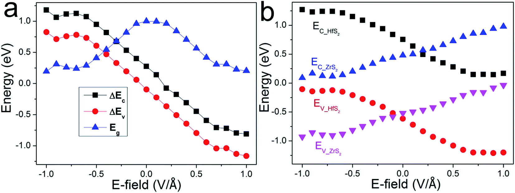 | ||
| Fig. 5 (a) The band gap and band offsets variations of the ZrS2/HfS2 heterostructure as a function of E⊥. (b) The band edges variations of the respective ZrS2 and HfS2 layers in the heterostructure as a function of E⊥. | ||
Further investigation of the variation of the band edges under different E⊥ is presented in Fig. 5(b). The band edges EC-HfS2 (EC-ZrS2) and EV-HfS2 (EV-ZrS2) represent quasi-CBM and quasi-VBM of the HfS2 (ZrS2) layer of the heterostructure, respectively. Similar to the band gap variation tendency, it is distinct that the EC-HfS2 and EV-HfS2 demonstrate approximately linear decreases with increasing E⊥, while the EV-HfS2 and EV-ZrS2 exhibit contrary behaviors. These also demonstrate a weak coupling effect between the layers, and can be mainly attributed to the charge transfer induced by E⊥, which simultaneously leads to the linear shifts of the respective band edges. As we mentioned above, when the applied E⊥ reaches critical values, the band alignment of the heterostructure is tuned from type-I to type-II. It should be noted that the threshold value is different according to the direction of E⊥, about −0.05 V Å−1 and +0.1 V Å−1 respectively. This is mainly due to the band offsets of ZrS2/HfS2 heterostructure having different values without applying an external electric field.
4. Conclusions
To summarize, the electronic properties of the ZrS2/HfS2 heterostructure modulated by external electric field are investigated by using first-principles calculations. Our results reveal that the ZrS2/HfS2 heterostructure demonstrates semiconducting characteristics with an indirect band gap, and the band structures of HfS2 and ZrS2 layers are well preserved with little band bending. More importantly, the band alignment of the ZrS2/HfS2 heterostructure can be effectively tuned from intrinsic type-I to type-II when the applied E⊥ reaches certain values (−0.05 and 0.1 V Å−1). The band gap and band offsets exhibit approximately linear variations with E⊥ expect for the regions nearby E⊥ = 0 and where the gap is being closed. The underlying mechanism can be attributed to the band edges splitting, namely GSE, and the linear band edges shifting, induced by electron transfer between the ZrS2 and HfS2 layers of the heterostructure under the external electric field. Simultaneously, the spatial distribution of electron–hole pairs with the lowest energy is separated, along with the band alignment transforming to type-II. These findings are beneficial to expand potential applications of the ZrS2/HfS2 heterostructure-based field-effect transistors and optoelectronic devices.Acknowledgements
We gratefully acknowledge that this research is supported by projects funded by the National Natural Science Foundation of China (grant no. 11404292 and 11604082) and the Science Foundation of Educational Commission of Henan Province (grant no. 15A140043 and 17B140005).References
- S. Kim, A. Konar and W. S. Hwang, Nat. Commun., 2012, 3, 1011 CrossRef PubMed.
- Y. Li, S. X. Yang and J. B. Li, J. Appl. Phys., 2013, 114, 174307 CrossRef.
- B. Radisavljevic, A. Radenovic and J. Brivio, Nat. Nanotechnol., 2011, 6, 147 CrossRef CAS PubMed.
- C. X. Xia and J. B. Li, J. Semicond., 2016, 37, 051001 CrossRef.
- Q. H. Wang, K. Kalantar-Zadeh and A. Kis, et al., Nat. Nanotechnol., 2012, 7, 699 CrossRef CAS PubMed.
- C. R. Dean and A. F. Young, et al., Nat. Nanotechnol., 2010, 5, 722 CrossRef CAS PubMed.
- X. P. Hong, J. Kim and S. F. Shi, et al., Nat. Nanotechnol., 2014, 9, 682 CrossRef CAS PubMed.
- M. L. Tsai, S. H. Su and J. K. Chang, et al., ACS Nano, 2014, 8, 8317 CrossRef CAS PubMed.
- Q. Liu and L. Li, et al., J. Phys. Chem. C, 2012, 116, 21556 CAS.
- W. Zhang and C. W. Zhang, et al., Appl. Phys. Lett., 2016, 109, 182109 CrossRef.
- W. Zhang and C. W. Zhang, et al., J. Phys. Chem. C, 2014, 118, 25278 Search PubMed.
- W. Zhang and Z. Huang, et al., Nano Res., 2014, 7, 1731 CrossRef CAS.
- L. Li and X. S. Fang, et al., Adv. Mater., 2010, 22, 4151 CrossRef CAS PubMed.
- L. Li, H. Q. Wang and X. S. Fang, et al., Energy Environ. Sci., 2011, 4, 2586 CAS.
- H. Jiang, J. Chem. Phys., 2011, 134, 204705 CrossRef PubMed.
- F. Ortmann, F. Bechstedt and W. G. Schmidt, Phys. Rev. B, 2006, 73, 205101 CrossRef.
- G. Kresse and D. Joubert, Phys. Rev. B, 1999, 59, 1758 CrossRef CAS.
- G. Kresse and J. Furthmuller, Comput. Mater. Sci., 1996, 6, 15 CrossRef CAS.
- S. Grimme, J. Comput. Chem., 2006, 27, 1787 CrossRef CAS PubMed.
- J. Neugebauer and M. Scheffler, Phys. Rev. B: Condens. Matter Mater. Phys., 1992, 46, 16067 CrossRef CAS.
- F. A. Rasmussen and K. S. Thygesen, J. Phys. Chem. C, 2015, 119, 13169 CAS.
- E. K. Yu, D. A. Stewart and S. Tiwari, Phys. Rev. B, 2008, 77, 195406 CrossRef.
- M. Cann, Phys. Rev. B, 2006, 74, 161403 CrossRef.
- T. Chu, H. llatikhameneh and G. Klimeck, et al., Nano Lett., 2015, 15, 8000 CrossRef CAS PubMed.
- L. Huang and N. J. Huo, et al., J. Phys. Chem. Lett., 2015, 6, 2483 CrossRef CAS PubMed.
- L. Huang and J. B. Li, Appl. Phys. Lett., 2016, 108, 083101 CrossRef.
| This journal is © The Royal Society of Chemistry 2017 |