 Open Access Article
Creative Commons Attribution 3.0 Unported Licence
Vertical Al2Se3/MoSe2 heterojunction on sapphire synthesized using ion beam†
Hsu-Sheng Tsai *a,
Jhe-Wei Lioub,
Yi-Chung Wangc,
Chia-Wei Chenc,
Yu-Lun Chuehc,
Ching-Hung Hsiaoc,
Hao Ouyangc,
Wei-Yen Woon*b and
Jenq-Horng Liang*ad
aInstitute of Nuclear Engineering and Science, National Tsing Hua University, Hsinchu 30013, Taiwan, Republic of China. E-mail: b91520016@yahoo.com.tw; jhliang@ess.nthu.edu.tw
bDepartment of Physics, National Central University, Jungli 32054, Taiwan, Republic of China. E-mail: wywoon@phy.ncu.edu.tw
cDepartment of Material Science and Engineering, National Tsing Hua University, Hsinchu 30013, Taiwan, Republic of China
dDepartment of Engineering and System Science, National Tsing Hua University, Hsinchu 30013, Taiwan, Republic of China
First published on 6th February 2017
Abstract
The vertical Al2Se3/MoSe2 heterojunction on sapphire was first fabricated via an ion beam-assisted process. The MoSe2 was formed via Mo selenization, while Al2Se3 was formed via Se substitution for O in sapphire. The applications of this heterojunction will be developed in the future.
Introduction
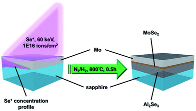
Transition metal dichalcogenides (TMDs)1–4 undoubtedly surpass graphene5 in the application of channel and diode materials because they not only possess proper bandgaps transiting from indirect to direct as the monolayer is reached, but also are stacked by the interlayer van der Waals forces ideally being without dangling bonds. Initially, the single-layer MoS2 transistors were fabricated successfully by Radisavljevic et al.6 and the back-gated MoSe2 field-effect transistors (FETs) were demonstrated by Larentis et al.7 Afterwards, Georgiou et al.8 announced a WS2-based FET on a SiO2/Si substrate and Baugher et al.9 accomplished the in-plane p–n diode of ambipolar WSe2 by electrostatic gating. However, all of the studies mentioned above utilized mechanically exfoliated TMDs for device fabrication, implying that the thickness of TMDs cannot be controlled precisely and the area is limited. The chemical vapor deposition (CVD) method10–12 was also developed for the growth of TMDs on SiO2/Si substrates. Unfortunately, optical microscopy (OM) and/or atomic force microscopy (AFM) images of TMD triangular flakes obtained by CVD growth indicate that the TMD films are non-continuous, even though the dimensions are larger than 100 μm. The non-continuous film completely limits real applications in the semiconductor industry. On the other hand, S or Se corrosion would cause the SiO2 to lose the insulating capability; hence the transfer step seriously deteriorating the quality of TMD films is still inevitable. Another synthesis method13 based on the sulfurization or selenization of transition metal or transition metal oxide films can achieve wafer-scale continuous TMD films. Essentially, the quality of TMD films synthesized by this method is controversial because the crystallinity of e-beam evaporated metal or metal oxide thin films may not be good enough and they could not be uniformly sulfurized or selenized owing to the diffusion-limited reaction. As a result, these might be the main causes leading to the TMD FETs with a carrier mobility as low as 10 cm2 V−1 s−1.13 Zhang et al.14 grew MoSe2 epitaxially on graphene/SiC template to observe the bandgap transition. In fact, the mass production of graphene/SiC template fabricated by the process15 is restricted because it employs an Omicron ultrahigh vacuum (UHV) scanning tunneling microscope (STM) combined with molecular beam epitaxy (MBE) system.For device applications, heterojunctions are the basic units in the electronic device structure; hence the doping method becomes a crucial topic. In addition to electrical control of ambipolar WSe2,9 chemical adsorption16,17 or substitution18,19 doping is the most common technique. Although the cost of chemical doping is relatively low, the adsorbed dopants are much easier to desorb due to the poor stability. The substitution doping is proceeded during the chemical vapor transport (CVT) synthesis of TMDs, requiring high temperature (∼1000 °C) and quite a long period (48–500 h).18,19 Moreover, the large scale TMD films cannot be achieved via the CVT synthesis because the source materials should be sealed in a quartz tube under a vacuum state. Recently, the epitaxial growth of monolayer TMD heterojunctions was reported by several groups.20–23 They claimed that the so-called van der Waals epitaxy could overcome the issue of lattice mismatch, resulting in heteroepitaxial films with a limited area because the interaction between the epitaxial film and substrate is the van der Waals force rather than chemical bonding. Regrettably, the lateral scale of TMD films in these reports still cannot be enlarged, implying that the quality and scale of heteroepitaxial materials depend on several factors and not just the lattice mismatch. Herein, we developed an innovative process using a Se ion beam, as shown in Fig. 1 to directly fabricate a uniformly large scale vertical Al2Se3/MoSe2 junction on sapphire for future applications. The MoSe2 is a semiconductor with a ∼1.55 eV bandgap, while the Al2Se3 is a semiconductor with a ∼3.1 eV bandgap.24,25 The materials were explicitly identified and the formation mechanism could be exhaustively interpreted.
Experimental
Synthesis
A 2-inch sapphire (Al2O3) (0001) wafer was used as the template, in which the Al element was the source of the formation of Al2Se3. A ∼20 nm-Mo thin film was first deposited on the sapphire wafer by customized direct current (DC) sputtering at 25 mTorr. During deposition, the Ar gas with a flow rate of 10 sccm was infused to produce plasma for sputtering. The working voltage and current of the DC power were 277 V and 0.357 A, respectively. The deposition time was 40 s and the substrate was kept at room temperature. The Se ions (60 keV, 1016 ions per cm2) formed from the Se pellets were introduced into the Mo/sapphire wafer by the medium current ion implanter (ULVAC, IMX3500). Finally, the cut samples were annealed at 800 °C with a temperature increasing rate of 20 °C min−1 in the N2/H2 (6/1, v/v) ambiance for 30 minutes. After furnace cooling, the samples are ready for characterization. The dose and energy of implantation were estimated by a SRIM (the stopping and range of ions in matter) simulation in advance.Characterizations
Raman spectroscopy was implemented using a confocal micro-Raman spectrometer (HORIBA, LabRAM, HR800 UV) to be certain of the formation of MoSe2 layers. The light source of the Raman spectrometer was a He–Ne laser with a 632.8 nm wavelength and a power of 35 mW. The surface composition was analyzed using XPS (Ulvac-PHI, Versaprobe II) to confirm the formation of Al2Se3 and MoSe2. The spherical-aberration corrected TEM (JEOL, JEM-ARM200FTH) with a 0.1 nm resolution of the lattice image and 200 kV accelerated voltage was employed to observe the nanoscale layer structure. The distribution of depth concentration was monitored by EDS attached with TEM.Results and discussion
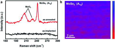
After the conditions of ion implantation were well tuned, the thermal treatment was initially optimized by checking the Raman spectra. The Raman spectrum of the sample obtained by the ion beam-assisted process after optimization was compared with that of the as-implanted sample without annealing. Apparently, there were no Raman peaks that could be observed in the spectrum of the as-implanted sample (Fig. 2a). After the thermal treatment, three Raman peaks located at ∼205, ∼228, and ∼242 cm−1 respectively emerged in the spectrum. The first two peaks were attributed to molybdenum oxide at the surface, resulting from inevitable oxidation during the thermal treatment. The last one was the A1g mode of MoSe2 caused by the out-of-plane vibration.26 The ion implantation technique was chosen for the synthesis of MoSe2 in this study because of its accurate dose and accelerated energy, which could achieve high uniformity and continuity for large-area surface modification. As shown in Fig. 2b, the Raman mapping of the A1g peak of MoSe2 revealed that the MoSe2 film synthesized in this study was uniform and continuous. Thus far, we can confirm that the uniformly continuous MoSe2 film with a large area could be synthesized stably by an ion beam-assisted process. | ||
| Fig. 2 (a) Raman spectra of the as-implanted and as-annealed samples. (b) Raman mapping of the A1g peak of MoSe2. | ||
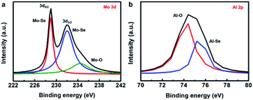
During the experimental design, we considered that the thickness of sputtered Mo film should not be too thin to be uniform. In addition, if the Se ions are implanted into a depth that is not deep enough, they may easily escape from the surface during the thermal treatment because the annealing temperature may be higher than the boiling point of Se. Therefore, we fixed the thickness of the sputtered Mo film to ∼20 nm and set the acceleration energy of implantation at 60 keV, predicting that the maximum concentration of Se would be located at the depth around the Mo/sapphire interface. After Ar+ sputtering through the upper part of Mo film, the X-ray photoelectron spectroscopy (XPS) was implemented to realize the chemical configuration of the interfacial region between the Mo and sapphire. In the Mo 3d spectrum of Fig. 3a, the Mo–Se peak splits into 3d5/2 and 3d3/2 bands, located at ∼229 and ∼232 eV, respectively. This indicates that the Mo near the Mo/sapphire interface has reacted with the Se ions introduced by the implanter. The Mo–O signal (∼234.5 eV) caused by the inevitable oxidation during the thermal treatment was also detected in the Mo 3d spectrum. The signal for Al–O bonding (∼74.4 eV) originates from the sapphire substrate, as shown in Fig. 3b. The Al–Se peak at ∼75.2 eV infers the formation of an Al–Se compound, which might be Al2Se3. XPS indicates that the Se ions near the Mo/sapphire interface might react with the Mo film and Al in the substrate to form MoSe2 and Al2Se3, respectively, during the thermal treatment.
 | ||
| Fig. 3 (a) Mo 3d XPS spectrum of the sample obtained by the ion beam-assisted process. (b) Al 2p XPS spectrum of the sample obtained by the ion beam-assisted process. | ||
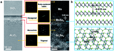
Transmission electron spectroscopy (TEM) was used to monitor the cross-sectional layer structure at nanoscale after the ion beam-assisted process. In the low magnification image of Fig. 4a, the top SiO2 layer deposited by an electron beam evaporator was capped on the surface to protect the thin film from damage during sample preparation using focus ion beam (FIB). In addition, there are two layers with similar thickness (∼20 nm) covering the sapphire substrate. The upper layer should be the Mo film containing MoSe2 layers, while the lower one should be the Al2Se3. Only the lower part of the Mo film could react with the sufficient Se ions to form multilayer MoSe2 with a layer spacing of ∼0.66 nm, which is almost consistent with the theoretical value (∼0.615 nm), as shown in Fig. 4b. In addition, the O atoms in the surface region of sapphire might be substituted with the sufficient Se ions to form an Al2Se3 layer because the maximum concentration of Se is located at the depth around the Mo/sapphire interface. The concentration depth profile was characterized by the energy dispersive spectrometer (EDS). The locations of multilayer MoSe2 and the Al2Se3 layer could be clearly defined, as shown in Fig. S1.† The diffraction patterns of Mo, MoSe2, Al2Se3, and sapphire, shown in the insets in Fig. 4a, were processed by fast Fourier transform (FFT). In addition to MoSe2 with the recognizable layer spacing, Al2Se3 can be identified using its diffraction pattern. The particular interplanar distances of plane groups were computed from two groups of reciprocal lattice points. These two calculated interplanar distances, which are equal to ∼0.4478 and ∼0.241 nm, correspond to the (011) and (400) interplanar distances (Fig. S2†) of Al2Se3, respectively. Furthermore, the angle (∼66°) between the two lines representing the (011) and (400) plane groups in the diffraction pattern is nearly equal to that between the (011) and (400) plane groups in the real lattice (Fig. 4b). Therefore, the layer below MoSe2 could be identified as Al2Se3, as shown in the high magnification image of Fig. 4a. The TEM results, which are in agreement with the EDS line scan results, indicate that the Mo selenization and Se substitution for O in sapphire occur simultaneously during the thermal treatment.
 | ||
| Fig. 4 (a) TEM image of the MoSe2/Al2Se3/sapphire layer structure. Insets: diffraction patterns of Mo, MoSe2, Al2Se3, and sapphire. (b) Atomic models of MoSe2 and Al2Se3. | ||
Conclusion
All the analytical results verify that the lower part of Mo film is selenized and the O atoms of sapphire near the surface are substituted by Se ions introduced by the implanter during the thermal treatment to form a vertical Al2Se3/MoSe2 heterojunction on a sapphire substrate. This is the first study utilizing an ion implantation technique to directly synthesize the vertical heterojunction of TMD/III–VI semiconductor on a sapphire substrate. This simple ion beam-assisted process has great potential for fabricating other types of heterogeneous junctions. In future, we will attempt to develop devices based on this diode for suitable applications.Acknowledgements
Financial support was provided by the Ministry of Science and Technology through Grant No. 104-2221-E-007-104-MY3 and 103-2112-M-008-019-MY3.Notes and references
- I. Song, C. Park and H. C. Choi, RSC Adv., 2015, 5, 7495 RSC.
- M. Bosi, RSC Adv., 2015, 5, 75500 RSC.
- P. V. Sarma, P. D. Patil, P. K. Barman, R. N. Kini and M. M. Shaijumon, RSC Adv., 2016, 6, 376 RSC.
- B. B. Wang, K. Ostrikov, T. van der Laan, K. Zheng, R. Shao, M. K. Zhuf and S. S. Zou, RSC Adv., 2016, 6, 37236 RSC.
- K. S. Novoselov, A. K. Geim, S. V. Morozov, D. Jiang, Y. Zhang, S. V. Dubonos, I. V. Grigorieva and A. A. Firsov, Science, 2004, 306, 666 CrossRef CAS PubMed.
- B. Radisavljevic, A. Radenovic, J. Brivio, V. Giacometti and A. Kis, Nat. Nanotechnol., 2011, 6, 147 CrossRef CAS PubMed.
- S. Larentis, B. Fallahazad and E. Tutuc, Appl. Phys. Lett., 2012, 101, 223104 CrossRef.
- T. Georgiou, R. Jalil, B. D. Belle, L. Britnell, R. V. Gorbachev, S. V. Morozov, Y. J. Kim, A. Gholinia, S. J. Haigh, O. Makarovsky, L. Eaves, L. A. Ponomarenko, A. K. Geim, K. S. Novoselov and A. Mishchenko, Nat. Nanotechnol., 2013, 8, 100 CrossRef CAS PubMed.
- B. W. H. Baugher, H. O. H. Churchill, Y. Yang and P. Jarillo-Herrero, Nat. Nanotechnol., 2014, 9, 262 CrossRef CAS PubMed.
- Y. H. Lee, X. Q. Zhang, W. Zhang, M. T. Chang, C. T. Lin, K. D. Chang, Y. C. Yu, J. T. W. Wang, C. S. Chang, L. J. Li and T. W. Lin, Adv. Mater., 2012, 24, 2320 CrossRef CAS PubMed.
- X. Wang, Y. Gong, G. Shi, W. L. Chow, K. Keyshar, G. Ye, R. Vajtai, J. Lou, Z. Liu, E. Ringe, B. K. Tay and P. M. Ajayan, ACS Nano, 2012, 8, 5125 CrossRef PubMed.
- B. Liu, Y. Ma, A. Zhang, L. Chen, A. N. Abbas, Y. Liu, C. Shen, H. Wan and C. Zhou, ACS Nano, 2016, 10, 5153 CrossRef CAS PubMed.
- P. M. Campbell, A. Tarasov, C. A. Joiner, M. Y. Tsai, G. Pavlidis, S. Graham, W. J. Ready and E. M. Vogel, Nanoscale, 2016, 8, 2268 RSC.
- Y. Zhang, T. R. Chang, B. Zhou, Y. T. Cui, H. Yan, Z. Liu, F. Schmitt, J. Lee, R. Moore, Y. Chen, H. Lin, H. T. Jeng, S. K. Mo, Z. Hussain, A. Bansil and Z. X. Shen, Nat. Nanotechnol., 2014, 9, 111 CrossRef CAS PubMed.
- Q. Wang, W. Zhang, L. Wang, K. He, X. Ma and Q. Xue, J. Phys.: Condens. Matter, 2013, 25, 095002 CrossRef PubMed.
- H. Fang, M. Tosun, G. Seol, T. C. Chang, K. Takei, J. Guo and A. Javey, Nano Lett., 2013, 13, 1991 CrossRef CAS PubMed.
- M. S. Choi, D. Qu, D. Lee, X. Liu, K. Watanabe, T. Taniguchi and W. J. Yoo, ACS Nano, 2014, 8, 9332 CrossRef CAS PubMed.
- J. Suh, T. E. Park, D. Y. Lin, D. Fu, J. Park, H. J. Jung, Y. Chen, C. Ko, C. Jang, Y. Sun, R. Sinclair, J. Chang, S. Tongay and J. Wu, Nano Lett., 2014, 14, 6976 CrossRef CAS PubMed.
- Y. Jin, D. H. Keum, S. J. An, J. Kim, H. S. Lee and Y. H. Lee, Adv. Mater., 2015, 27, 5534 CrossRef CAS PubMed.
- Y. Gong, J. Lin, X. Wang, G. Shi, S. Lei, Z. Lin, X. Zou, G. Ye, R. Vajtai, B. I. Yakobson, H. Terrones, M. Terrones, B. K. Tay, J. Lou, S. T. Pantelides, Z. Liu, W. Zhou and P. M. Ajayan, Nat. Mater., 2014, 13, 1135 CrossRef CAS PubMed.
- C. Huang, S. Wu, A. M. Sanchez, J. J. P. Peters, R. Beanland, J. S. Ross, P. Rivera, W. Yao, D. H. Cobden and X. Xu, Nat. Mater., 2014, 13, 1096 CrossRef CAS PubMed.
- X. Duan, C. Wang, J. C. Shaw, R. Cheng, Y. Chen, H. Li, X. Wu, Y. Tang, Q. Zhang, A. Pan, J. Jiang, R. Yu, Y. Huang and X. Duan, Nat. Nanotechnol., 2014, 9, 1024 CrossRef CAS PubMed.
- M. Y. Li, Y. Shi, C. C. Cheng, L. S. Lu, Y. C. Lin, H. L. Tang, M. L. Tsai, C. W. Chu, K. H. Wei, J. H. He, W. H. Chang, K. Suenaga and L. J. Li, Science, 2015, 349, 524 CrossRef CAS PubMed.
- J. Xia, X. Huang, L. Z. Liu, M. Wang, L. Wang, B. Huang, D. D. Zhu, J. J. Li, C. Z. Gu and X. M. Meng, Nanoscale, 2014, 6, 8949 RSC.
- J. A. Adams, A. Bostwick, T. Ohta, F. S. Ohuchi and M. A. Olmstead, Phys. Rev. B: Condens. Matter Mater. Phys., 2005, 71, 195308 CrossRef.
- P. Tonndorf, R. Schmidt, P. Böttger, X. Zhang, J. Börner, A. Liebig, M. Albrecht, C. Kloc, O. Gordan, D. R. T. Zahn, S. M. de Vasconcellos and R. Bratschitsch, Opt. Express, 2013, 21, 4908 CrossRef CAS PubMed.
Footnote |
| † Electronic supplementary information (ESI) available. See DOI: 10.1039/c6ra28273c |
| This journal is © The Royal Society of Chemistry 2017 |

