
 Open Access Article
 This Open Access Article is licensed under a
 Creative Commons Attribution 3.0 Unported Licence
Synthesis of a monoclinic BiVO4 nanorod array as the photocatalyst for efficient photoelectrochemical water oxidation
Bing-Chang Xiao†
,
Lu-Yin Lin† *,
Jia-Yo Hong,
Hong-Syun Lin and
Yung-Tao Song
*,
Jia-Yo Hong,
Hong-Syun Lin and
Yung-Tao Song
Department of Chemical Engineering and Biotechnology, National Taipei University of Technology (Taipei Tech), Taipei 10608, Taiwan. E-mail: lylin@ntut.edu.tw
First published on 23rd January 2017
Abstract
BiVO4 is one of the most efficient photocatalysts for promoting water oxidation under the framework of Z-scheme water splitting due to its small band gap feature. In this study, the BiVO4 nanorod array was successfully synthesized on fluorine-doped tin oxide (FTO) glasses via a simple solution method, and the electrode was applied as the photoanode for water oxidation. The highest photocurrent density of 0.12 mA cm−2 (measured at 1.23 V vs. RHE) and the smallest onset potential of 0.32 V vs. RHE were obtained for the optimized BiVO4 electrode under AM 1.5G illumination due to the rough surface for promoting light absorption and the one-dimensional (1D) pathway for accelerating the charge transfer, which benefitted from the rod-like structure. Electrochemical impedance spectroscopy was applied to analyze the charge-transfer resistance and electron lifetime of the system. The results suggest that the well-defined nanorod structure can be realized by simply tuning the reaction parameters, and this 1D nanostructure can simultaneously achieve high light absorption and a long electron lifetime, which favor the high photocatalytic ability for water oxidation.
Introduction
Photoelectrochemical (PEC) water splitting over semiconductor photocatalysts has been demonstrated as a promising method to produce clean chemical fuels such as hydrogen to realize solar energy conversion and storage technologies.1–3 O2 production, which involves a four-hole process, is considered to be the rate-determining step for the PEC water splitting system. Hence, the semiconductor for the photocatalytic production of O2 should be carefully designed to enhance the performance of PEC water splitting.4 Developing an applicable semiconductor material is important to meet the requirements for PEC water splitting, such as suitable band-edge potentials, chemical stability, non-toxicity, and low cost.5 Also, the narrow band gap is indispensable for the semiconductor material to achieve efficient visible light absorption since around 46% of the solar spectrum is visible light and only 4% of the solar spectrum is ultraviolet light.6Bismuth vanadate (BiVO4) is one of the most promising photocatalysts for PEC water splitting.7 BiVO4 is able to oxidize water using the holes generated by visible light because of its relatively narrow bandgap of 2.4 eV in the monoclinic phase as well as its particular valence band (formed by Bi 6s or a hybrid orbital of Bi 6s and O 2p) and conduction band (formed by V 3d) structures. Hence, a high theoretical solar to hydrogen (STH) efficiency for BiVO4 is reported to be 9.2% with a photocurrent of 7.5 mA cm−2 under the standard air mass 1.5 global (AM 1.5G) solar light illumination.8 However, the electron transport through the BiVO4 is very poor owing to the high recombination rate of the photogenerated carriers inside the nanomaterial.9 As a result, BiVO4 is characterized by a short carrier diffusion length of only 70 nm,8 which is the main reason for the small photocurrent densities of less than 1 mA cm−2 at 1.23 V reversible hydrogen electrode (RHE) achieved using the BiVO4 photoanodes.10–13 In addition, the slow transfer of the holes at the BiVO4/electrolyte interface also limits the performance of the PEC water splitting using BiVO4 as the photoanode. It has also been reported that the calculated oxidation potential of BiVO4 is slightly more positive (1.24 V versus reversible hydrogen electrode, RHE) than the water oxidation potential (O2/H2O, 1.23 V versus RHE), suggesting that this material could be resistant to photo-induced corrosion under water splitting conditions.14 The calculated oxidation potential may be more negative than the calculated valance edge of the material, as verified by the previous literature.14 Hence, great efforts have been made to improve the photocatalytic properties of BiVO4, e.g., developing heterojunctions,15–17 designing morphologies,18–22 doping ions,23–25 and facet selective deposition.26,27 The morphology design is the most commonly used way to improve the electron transfer of BiVO4 photocatalysts. He et al. reported a simple drop-casting method to synthesize BiVO4 nanoflake array films for photoelectrochemical measurements and obtained a higher photoelectrochemical activity compared to the BiVO4 nanoparticle system. The photocurrent densities of 0.68 and 0.23 mA cm−2 at 1.0 V vs. Ag/AgCl were obtained for the electrodes composed of the BiVO4 nanoflake array and BiVO4, respectively.18 Lu et al. synthesized core–shell structured (CSS) BiVO4 hollow spheres with an ultra-high specific surface area via a one-pot hydrothermal route to achieve superior photocatalytic activity. The photodegradation efficiencies for degrading rhodamine B (RhB) solutions after 4.5 h using the BiVO4 biscuits, plates and CSS hollow spheres were 68%, 88%, and 99%, respectively.19 Li et al. synthesized BiVO4 dendrites using a hydrothermal method without adding an organic surfactant. The enhanced activity in the visible-light photocatalytic degradation of the RhB solution was achieved using this system. After irradiating the visible light for 120 min, the photocatalytic degradation rate was nearly 35%, while 55% of the RhB was removed when the photocatalytic degradation time was 240 min using the BiVO4 dendrites.20 Chen et al. prepared self-assembled BiVO4 samples with red blood cell-like shapes and flower-like microspheres via a solvothermal approach. The prepared BiVO4 samples exhibited excellent photocatalytic activity for the degradation of methyl blue (MB) dye under visible light irradiation.22 Among the literature involving the structural design for the pure BiVO4 photocatalyst, limited works have been made on the synthesis of pure one-dimensional (1D) BiVO4 nanostructures, which have great potential to accelerate the electron transfer via the 1D straight pathways. Instead, the 1D nanostructure using BiVO4 as the photocatalyst for the PEC water splitting was commonly designed by applying the heterojunction structure composed of 1D TiO2 or WO3 nanostructure arrays as the core material coupled with BiVO4 as the light absorber.8,28,29
In this study, a pure 1D BiVO4 nanorod array was successfully made on the fluorine-doped tin oxide (FTO) glass via a simple solution method. The reaction time and temperature were tuned to observe the morphology variation of the BiVO4 nanostructures and the corresponding photoelectrochemical performances for water oxidation. A photocurrent density of 0.12 mA cm−2 measured at 1.23 V vs. RHE and an onset potential of 0.32 V vs. RHE were obtained for the optimized photoanode using the BiVO4 nanorod array as the photocatalyst. The Nyquist plots and the Bode plots were also obtained using electrochemical impedance spectroscopy (EIS) to investigate the charge transfer resistance and the electron lifetime in the electrodes. The results suggest that the structure design for the photocatalyst is of the great importance to achieve effective PEC water splitting.
Experimental
Preparation of BiVO4 electrodes
The fluorine doped tin oxide (FTO) glass (Nippon Sheet Glass, 8–10 Ω □−1, 2.2 mm thick) was cleaned using the neutral cleaner, deionized water, acetone, and acetonitrile sequentially for 15 min under sonication prior to being used as the substrate.The BiVO4 nanostructures were directly grown on the FTO glass as follows. The BiVO4 seed layer was made by spin coating the BiVO4 precursor onto the FTO glass at 4000 rpm for 30 s and then annealing the sample at 400 °C for 5 h in air at the heat and cooling rates of 10 °C min−1. The BiVO4 precursor for the seed layer was prepared as follows. Firstly, 5 mmol of Bi(NO3)3, 5 mmol of NH4VO3, and 10 mmol of citric acid were dissolved into 15 mL of a 23.3% HNO3 aqueous solution, and 0.08 g of polyvinyl alcohol and 0.25 mL of acetic acid were added into 1 mL of the as-prepared solution. Sequentially, the BiVO4 nanostructures were grown on the seed layer by immersing the seed layer-coated FTO glass in the BiVO4 suspension with the FTO side up in an Erlenmeyer flask that was placed in a temperature controlled water bath and connected to a condenser as a reflux system. The BiVO4 suspension was prepared by dissolving 2 mmol of Bi(NO3)3 and 2 mmol of NH4VO3 in 50 mL of a 14% HNO3 aqueous solution and then adding 14.3 g of NaHCO3 in the as-prepared solution under vigorous stirring. The BiVO4 electrodes were prepared using two steps. The first step was to reflux the solution in the flask containing the seed layer-coated FTO glasses at 60 °C with stirring for 4, 5, 6, 8, and 9 h. The second step is similar to the first step but the process was kept at a temperature of 40 °C. Samples prepared in the solution at the same temperatures of 40 and 60 °C for the whole reaction of 12 h were also made for comparison. After the refluxing process, the samples were annealed at 500 °C for 0.5 h in air at the heat and cooling rates of 10 °C min−1.
Material characterization and electrochemical measurements
The morphology of the nanostructures was observed using the field-emission scanning electron microscopy (FE-SEM, Nova NanoSEM 230, FEI, Oregon, USA). The phase and composition of the nanomaterials were examined using the X-ray diffraction (XRD, X'Pert3 Powder, PANalytical) patterns and X-ray photoelectron spectroscopy (XPS, spherical sector analyser, 600 W (Al) 400 W (Mg)). The ultraviolet-visible (UV-vis) spectroscopy was applied to measure the absorption of the electrodes and to estimate the band gap values. The photoelectrochemical measurements were investigated using a potentiostat/galvanostat (PGSTAT 204, Autolab, Eco-Chemie, The Netherlands) with a three-electrode electrochemical system, where the BiVO4 electrodes were used as the working electrode, a Pt wire was used as the counter electrode, and an Ag/AgCl/saturated KCl electrode was used as the reference electrode in an aqueous solution containing 0.5 M Na2SO4 (pH ∼ 7) at a scan rate of 50 mV s−1. All potentials reported were calculated versus the reversible hydrogen electrode (RHE) using eqn (1) as follows.| E (vs. RHE) = E (vs. Ag/AgCl) + 0.05916 × 7 + 0.197 = E (vs. Ag/AgCl) + 0.611 | (1) |
The light source for the simulated sunlight is a 300 Watt xenon lamp equipped with an air mass 1.5G filter (Newport). The EIS was carried out with a three-electrode electrochemical system, where the BiVO4 electrodes were used as the working electrode, a Pt wire was used as the counter electrode, and an Ag/AgCl/saturated KCl electrode was used as the reference electrode in an aqueous solution containing 0.5 M Na2SO4 (pH ∼ 7). The Nyquist plots and the Bode plots were measured in the frequency range from 0.1 to 15![[thin space (1/6-em)]](https://www.rsc.org/images/entities/char_2009.gif) 000 Hz at the potential of 1.23 V vs. RHE under illumination using a potentiostat/galvanostat (PGSTAT 204, Autolab, Eco-Chemie, the Netherlands) equipped with an FRA2 module. The same conditions as those for measuring the Nyquist plots and the Bode plots but at different frequencies of 10, 100, 500, 1000, and 5000 Hz were applied for measuring the Mott–Schottky plots.
000 Hz at the potential of 1.23 V vs. RHE under illumination using a potentiostat/galvanostat (PGSTAT 204, Autolab, Eco-Chemie, the Netherlands) equipped with an FRA2 module. The same conditions as those for measuring the Nyquist plots and the Bode plots but at different frequencies of 10, 100, 500, 1000, and 5000 Hz were applied for measuring the Mott–Schottky plots.
Results and discussion
The effects of the reaction conditions on the physical properties of BiVO4 nanostructures
The structure of the nanomaterials has a large impact on the photoelectrochemical performance of the resulting electrode because of the different surface areas, active sites, and charge transfer paths. Hence, the morphology of the BiVO4 prepared under different conditions was observed using the SEM images, as shown in Fig. 1. Fig. 1(a)–(e) present the BiVO4 nanostructures prepared using the two steps of the refluxing process at 60 °C and 40 °C, respectively, for the first and the second steps. The reaction time for the first and second refluxing processes was the same. Fig. 1(a)–(e) show the BiVO4 nanostructures synthesized using 4, 5, 6, 8, and 9 h for the first and second refluxing processes. Several aggregates connected to form a network on the top layer and were observed for the sample prepared with a 4 h refluxing time in the first and second steps. Additionally, it was found that the aggregates tended to grow in the vertical direction, and smaller nanoparticles were observed on the top of the bigger aggregations when a longer reaction time was applied for the synthesis. Obvious nanorods were obtained with a single nanorod growing separately for the sample prepared with a 6 h reaction time for the two step refluxing processes. Further increasing the reaction time to 8 h, the BiVO4 nanostructure presents larger aggregates on the top layer, and the nanorod morphology was hard to observed, unlike the samples synthesized using a reaction time less than 5 h. The BiVO4 nanostructure prepared using the longest reaction time of 9 h shows fully covered aggregates on the surface, and no rod-like structure can be observed for this case. In addition, to investigate the effects of the reaction temperature and reaction time on the formation of the nanorods, the one step refluxing process was applied to synthesize the BiVO4 nanostructure with a reaction time of 12 h, i.e., the same reaction time to synthesize the nanorod structure (Fig. 1(c)). Fig. 1(f) and (g) present the SEM images for the BiVO4 nanostructures prepared using one step of the refluxing process for 12 h at 40 and 60 °C, respectively. No nanorod structures can be observed for both cases, and the BiVO4 nanostructure synthesized at 40 °C presents a rougher surface than that for the sample prepared at 60 °C, probably because the higher temperature induced the formation of larger aggregations for the latter case. To investigate the morphology variation of the BiVO4 nanostructures synthesized at different refluxing conditions, a schematic illustration is shown in Fig. 2. It was reported that the individual crystal grains can be formed from the decomposition of the amorphous nanoparticles, and during the deposition process, the crystal grains would attach to the seed layer with the VO3− and Bi3+ ions incorporated from the precursor. At higher refluxing temperatures, the VO3− and Bi3+ concentrations would increase and smaller crystal grains can be achieved because of the induced change in the pH values of the solution.30 Hence, the relatively smaller nanoparticle was expected to be synthesized at 60 °C, and the relatively larger nanoparticle was expected to be formed at 40 °C. Based on this assumption, the smaller nanoparticles were expected to be formed in the first step of the refluxing process. The small nanoparticles were expected to form the pyramid base, which would be larger when a longer refluxing time was applied. The second step of the refluxing process proceeded at 40 °C. At this temperature, the larger nanoparticles were expected to grow on the pyramid base formed in the first step of the refluxing process. As illustrated in Fig. 2, the samples prepared using shorter refluxing times for the first and second steps (4 and 5 h) may have smaller pyramid bases and smaller particles deposited on the base, leading to a flat surface with spread particle aggregations. When the longer refluxing times (6 and 8 h) were applied for the synthesis, larger pyramid bases were formed at the first refluxing process, and larger particles would grow on the base at the second refluxing process to form the nanorod structure. However, when the longest refluxing time (9 h) was used to prepare the BiVO4 nanostructure, the big nanoparticles probably piled on the top layer, and the nanorod structure could not be observed. In all, the BiVO4 synthesized using different temperatures would present different sizes of nanoparticles. The reaction time for the processes conducted at 40 and 60 °C also plays an important role in the morphology of the BiVO4 piled by nanoparticles. The nanorod-like structure can only be achieved using 6 h for the two-step reactions at 40 and 60 °C for the first and second reaction, respectively.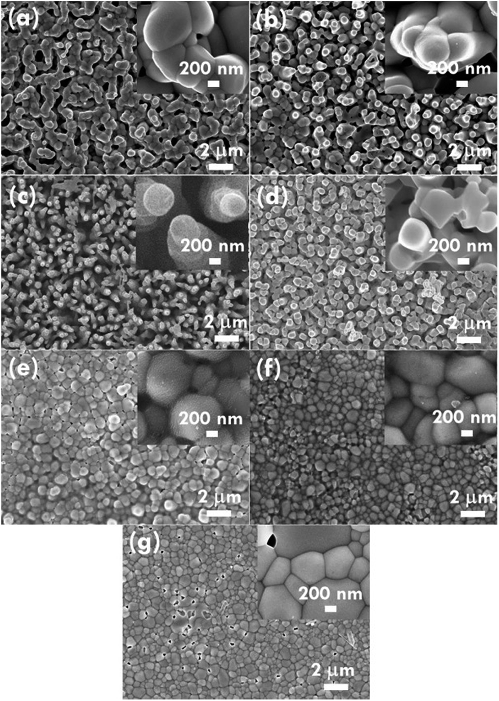 | ||
| Fig. 1 The SEM images for the BiVO4 electrode synthesized using reaction times of (a) 4 h, (b) 5 h, (c) 6 h, (d) 8 h, and (e) 9 h for the first and second step of the refluxing process and 12 h for the one step refluxing process with the reaction temperature of (f) 40 °C and (g) 60 °C. | ||
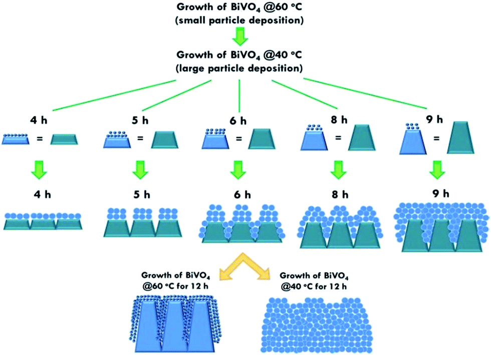 | ||
| Fig. 2 The scheme for illustrating the growth of BiVO4 prepared in different conditions. The cartons in the top side present the growth of the BiVO4 nanostructures in two steps. The reaction temperatures for the first and second steps are 60 and 40 °C, respectively. The cartons in the bottom side present the growth of the BiVO4 nanostructures in the one step with a reaction time of 12 h, and the reaction temperature was kept at 40 or 60 °C for the whole reaction process. | ||
Furthermore, the composition and phase of the samples were analyzed using XRD patterns, as shown in Fig. 3(a). The peaks for the FTO layer were indicated by the star symbol. The monoclinic phase of the BiVO4 (m-BiVO4) (JCPDS no. 01-083-1699) can be observed for the samples prepared using 5 and 6 h for the two step refluxing processes, and the BiVO4 electrode prepared using 6 h for the two step refluxing processes shows relatively strong peaks corresponding to the plane of (112), (004), (015), (116), and (031). In addition, the BiVO4 electrodes prepared using 4, 8, and 9 h for the two step refluxing processes present much weaker signals for the peaks detected at smaller degrees compared to those synthesized using 5 and 6 h for the two step refluxing process. It is inferred that the crystallinity increases when the reaction time increases from 4 to 6 h, probably due to the longer time for the dissolution and recrystallization in the crystal formation process. However, the crystallinity decreases when longer reaction times of 8 and 9 h were applied for the synthesis. The result is likely owing to the dissolution of the crystals at such a long reaction time for the synthesizing process. On the other hand, the clear monoclinic phase of BiVO4 was found for the samples synthesized using the one step refluxing process with a reaction time of 12 h at 40 and 60 °C. It is inferred that for the synthesis conducted at the same temperature in the one step refluxing process, the crystal would be easier to grow since similar size nanoparticles were formed at the same reaction temperature, and the pile of the nanoparticles would be more regular when the sizes of the nanoparticles are very similar. Moreover, for the samples prepared using the one step refluxing process, the sample prepared at 60 °C shows higher intensities, especially for the peaks assigned to the plane of (112) and (220) compared to those of the sample synthesized at 40 °C, owing to the higher kinetic energy of the VO3− and Bi3+ ions induced by using the higher reaction temperature to form the higher crystallinity nanostructure. To further confirm the composition of the sample, Fig. 3(b) presents the energy-dispersive X-ray spectroscopy (EDX) spectrum of the sample prepared using 6 h for the first and second step of the refluxing process. The signals for Bi, V, and O were clearly detected in the spectrum, again confirming the composition of the BiVO4 nanorod array. Furthermore, the XPS spectra of each element of the BiVO4 nanostructures are shown in Fig. 4. The survey XPS spectrum as well as the spectra for the Bi, V, and O are shown in Fig. 4(a)–(d). The binding energies of Bi 4f7/2 (157.9 eV), Bi 4f5/2 (163.2 eV), V 2p3/2 (515.8 eV), and O 1s (529.1 eV) were obtained for all the BiVO4 nanostructures, again suggesting the successful growth of the monoclinic BiVO4 photocatalysts. In all, by using this simple solution method, BiVO4 can be obtained for all of the samples. However, the BiVO4 nanostructures prepared using different reaction temperatures and times will present various crystallinities, which may influence their electrochemical performances.
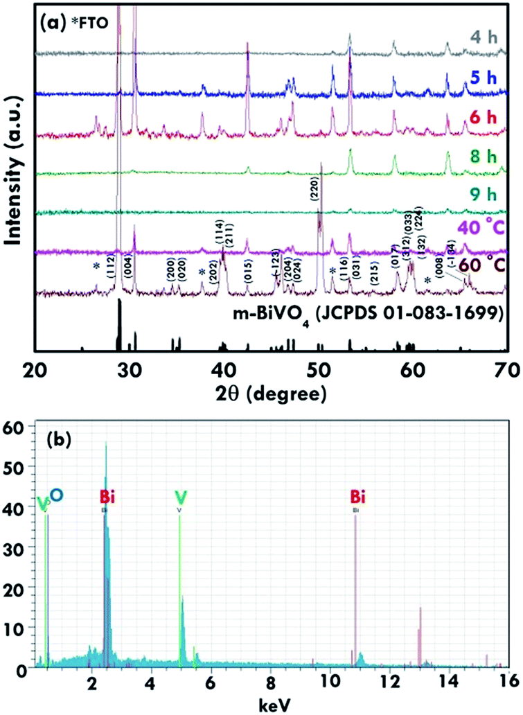 | ||
| Fig. 3 (a) The XRD patterns for the BiVO4 electrodes synthesized using a reaction time of 4 h at 40 °C and 4 h at 60 °C (4 h), 5 h at 40 °C and 5 h at 60 °C (5 h), 6 h at 40 °C and 6 h at 60 °C (6 h), 8 h at 40 °C and 8 h at 60 °C (8 h), 9 h at 40 °C and 9 h at 60 °C (9 h), 12 h at 40 °C (40 °C) and 12 h at 60 °C (60 °C), and (b) the EDX spectrum for the BiVO4 electrode synthesized using a reaction time of 6 h for the first and second step of the refluxing process. | ||
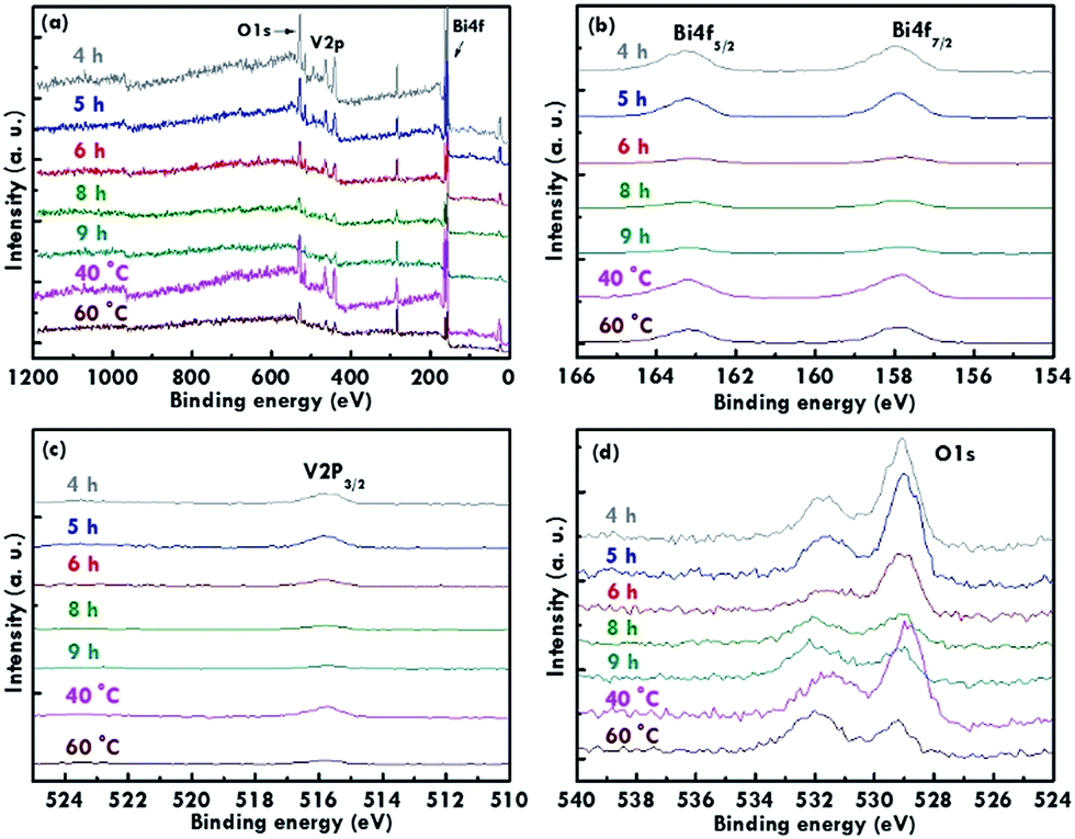 | ||
| Fig. 4 The XPS spectra of the BiVO4 prepared using different reaction times and temperatures. (a) The survey XPS spectrum, (b) Bi 4f, (c) V 2p, and (d) O 1s peaks related to the BiVO4 photocatalyst. | ||
In addition, the light absorption features of the BiVO4 electrodes were measured using UV-visible spectroscopy, as shown in Fig. 5(a). The absorption edge was obtained at a wavelength of around 500 nm for all the electrodes, suggesting the successful synthesis of the monoclinic BiVO4 electrodes.31 The absorption was found to be the highest for the BiVO4 electrode prepared using 6 h as the reaction time for the first and second refluxing process. The absorption decreases for the BiVO4 electrodes synthesized using 8, 5, 4, 9 h for the first and second refluxing process. As observed from the SEM images, individual growth of the rod-like structure was obtained for the BiVO4 electrode synthesized using 6 h for the first and second refluxing process. The sample synthesized using 8 h for the first and second refluxing processes also presents a rod-like structure, but some aggregations were observed between the nanorods. In addition, the morphology of the BiVO4 nanostructure becomes flatter and flatter when reaction times of 5, 4, and 9 h were applied to synthesize the samples in the first and second refluxing processes. The flat surface may have a higher reflection than the rod-like structure, since the rod-like structure has deep gaps in-between the rods to confine the light reflection from the structure. On the other hand, Fig. 5(b) shows the Tauc plot obtained using the absorption spectra (Fig. 5(a)), and the Tauc equation shown in eqn (2) as follows:32
| (αhν)n = A(hν − Eg) | (2) |
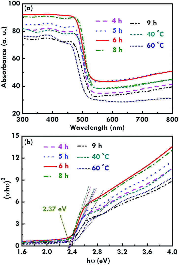 | ||
| Fig. 5 (a) Absorption spectra and (b) Tauc plots for BiVO4 electrodes synthesized using a reaction time of 4 h at 40 °C and 4 h at 60 °C (4 h), 5 h at 40 °C and 5 h at 60 °C (5 h), 6 h at 40 °C and 6 h at 60 °C (6 h), 8 h at 40 °C and 8 h at 60 °C (8 h), 9 h at 40 °C and 9 h at 60 °C (9 h), 12 h at 40 °C (40 °C), and 12 h at 60 °C (60 °C). | ||
The electrochemical performance of the BiVO4 electrodes
Furthermore, the photocurrent density–voltage (J–V) curves were measured using linear sweep voltammetry (LSV) to estimate the electrochemical performance of the BiVO4 electrodes under simulated AM 1.5G illumination at a power density of 100 mW cm−2. The J–V curves for the BiVO4 electrodes prepared using the two step refluxing processes are shown in Fig. 6(a). The onset potentials of 0.42, 0.36, 0.32, 0.38 and 0.44 V vs. RHE were obtained for the BiVO4 electrodes synthesized using 4, 5, 6, 8, and 9 h for the first and second refluxing processes, respectively. The BiVO4 electrodes prepared using 6 h for the two step refluxing process present the smallest onset potential due to the one-dimensional rod-like structure, which reduced the recombination of the charges. The more negative onset potential is advantageous for the Z-scheme system, which requires a low onset potential for the photoanode to integrate with a photocathode.34 On the other hand, photocurrent densities of 0.07, 0.09, 0.12, 0.04, and 0.02 mA cm−2 were obtained at 1.23 V vs. RHE for the BiVO4 electrode synthesized using 4, 5, 6, 8, and 9 h for the first and second refluxing processes, respectively. The highest photocurrent density obtained for the BiVO4 electrode prepared using 6 h for the two step refluxing process can be attributed to the highest absorption of the incident light to excite more electron/hole pairs in the material and the better crystallinity to transfer the charges in the rod-like structure. The morphology gradually deviates from the nanorod structure, and the crystallinity tends to be lower when the reaction time for synthesizing the BiVO4 electrodes becomes shorter or longer than 6 h, leading to a smaller photocurrent density for the corresponding photoanodes.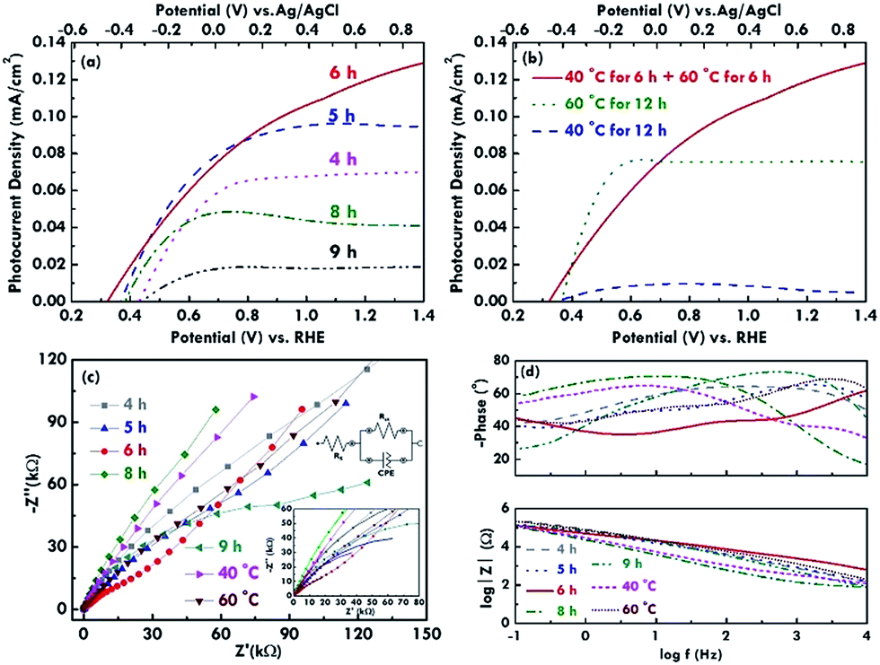 | ||
| Fig. 6 The J–V curves for BiVO4 electrodes synthesized using reaction time of (a) 4 h at 40 °C and following 4 h at 60 °C (4 h), 5 h at 40 °C and following 5 h at 60 °C (5 h), 6 h at 40 °C and following 6 h at 60 °C (6 h), 8 h at 40 °C and following 8 h at 60 °C (8 h), as well as 9 h at 40 °C and following 9 h at 60 °C (9 h) and (b) 6 h at 40 °C and following 6 h at 60 °C (6 h), 12 h at 40 °C (40 °C), and 12 h at 60 °C (60 °C); (c) Nyquist plots with the equivalent circuit inserted and (d) Bode plots measured at 1.23 vs. RHE under visible light irradiation (100 mW cm−2) for the BiVO4 electrodes as the same as those measured in (a) and (b). | ||
On the other hand, the J–V curves for the BiVO4 electrodes prepared using a reaction time of 12 h are shown in Fig. 6(b). The BiVO4 electrode prepared using 6 h for the two step refluxing process presents the highest photocurrent density compared to those synthesized using the one step refluxing process. This is probably because the nanorod structure for the former case enhances the charge transfer via the 1D rod-like structure. Moreover, the BiVO4 electrode synthesized using 60 °C for the two step refluxing process possesses a higher photocurrent density compared to that for the sample prepared using 40 °C for the two step refluxing process. The result is probably because of the higher crystallinity for the sample prepared using the higher reaction temperature of 60 °C. Furthermore, the conductivity and charge-transfer resistance of the BiVO4 electrodes were evaluated using the EIS technique. The Nyquist plots for BiVO4 electrodes prepared under various refluxing conditions are shown in Fig. 6(c). The enlarged plots in the high frequency region along with the fitted curves and the equivalent circuit were also inserted in this figure. The series resistance (Rs) indexed to the conductivity of the electrode can be estimated using the interception in the x-axis, and the charge-transfer resistance (Rct) at the interface between the electrolyte and the BiVO4 nanostructure can be estimated by observing the semicircle at the high frequency region.35,36 The Rs values of around 50 to 70 Ω were obtained for all the samples. The similar Rs values suggest the conductivity varies limitedly when different refluxing conditions were applied to synthesize the BiVO4 nanostructures. On the other hand, the BiVO4 electrode prepared using 6 h for the first and second refluxing processes shows the smallest Rct value of 33.3 kΩ among all the samples. Also, for the samples prepared using 12 h as the reaction time, the BiVO4 electrode synthesized using 6 h for the first and second refluxing processes presents the smallest Rct value, and the sample prepared using 60 °C as the refluxing temperature for the one step refluxing process shows a smaller Rct value than the sample synthesized using 40 °C as the refluxing temperature for the one step refluxing process. It was inferred from these results that the morphology and crystallinity of the BiVO4 nanostructures have a large impact on the charge transfer resistance at the interface of the electrode. The rod-like structure and high crystallinity favor the smaller charge transfer resistance and less recombination of the charges. On the other hand, the Bode plots for the BiVO4 electrodes are shown in Fig. 6(d), and they investigate the electron lifetime in the nanostructure. The peak of the phase angle curves indicates the speed of the charge transfer at the interface of the electrode.12 The peak of the phase angle was found to appear at the highest frequency for the BiVO4 electrode prepared using 6 h as the first and second refluxing processes, suggesting the charge transfer phenomenon is fastest for this case. The result is due to the rod-like structure and is consistent with its lowest onset potential. In all, the best photoelectrochemical performance was obtained for the BiVO4 nanorod electrode prepared using 6 h for the first and second reactions with the highest photocurrent density, the smallest onset potential, and the smallest charge transfer resistance at the electrode and electrolyte interface.
After applying the EIS technique to analyse the electrochemical performances, the transient current response was measured under chopped illumination (measured at 1.23 V vs. RHE) to confirm the solar-driven water splitting and evaluate the recombination phenomenon of the electrode in a short time, as shown in Fig. 7(a). The photocurrent response presents a spike when the light was switched on and then shows a steady state during the illumination period. On the contrary, when the light was switched off, the photocurrent shows an over-shoot, and then the current decays back to zero during the dark period. The phenomenon is because the photo-generated electrons and holes are separated when the light is on. Then, the electrons move towards the current collector and the holes move towards the surface of the semiconductor at the same time under continuous illumination. The concentration of the holes on the surface of the semiconductor increases until a steady-state concentration is reached. The steady-state is maintained with the holes arriving in the surface of the semiconductor and the recombination of the charges. The positive transient may be caused by the surface state trapping. Hence, the slow water oxidation kinetics of the holes at the surface of the photoanode, while the negative transients of the photocurrent may reflect the recombination of photo-generated electrons with accumulated holes. Moreover, the long-term stability of the electrode using the BiVO4 nanorod array as the photocatalyst for the photoelectrochemical water oxidation was evaluated with the electrode held at 1.23 V vs. RHE under simulated AM 1.5G illumination to monitor the photocurrent density, as shown in Fig. 7(b). The normalized photocurrent density for the BiVO4 electrode remained at about a 57% retention compared to the initial value over 1000 min of illumination, suggesting the good stability of the BiVO4 nanorod array as a photocatalyst under continuous illumination.
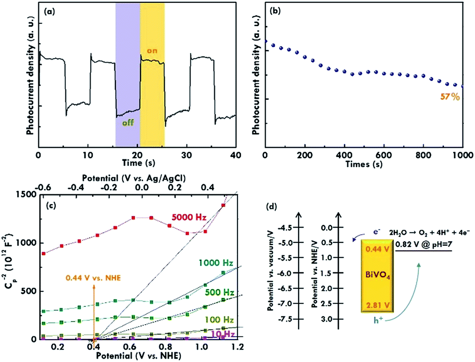 | ||
| Fig. 7 (a) The transient photocurrent plots, (b) the current measurement for the stability test, (c) the Mott–Schottky plots obtained at different frequencies, and (d) the schematic representation of band energies for the optimized BiVO4 electrode. | ||
Last, the band structure of the BiVO4 nanorod was investigated using the Mott–Schottky plots in which the flat band potentials (Efb) were obtained by extrapolating the curves, as shown in Fig. 7(c). The frequencies of 10, 100, 500, 1000, and 5000 Hz were applied for the measurement, and an intercept on the x-axis of around 0.44 V was obtained for all the cases, suggesting an Efb value of 0.44 V (vs. NHE at pH 7) for the BiVO4 electrode. Principally, the Eft value is inferred to be located just under the conduction band of n-type semiconductors.37 The slight difference between the flat band potential (0.44 V) and the onset potential (0.32 V) of BiVO4 may be caused by the rate limitation due to the charge transfer across the semiconductor–electrolyte interface and recombination in the space‐charge layer. The low electron and hole transfer currents across the interface are attributed to the weak overlap between the semiconductor bands and redox ion state densities. Therefore, the conduction band (CB) for BiVO4 is considered to be 0.44 V vs. NHE, as the reference of the Efb obtained in the Mott–Schottky plot. In considering the band gap of 2.37 eV obtained from the Tauc plots and the CB of 0.44 V vs. NHE estimated from the Mott–Schottky plots, a valence band (VB) edge of 2.81 V vs. NHE was obtained for the BiVO4 electrode, as illustrated in the band structure shown in Fig. 7(d). The conduction and valence band edges are reported to be about 4.77 and 7.27 eV below the vacuum level for the BiVO4.14 These values correspond to 0.27 and 2.77 eV vs. RHE. The valance band edge calculated from our work (2.88 eV vs. RHE) is thus close to the value obtained from previous literature (2.77 eV vs. RHE).14 In all, these values for the band positions are similar to those reported in the previous literature, confirming the BiVO4 nature for the nanorod sample prepared using the simple solution method in this work.
Conclusions
The BiVO4 nanorod array was successfully synthesized on a FTO glass using a simple two step refluxing solution method. The refluxing temperature and time were optimized regarding the morphology and crystallinity of the nanostructure as well as the electrochemical performance of the supercapacitor electrode. A higher crystallinity was achieved when a higher reaction temperature was applied for the synthesis. An absorption edge at a wavelength of around 500 nm and an optical band gap of 2.37 eV were obtained for all the electrodes. The smallest onset potential of 0.32 V vs. RHE and the highest photocurrent density of 0.12 mA cm−2 at 1.23 V vs. RHE were obtained for the BiVO4 electrodes synthesized using 6 h as the reaction time for the first and second refluxing processes due to the highest absorption of the incident light to excite more electron/hole pairs as well as better crystallinity and rod-like structure to enhance charge transfer at the interfaces.Acknowledgements
This work was supported in part by the Ministry of Science and Technology of Taiwan, under grant numbers: MOST 103-2218-E-027-010-MY2 and MOST 103-2119-M-027-001.Notes and references
- J. Xing, W. Q. Fang, H. J. Zhao and H. G. Yang, Chem.–Asian J., 2012, 7, 642–657 CrossRef CAS PubMed
.
- S. J. A. Moniz, S. A. Shevlin, D. J. Martin, Z. X. Guo and J. Tang, Energy Environ. Sci., 2015, 8, 731–759 CAS
- Z. F. Huang, L. Pan, J. J. Zou, X. Zhang and L. Wang, Nanoscale, 2014, 6, 14044–14063 RSC
- K. Fuku and K. Sayama, Chem. Commun., 2016, 52, 5406–5409 RSC
- A. Kudo and Y. Miseki, Chem. Soc. Rev., 2009, 38, 253 RSC
- C. Hu, J. Xu, Y. Zhu, A. Chen, Z. Bian and H. Wang, Environ. Sci. Pollut. Res., 2016, 23, 18421–18428 CrossRef CAS PubMed
- T. W. Kim and K.-S. Choi, Science, 2014, 343, 990–994 CrossRef CAS PubMed
- Y. Pihosh, I. Turkevych, K. Mawatari, J. Uemura, Y. Kazoe, S. Kosar, K. Makita, T. Sugaya, T. Matsui, D. Fujita, M. Tosa, M. Kondo and T. Kitamori, Sci. Rep., 2015, 5, 11141 CrossRef PubMed
- S. J. A. Moniz, J. Zhu and J. Tang, Adv. Energy Mater., 2014, 4, 1301590 CrossRef
- L. Zhang, E. Reisner and J. J. Baumberg, Energy Environ. Sci., 2014, 7, 1402 CAS
- V. Nair, C. L. Perkins, Q. Lin and M. Law, Energy Environ. Sci., 2016, 9, 1412–1429 CAS
- S. Hernández, G. Gerardi, K. Bejtka, A. Fina and N. Russo, Appl. Catal., B, 2016, 190, 66–74 CrossRef
- M. Zhou, J. Bao, W. Bi, Y. Zeng, R. Zhu, M. Tao and Y. Xie, ChemSusChem, 2012, 5, 1420–1425 CrossRef CAS PubMed
- F. M. Toma, J. K. Cooper, V. Kunzelmann, M. T. McDowell, J. Yu, D. M. Larson, N. J. Borys, C. Abelyan, J. W. Beeman, K. M. Yu, J. Yang, L. Chen, M. R. Shaner, J. Spurgeon, F. A. Houle, K. A. Persson and I. D. Sharp, Nat. Commun., 2016, 7, 12012 CrossRef PubMed
- H. Jung, S. Y. Chae, C. Shin, B. K. Min, O. S. Joo and Y. J. Hwang, ACS Appl. Mater. Interfaces, 2015, 7, 5788–5796 CAS
- E. S. Kim, H. J. Kang, G. Magesh, J. Y. Kim, J. W. Jang and J. S. Lee, ACS Appl. Mater. Interfaces, 2014, 6, 17762–17769 CAS
- X. Gao, H. B. Wu, L. Zheng, Y. Zhong, Y. Hu and X. W. Lou, Angew. Chem., Int. Ed. Engl., 2014, 53, 5917–5921 CrossRef CAS PubMed
- H. He, S. P. Berglund, A. J. E. Rettie, W. D. Chemelewski, P. Xiao, Y. Zhang and C. B. Mullins, J. Mater. Chem. A, 2014, 2, 9371 CAS
- Y. Lu, Y. S. Luo, H. M. Xiao and S. Y. Fu, CrystEngComm, 2014, 16, 6059 RSC
- D. Li, W. Shi and W. Zheng, J. Cryst. Growth, 2016, 448, 93–96 CrossRef CAS
- Q. Wang, H. Jiang, S. Ding, H. M. Noh, B. K. Moon, B. C. Choi, J. Shi and J. H. Jeong, Synth. React. Inorg., Met.-Org., Nano-Met. Chem., 2015, 46, 483–488 CrossRef
- L. Chen, D. Meng, X. Wu, J. Wang, Y. Wang and Y. Liang, Mater. Lett., 2016, 176, 143–146 CrossRef CAS
- Y. Zhang, Y. Guo, H. Duan, H. Li, C. Sun and H. Liu, Phys. Chem. Chem. Phys., 2014, 16, 24519–24526 RSC
- S. K. Cho, H. S. Park, H. C. Lee, K. M. Nam and A. J. Bard, J. Phys. Chem. C, 2013, 117, 23048–23056 CAS
- S. P. Berglund, A. J. Rettie, S. Hoang and C. B. Mullins, Phys. Chem. Chem. Phys., 2012, 14, 7065–7075 RSC
- N. D. Phu, L. H. Hoang, P. K. Vu, M. H. Kong, X.-B. Chen, H. C. Wen and W. C. Chou, J. Mater. Sci.: Mater. Electron., 2016, 27, 6452–6456 CrossRef CAS
- C. Li, P. Zhang, R. Lv, J. Lu, T. Wang, S. Wang, H. Wang and J. Gong, Small, 2013, 9, 3951–3956 CrossRef CAS PubMed
- S. Y. Chae, H. Jung, H. S. Jeon, B. K. Min, Y. J. Hwang and O. S. Joo, J. Mater. Chem. A, 2014, 2, 11408 CAS
- S. Obregón and G. Colón, RSC Adv., 2014, 4, 6920 RSC
- J. Su, L. Guo, S. Yoriya and C. A. Grimes, Cryst. Growth Des., 2010, 10, 856–861 CAS
- S. Ho Kimura, S. J. A. Moniz, A. D. Handoko and J. Tang, J. Mater. Chem. A, 2014, 2, 3948 CAS
- B. V. Bergeron, A. Marton, G. Oskam and G. J. Meyer, J. Phys. Chem. B, 2005, 109, 937–943 CrossRef CAS PubMed
- Y. Dkhissi, F. Huang, Y. B. Cheng and R. A. Caruso, J. Phys. Chem. C, 2014, 118, 16366–16374 CAS
- C. W. Kung, H. W. Chen, C. Y. Lin, R. Vittal and K. C. Ho, J. Power Sources, 2012, 214, 91–99 CrossRef CAS
- Y. T. Song, L. Y. Lin, Y. S. Chen, H. Q. Chen, Z. D. Ni, C. C. Tu and S. S. Yang, RSC Adv., 2016, 6, 49130–49137 RSC
- Y. T. Song, L. Y. Lin and J. Y. Hong, Electrochim. Acta, 2016, 211, 576–585 CrossRef CAS
- K. Sayama, A. Nomura, T. Arai, T. Sugita, R. Abe, M. Yanagida, T. Oi, Y. Iwasaki, Y. Abe and H. Sugihara, J. Phys. Chem. B, 2006, 110, 11352–11360 CrossRef CAS PubMed
Footnote |
| † The authors contributed equally. |
| This journal is © The Royal Society of Chemistry 2017 |