
 Open Access Article
 This Open Access Article is licensed under a
 Creative Commons Attribution 3.0 Unported Licence
A three-dimensional Au nanoparticle–monolayer graphene–Ag hexagon nanoarray structure for high-performance surface-enhanced Raman scattering†
Yuan Zhao*ab,
Shasha Zhaoc,
Lichun Zhanga,
Yu Liub,
Xiyu Li*b and
Yalin Lu*bd
aSchool of Physics and Optoelectronic Engineering, Ludong University, Yantai 264025, China. E-mail: zhaoyuan@ldu.edu.cn
bSchool of Chemistry and Materials Science, University of Science and Technology of China, Hefei, 230026, China. E-mail: yalin.lu@usafa.edu; lixiyuzy@163.com
cThe NO.1 Middle School of Hekou, Dongying 257200, China
dLaser Optics Research Center, Physics Department, United States Air Force Academy, Colorado 80840, USA
First published on 30th December 2016
Abstract
Integration of graphene with plasmonic metal nanoparticles (NPs) holds great promise for constructing high-performance surface-enhanced Raman scattering (SERS) substrates. Here, we fabricate an artificial three-dimensional (3D) SERS substrate by assembling Au NPs on graphene supported with electron beam lithography-fabricated Ag hexagon nanoarrays (HNAs). Through modulation of the structures to sufficiently narrow interparticle spaces, we have created high-density sub-10 nm gaps between the horizontally patterned Ag hexagons with an excellent uniformity. Moreover, nanometer-scale gaps were formed with the successful embedding of monolayer graphene (1LG) between Au NPs and Ag HNAs. Finite element numerical simulations revealed the electric field enhancement effect for the 3D hybrid system with a maximum of 107 due to the multi-dimensional plasmonic couplings including Au NP–Au NP, Au NP–Ag hexagon and Ag hexagon–Ag hexagon couplings. By combining the SERS activity and high order of Ag HNAs, the chemical stability of Au, and the single-atomic thickness of graphene, the fabricated 3D Au NP–1LG–Ag HNA structure exhibits a 3107-fold enhancement of the Raman response of graphene and high SERS sensitivity with a detection limit down to 0.1 pM for Rhodamine 6G molecules, as well as good reliability and stability. In addition, the 3D SERS substrate facilitated the simultaneous detection of both Rhodamine 6G and crystal violet molecules. This work represents a step towards high-performance SERS substrate fabrication, and opens a new window to the rational design of graphene–plasmonic hybrids for SERS applications.
1. Introduction
Graphene, an atomically thin two-dimensional (2D) material, has stimulated widespread interest due to its unique mechanical, electrical and optical properties.1–6 Given the excellent promise for the investigation of the chemical enhancement mechanism of surface-enhanced Raman scattering (SERS), however, the low sensing sensitivity (the enhancement factor (EF) is less than 100) of graphene itself restricts the practical application arising from the absence of electromagnetic (EM) enhancement.7,8 EM enhancement, associated with the excitation of surface plasmons, can generate orders of magnitude increase for the local EM field at spaces between adjacent metal nanoparticles (NPs) (so-called EM “hot spots”), and thus leads to a SERS enhancement of 1014.9–12 To achieve a high EM field, a nanoscale separation of metal NPs is required since the enhanced field is inversely proportional to the interparticle spaces.In efforts to design high-performance SERS substrates, the establishment of graphene–metal hybrid structures represents a typical approach to integrate EM enhancement with chemical enhancement. A number of studies, mainly including the deposition of metal NPs on graphene or placing graphene on a surface of metal nanostructures, have been directed to combine graphene with metal NPs.13–16 Although ∼10-fold SERS enhancement has been achieved as compared to bare metal nanostructures, the EM hot spots remain generated between the horizontally distributed metal NPs and restricted the further improvement of SERS sensitivity.17–19 In spite of the fact that graphene is a semimetal with zero carrier density near the Dirac points, it can be considered as an insulating spacer by placing it between two layers of metal NPs arising from its high vertical resistance.20,21 Thus it provides a flexible way to integrate graphene and metal NPs, which can help further promote the SERS activity of the structure. Recently, layered structures with two layers of metal NPs separated by graphene (or graphene oxide (GO), or reduced graphene oxide (rGO)) have been reported for improved SERS sensitivity.22–25 Nevertheless, a uniform graphene nanospace cannot be easily obtained because of the unordered dispersions of metal NPs with irregular shapes and/or stacking of GO/rGO interlayer, thereby limiting the SERS signal reliability.
To facilitate the SERS substrate fabrication, the graphene–metal NP trilayer structure should be engineered from three angles: (i) giving full play to the single-atomic characteristic of graphene to promote the generation of uniform nanometer-scale gaps between metal NPs; (ii) processing the bottom layer of metal NPs with much more ordered manner, which allows high-quality graphene transfer and uniform assembly of the top layer of metal NPs; and (iii) maintaining the stability of the structure, which enables the excitation of plasmonics with strong electric field enhancement and obtainment of SERS signals with strong reliability and good stability. In parallel, it can be envisioned that a light weight of the top layer of metal NPs is beneficial to suppress the dropping of graphene along the profile of the bottom platform. Intuitively, a low-velocity deposition of few-nm metal films and a followed annealing process allow for an creation of dense metal NPs.26 On the other hand, electron-beam (e-beam) lithography (EBL), which enables precise control of the size, shape and density of NPs, is a flexible and effective method to fabricate ordered structure arrays.27,28
Herein, we introduce an effective approach to fabricate uniform and ordered Au NP–monolayer graphene (1LG)–Ag hexagon nanoarray (HNA) 3D hybrid structure through assembling Au NPs on single layer graphene supported by EBL-fabricated Ag HNAs. The graphene layer has maintained its 2D properties to promote both the EM enhancement and chemical enhancement for the SERS signals. With a precise modulation of the structure in the e-beam writing process, we have obtained Ag HNAs with inter-hexagon space bellow 10 nm, which facilitate the transfer of graphene film with large area and high quality, and further assembly of Au NPs. The 3D Au NP–1LG–Ag HNA hybrid system boosts a high density of EM hot-spot with strong electric field enhancement due to multi-dimensional coupling of plasmonic metal NPs. The prepared 3D structure enables the SERS analysis with high sensitivity and good uniformity, reproducibility and stability. In addition, the 3D SERS substrate is capable of detecting both Rhodamine 6G (R6G) and crystal violet (CV) molecules simultaneously.
2. Results and discussion
2.1 Fabrication of the 3D Au NP–1LG–Ag HNA hybrid structure
Fig. 1 elucidates the preparation procedure of the 3D Au NP–1LG–Ag HNA hybrid structure. The Ag HNAs are fabricated by a routine e-beam deposition of Ag film and lift-off process templated on EBL-fabricated hexagon-shaped nanohole arrays. In a typical fabrication process, a 260 nm poly(methyl methacrylate) (PMMA) layer was first spin-coated onto a pre-cleaned Si wafer and prebacked for 90 s at 180 °C on a hot plate for evaporating the solvent in the resist and forming a harder coating. With a writing of hexagon-shaped pattern by EBL system, an ordered PMMA nanohole array can be achieved after the development and blow-drying with nitrogen for the exposed sample (structure 1). Importantly, the interspace between the adjacent hexagons can be tuned with a modulation of the structural parameters written. This provides a flexibility to amplify the electric field through decreasing the space. As a follow-up step, a 50 nm Ag layer was deposited onto the sample surface by magnetic sputtering, with Ag coated onto PMMA surfaces or dropped in the hexagon-shaped nanoholes (structure 2). With a lift-off procedure by immersing the sample in acetone, where the excess resist and Ag on top of PMMA were removed, a highly ordered Ag HNA was obtained (structure 3). Then a monolayer graphene film on a copper foil grown by chemical vapor deposition (CVD) was transferred onto the surface of Ag HNAs,29,30 where graphene could fit well with the bottom structure by taking the advantage of both the mechanical flexibility of graphene and orderliness of the bottom array structure (structure 4). Thus, the formed 1LG–Ag HNA structure provides a favorable test bed for the assembly of Au NPs. With a low-velocity deposition of 5 nm Au layer on the as-prepared sample, the 3D Au NP–1LG–Ag HNA hybrid structure is finally achieved after an annealing process in Ar at 300 °C (structure 5).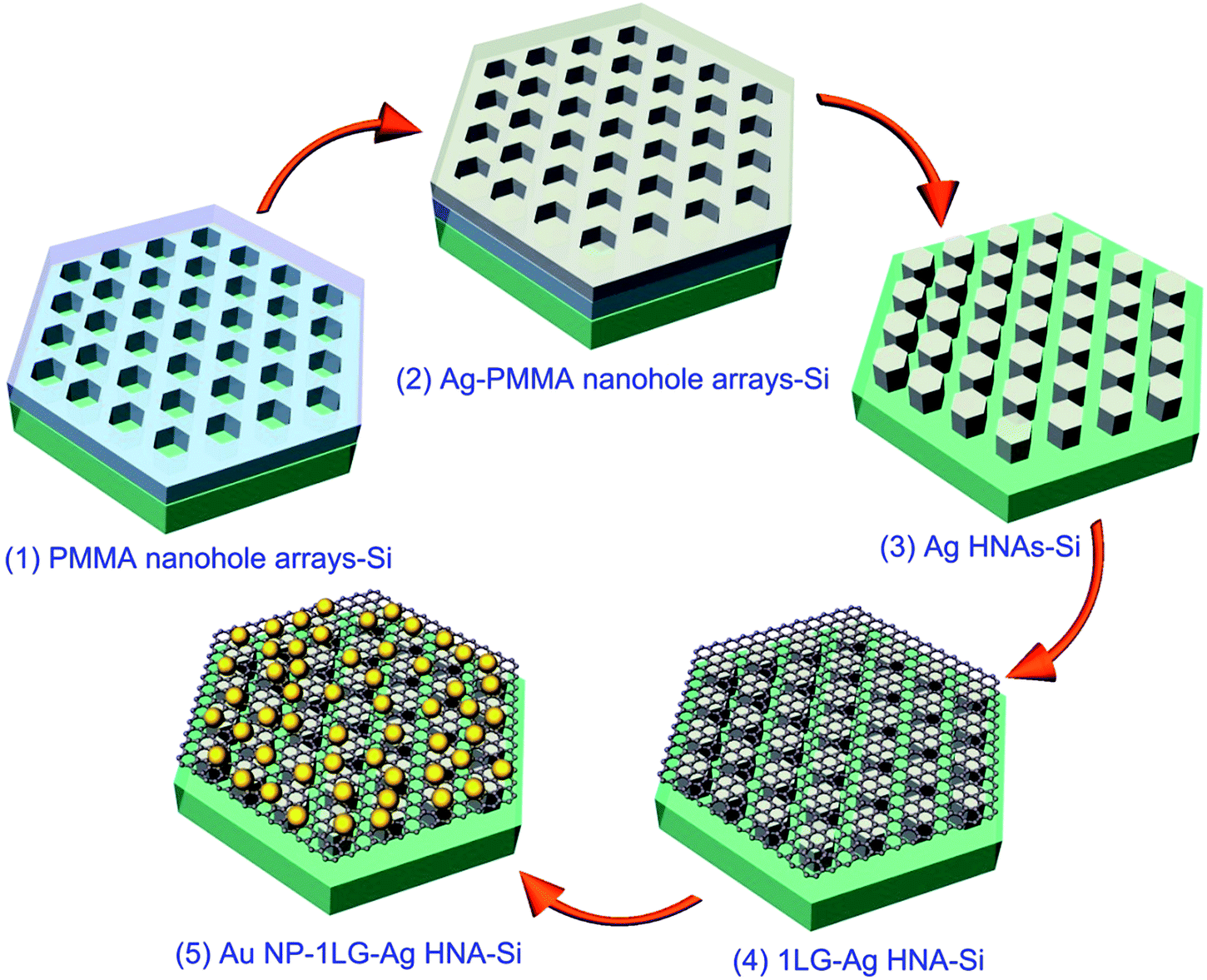 | ||
| Fig. 1 Schematics illustrating the fabrication process of Au NP–1LG–Ag HNA hybrid structure. | ||
2.2 Structural characterizations of the fabricated structures
Fig. 2 shows the scanning electron microscope (SEM) and atomic force microscopy (AFM) analyses of a typical structure sequence in accordance with the steps mentioned above. For comparison, the graphene existence or non-existence structures are depicted together. Fig. 2a is the SEM image of Ag HNAs with or without graphene covered on the surface. We can see that: (i) the patterned Ag HNAs exhibit excellent uniformity of individual Ag particle with high structural regularity; (ii) the graphene layer remains well connected after being transferred onto the Ag HNAs surface, implying the flexibility of graphene for the hybridization with ordered metal nanostructures; and (iii) the Ag hexagons covered by graphene films can still be observed clearly. The corresponding AFM images of Ag HNAs and 1LG–Ag HNA structures are shown in Fig. 2b and c, respectively, which demonstrate consistent morphological characterizations to that observed in Fig. 2a. Here, the lattice period (the distance between the adjacent hexagons in the longitudinal direction) is 175 nm. The roughness of the structures is further verified by the cross section in the AFM images (Fig. S1†), where an obvious decrease of surface roughness is observed after the coverage of graphene film on Ag HNAs surfaces.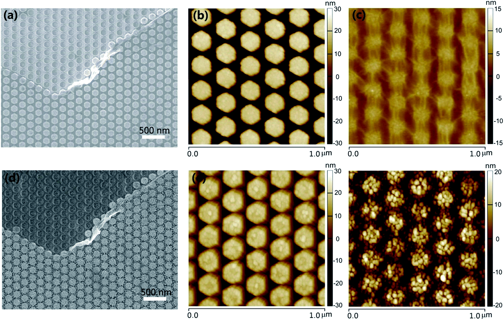 | ||
| Fig. 2 (a) SEM image of Ag HNAs without and with monolayer graphene covered on the surface. AFM images of (b) Ag HNAs and (c) 1LG–Ag HNA structures, respectively. (d) SEM image of the same area shown in (a) after a 5 nm Au layer was deposited and annealed. AFM images of (e) Au NP–Ag HNA and (f) Au NP–1LG–Ag HNA structures, respectively. The lattice periods of Ag HNAs are all 175 nm. | ||
Fig. 2d depicts the SEM image of the completely same area as that in Fig. 2a after a deposition and annealing process of 5 nm Au thin film. Obviously, Au NPs are formed and assembled on the structure surface. Here, the successful generation of Au NPs can be attributed to the spatial reactivity during the annealing process, leading to local nucleation sites and growth of small particles.21 With graphene introduced into the hybrid structure, the graphene layer functions as a 2D scaffold to anchor the top Au NPs and the bottom Ag hexagons, while the Au NPs are stacked directly on the structure surfaces for Au NP–Ag HNA structure. From the AFM image of Au NP–Ag HNA structure, we can see that the surface roughness is enlarged for the Ag hexagon surfaces after the formation of Au NPs when compared with that of bare Ag HNAs (Fig. 2e and S2†). As indicated in the AFM image of Au NP–1LG–Ag HNA hybrid system (Fig. 2f), although a slight bending and dropping of Au NPs along the profile of 1LG–Ag HNA are observed, the Au NPs remained packed closely, which imply the important supporting role of graphene for the assembly of Au NPs. The well-designed and fabricated Au NP–1LG–Ag HNA hybrid structure has taken the advantages of the strong plasmonic electric field enhancement of Ag, the chemical stability of Au and the single-atom feature and mechanical flexibility of graphene, which are all beneficial for promoting the structure SERS capability.
The precise control over the structures offers the flexibility for tailoring the plasmonic coupling of metal NPs. Exactly, the creation of sub-10 nm gaps could allow for orders of magnitude increase of the electric field enhancement.31,32 Fig. 3 depicts the AFM images of Ag HNAs without or with monolayer graphene covered on the surface for four different lattice periods. For the pattern written, the side length of Ag hexagons was fixed to be 68 nm, and the distance between the adjacent two columns was equal to the lattice period, and the thickness of Ag deposited was 50 nm. As indicated, ordered Ag HNAs with lattice period of 210 nm (Fig. 3a), 186 nm (Fig. 3b), 164 nm (Fig. 3c) and 151 nm (Fig. 3d) were obtained. As the side length of hexagons keeps consistent, the interparticle space is reduced with the decrease of period, enabling a fine-tuning of the electric field enhancement. The simulated electric field intensity distributions reveal that the electric field enhancement increases with the decrease of the interparticle space (Fig. S3†). It is worth noticing that the morphologies of the bottom Ag HNAs have an important influence on the following transfer of graphene films and assembly of Au NPs. As depicted in the AFM images, an obvious dropping along the seam of Ag hexagons and small amount of wear-and-tear were observed by placing graphene onto Ag HNAs with relatively large interparticle space (Fig. 3e and f). Moreover, some broken regions were also observed after the assembly of Au NPs (Fig. S4†). In contrast, the graphene film remains connected with excellent uniformity when it was covered on the Ag HNAs with small gaps (Fig. 3g and h). Furthermore, the structure with sub-10 nm interparticle spaces maintains excellent uniformity and non-destructive features in a large scale even after a deposition and anneal process of Au film (we will show in the following discussion).
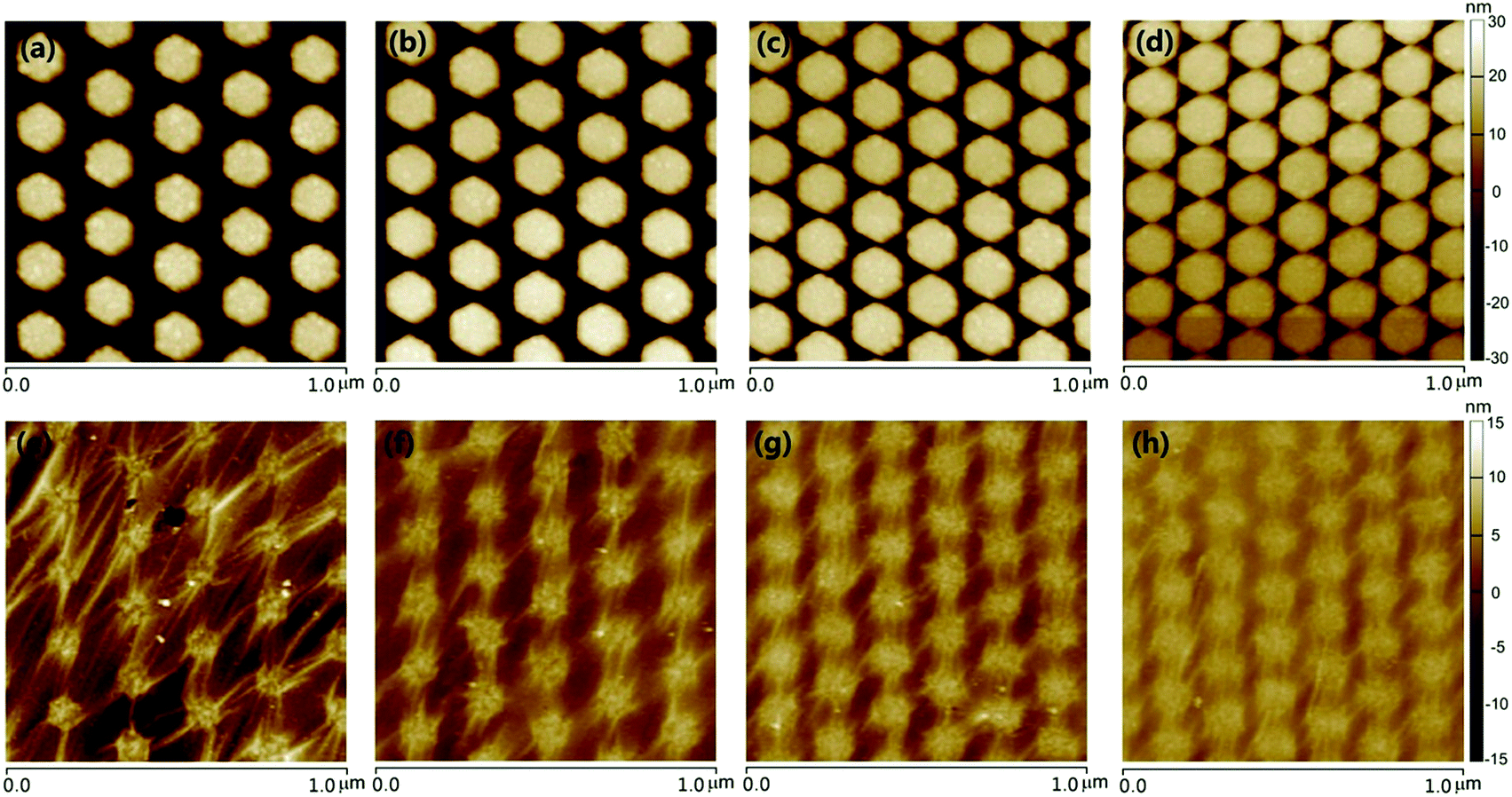 | ||
| Fig. 3 AFM images of (a–d) Ag HNAs and (e–h) 1LG–Ag HNA structures with lattice period of (a and e) 210 nm, (b and f) 186 nm, (c and g) 164 nm and (d and f) 151 nm, respectively. | ||
The findings, revealing the effective substrate-fabrication process, pave the way to further optimize the design of graphene–metal hybrid structure through structural parameters. Through a further modulation of the fabrication process, we have obtained Ag HNAs with lattice period equal to 140 nm and interparticle space bellow 10 nm. As demonstrated by the SEM and AFM images for Ag HNAs (Fig. 4a and b), high-density EM hot spots with interparticle space of ∼7 nm are created. By covering graphene onto the fabricated Ag HNAs, the graphene film maintains good completeness and flatness in a large scale (Fig. 4c and d). After the further assembly of Au NPs on 1LG–Ag HNA, 3D Au NP–1LG–Ag HNA hybrid structure is obtained (Fig. 4e and f). Here, the diameter of Au NPs is ∼20 nm and the distance between the adjacent Au NPs is ∼25 nm (Fig. S5†).
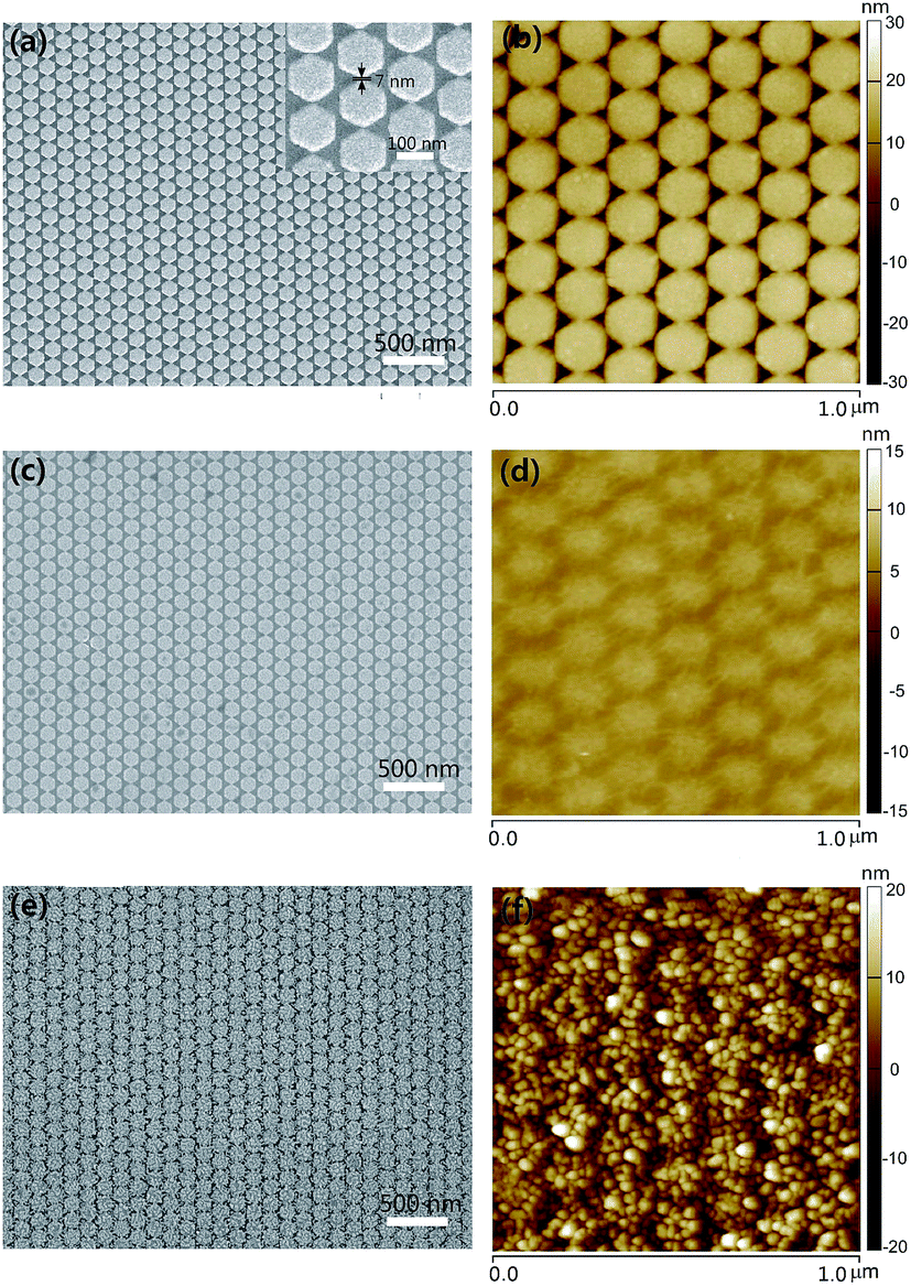 | ||
| Fig. 4 (a, c and e) SEM and (b, d and f) AFM images of (a and b) Ag HNAs, (c and d) 1LG–Ag HNA and (e and f) Au NP–1LG–Ag HNA structures with 140 nm lattice period for Ag HNAs. The enlarged view of bare Ag HNAs in (a) demonstrates that the space between the adjacent Ag hexagons is on the size of ∼7 nm. | ||
2.3 Electric field enhancement effects
To verify the plasmonic effect for the fabricated structure, we have conducted finite element method numerical simulations using Comsol Multiphysics.33–35 As shown in the simulation configuration (Fig. 5a), the side length of Ag hexagons is set to be 68 nm, the lattice period is 140 nm and the height is 50 nm. The outer edges of the hexagons were slightly rounded in order to match the shape of the actual structures. The diameter of Au NPs is taken to be 20 nm and the corresponding period is 25 nm for mimicking the average dimension of Au NPs in the experiments. The thickness of graphene interlayer between Au NPs and Ag HNAs is set to be 1 nm. A plane lightwave with a polarized electric field in the y-direction was launched normally from the top. A shared idea is that the generation of the electric field enhancement is related to the presence of metal NPs, and the magnitude of the enhanced electric field depends on the structure configurations.36 As indicated in Fig. 5b for bare Ag HNAs, the electric field is highly enhanced at the spaces between the adjacent Ag hexagons, evidencing the strong localization of the enhanced electric field. With a graphene layer coated on the surface, a similar electric filed enhancement is obtained (Fig. 5c), demonstrating a negligible attenuation of the plasmonic electric field enhancement owing to the excellent penetrability of graphene.19 In detail, the maximum of the electric field enhancements are 32 or 31 for Ag HNAs or graphene–Ag HNA, respectively. In the case of Au NP–Ag HNA structure (Fig. 5d), although some additional plasmonic electric field enhancements are observed, the maximal electric field enhancement remains 32 due to the weak coupling effect between Au NPs and Ag HNAs. As graphene is introduced between Au NPs and Ag HNAs, the Au NP–graphene–Ag HNA structure exhibits a multi-dimensional plasmonic coupling effect between the horizontal and vertical metal NPs (Fig. 5e–g). Remarkably, the hybridization of multi-scale plasmonic couplings, including Au NP–Au NP, Au NP–Ag hexagon and Ag hexagon–Ag hexagon couplings, has led to an electric field enhancement maximum of 107. As a result, the highly enhanced electric field in the 3D structure may promote extremely enhanced SERS sensing as the EM field-induced SERS enhancement is proportional to the fourth power of the EM enhancement.17,37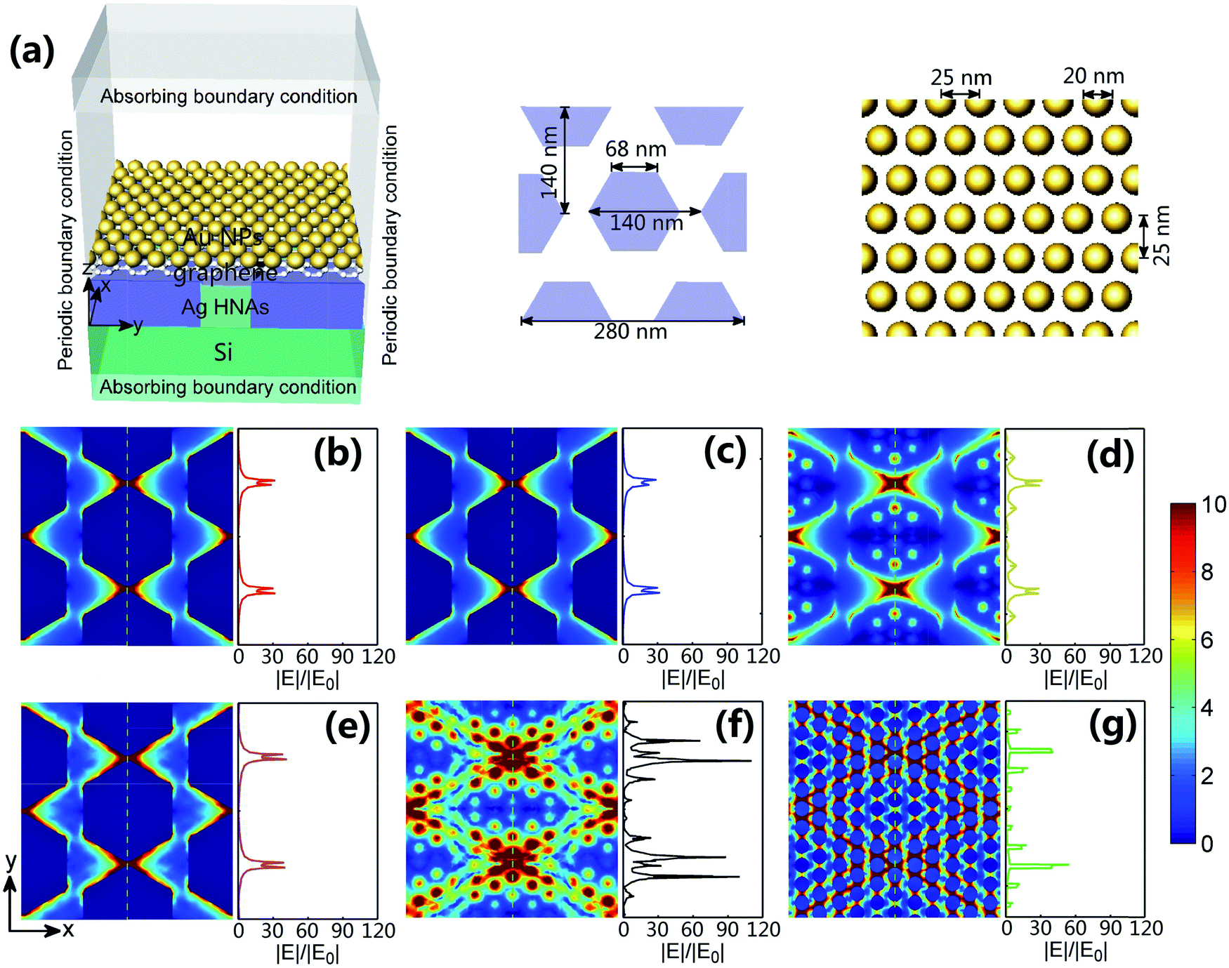 | ||
| Fig. 5 (a) Configuration of Au NP–graphene–Ag HNA on a Si substrate used for simulation. The lattice period of Ag HNAs is 140 nm, the side length of Ag hexagons is 68 nm and the thickness is 50 nm. The diameter of Au NPs is 20 nm and the distance between the adjacent Au NPs is 25 nm. The thickness of graphene film embedded between Au NPs and Ag HNAs is 1 nm. Normalized electric field intensity distributions in the xy plane for (b) bare Ag HNAs at z = 25 nm, (c) graphene–Ag HNA at z = 25 nm, (d) Au NP–Ag HNA at z = 50 nm, and Au NP–graphene–Ag HNA structure (e) inside the bottom Ag HNAs layer with z = 25 nm, (f) inside the graphene layer with z = 50.5 nm and (g) inside the top Au NPs layer with z = 61 nm, respectively. The right side of each picture plots the electric field intensity magnitude along the green dotted lines on the left. | ||
2.4 SERS detection
We first measured the SERS spectra of graphene. Fig. 6a shows the SERS spectra of graphene for the structures of 1LG–Ag HNA and Au NP–1LG–Ag HNA. For the reference, the Raman spectra of monolayer graphene covered on the Au NPs and Si substrate are also measured. Clearly, the quintessential Raman peaks of G peak around 1580 cm−1 and 2D peak around 2690 cm−1 are observed. The G peak arises from the doubly degenerate zone center E2g mode and the 2D peak denotes the second order of zone boundary phonons.38 The weak D peak around 1350 cm−1 implies the low percentage of defects for the graphene films used and few adsorbents remaining in the graphene transfer processes.39–41 The single Lorentzian lineshape of 2D peak with full width at half maximum less than 35 cm−1 expresses the feature of single layer graphene. These results indicates the successful coverage or embedding of graphene films. Compared with 1LG–Si structure, the Raman intensities of graphene for both the G and 2D bands are enhanced in other three structures for the plasmon excitation of metal NPs. Detailly, the 1LG–Au NP, 1LG–Ag HNA and Au NP–1LG–Ag HNA structures have exhibited 24-, 97- and 3107-fold stronger Raman signal for the G peak of graphene than 1LG–Si substrate (Fig. S6†). As a result, the fabricated Au NP–1LG–Ag HNA structure has exhibited ∼32-fold increase for the Raman intensity of graphene than 1LG–Ag HNA structure owing to the intensely enhanced electric field.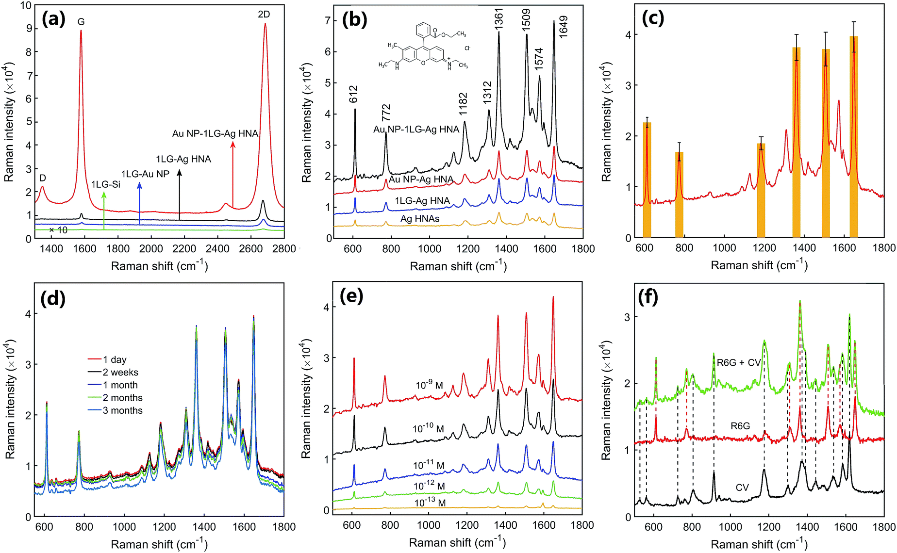 | ||
| Fig. 6 SERS characterization results of graphene and dye molecules. (a) SERS spectra of single layer graphene for the structures of 1LG–Si, 1LG–Au NP, 1LG–Ag HNA and Au NP–1LG–Ag HNA, respectively. (b) SERS spectra obtained from 10−7 M R6G decorated Au NP–1LG–Ag HNA, Au NP–Ag HNA, 1LG–Ag HNA and Ag HNAs structures. Inset is the chemical structure of R6G. (c) Large-area uniformity of the 3D Au NP–1LG–Ag HNA nanostructure coated with 10−8 M R6G molecules. Error bars indicate the standard deviations from 60 random spots. (d) Long-term stability test of the 3D Au NP–1LG–Ag HNA structure: the SERS signal of 10−8 M R6G obtained after keeping the sample in the Lab for one day, two weeks, 1 month, two months, and three months. (e) SERS spectra of R6G on Au NP–1LG–Ag HNA substrate with molecular concentrations ranging from 1 nM to 0.1 pM. (f) SERS spectra of pure aqueous solutions of 5 × 10⁻¹¹ M R6G, 1 × 10⁻¹⁰ M CV and a mixture of 5 × 10⁻¹¹ M R6G and 1 × 10⁻¹⁰ M CV. | ||
Fig. 6b shows the SERS spectra of 10−7 M R6G chemisorbed on Au NP–1LG–Ag HNA substrate. For comparison, the sensing properties of R6G on Ag HNAs, 1LG–Ag HNA and Au NP–Ag HNA structures are also researched. All the typical vibrational modes of R6G for 612, 772, 1361, 1509 and 1649 cm−1 are observed and match well with those reported previously.42 Compared to the SERS signal of R6G on Ag HNAs substrate, the 2.3-fold additional signal enhancement for the 1LG–Ag HNA substrate is accounted for the chemical enhancement of graphene due to π–π interactions and charge transfer between graphene and R6G molecules. Importantly, the 3D Au NP–1LG–Ag HNA structure has generated 11.3- or 4.9-fold stronger Raman signal when compared with Ag HNAs or 1LG–Ag HNA structure, respectively. Compared to the case of Au NP–Ag HNA substrate, 4.1-fold SERS signal enhancement was obtained in the Au NP–1LG–Ag HNA hybrid system. Besides the chemical enhancement, the highly intensified SERS intensity for the Au NP–1LG–Ag HNA hybrid structure can be attributed to the creation of high-density hot spots with dramatically enhanced electric field.
By measuring the SERS signal of 10−8 M R6G from 60 randomly selected spots on Au NP–1LG–Ag HNA platform, the relative standard deviation (RSD) was calculated to be ∼7.3%, evidencing the excellent SERS signal uniformity and reproducibility (Fig. 6c and S7†). We have measured the SERS signal of R6G on 3D Au NP–1LG–Ag HNA substrate for different time. As indicated in Fig. 6d, it only brings a decrease of 5.7% after the sample was stored for 3 months, manifesting the stability of the prepared 3D structures. Furthermore, we achieved R6G SERS detection with concentration down to 0.1 pM (equivalent to ∼0.015 molecules per μm2 of the surface area) for the 3D Au NP–1LG–Ag HNA substrate (Fig. 6e and S8†). As a result, the elaborately-designed and well-fabricated Au NP–1LG–Ag HNA platform has facilitated the development and practical application of SERS substrates with high sensitivity, good reproducibility and strong stability. Here, we demonstrated that the prepared 3D structure can detect bi-analytes of R6G and CV in a solution. As indicated in Fig. 6f, the vibrational bands of R6G (612, 1361, 1509 and 1649 cm−1) and the Raman peaks of CV (915, 1172, 1372 and 1619 cm−1) were observed simultaneously in a mixture aqueous solution of 5 × 10⁻¹¹ M R6G and 1 × 10⁻¹⁰ M CV. This demonstrates a promising potential for the practical monitoring of pollutants in the real environment.
3. Conclusions
In conclusion, we have developed an approach to integrate EM enhancement and chemical enhancement for enhanced SERS performance based on graphene–plasmonic hybrids. The as-prepared 3D Au NP–1LG–Ag HNA hybrid system has enabled the SERS analysis with high sensitivity, good uniformity, reliability and stability. Remarkably, 3107-fold enhancement for the Raman response of graphene and a limit as low as 0.1 pM for R6G were obtained by using the 3D hybrid structure. Furthermore, the 3D SERS substrate has facilitated the simultaneous detection of both R6G and CV molecules. The strategy used in this work has enabled the fabrication of high-activity SERS substrate with excellent flexibility by making full use of the multi-functional roles of graphene and structure-tunability of metal nanostructures. The concept demonstrated here should be extended to the fabrication of other 2D material–plasmonic hybrid platform with further modifications on structures and fabrication techniques. This work represents a step towards the fabrication of SERS substrate with high-sensitivity and strong-reproducibility, and opens a new avenue for rationally designing plasmonic–graphene hybrid structures for SERS sensing.4. Experimental section
4.1 Preparation of 3D Au NP–1LG–Ag HNA hybrid structure
The Ag HNAs are fabricated by e-beam writing of hexagon arrays on PMMA resist, deposition of Ag film and a followed lift-off process. In a standard process, a thin layer of PMMA (∼260 nm thickness) was first spin-coated onto Si wafer at 3500 rpm for 60 s and backed at 180 °C for 90 s on a hot plate to evaporate the solvent in the resist and form a harder coating. Subsequently, a hexagon-shaped array pattern was written using an EBL machine (JEOL JBX-6300FS) with an area dosage of 800 μC cm−2 and a current of 100 pA. The sample was immersed into a solution of methyl isobutyl ketone (MIBK) and isopropanol (IPA) in a 1![[thin space (1/6-em)]](https://www.rsc.org/images/entities/char_2009.gif) :3 mixture ratio for 60 s for developing, rinsed in IPA for 60 s, and followed with a gentle N2 blowing to form a PMMA HNA pattern.43,44 A 5 nm-thick Cr adhesion layer and 50 nm-thick Ag layer were sputtered onto the sample surface sequentially at rates of 0.5 Å s−1 under the pressure of about 10−4 mbar by magnetic sputtering. After the sample was immersed into acetone to process lift-off, wherein the excess resist and metal film on top of PMMA were removed, the ordered Ag–Gr HNAs were obtained. For simplicity, we call it Ag HNAs. In the next step, single layer graphene film was transferred onto the Ag HNAs to construct 1LG–Ag HNA structure. A PMMA layer (∼300 nm thickness) was spin-coated onto the graphene films on Cu foils and dried at 150 °C on a hot plate.45,46 The PMMA–graphene–Cu foil was immersed in ammonium persulfate (0.07 g ml−1) to etch away Cu, followed with a washing with deionized water, and then transferred onto Ag HNAs. The sample was immersed in acetone to dissolve PMMA for achieving 1LG–Ag HNA structure. Finally, a layer of 5 nm Au film was deposited onto the as-prepared 1LG–Ag HNA at a rate of 0.1 Å s−1 by magnetic sputtering and annealed in Ar at 300 °C for 60 min with a heating rate of 5 °C min−1, thereby forming 3D Au NP–1LG–Ag HNA hybrid structure.
:3 mixture ratio for 60 s for developing, rinsed in IPA for 60 s, and followed with a gentle N2 blowing to form a PMMA HNA pattern.43,44 A 5 nm-thick Cr adhesion layer and 50 nm-thick Ag layer were sputtered onto the sample surface sequentially at rates of 0.5 Å s−1 under the pressure of about 10−4 mbar by magnetic sputtering. After the sample was immersed into acetone to process lift-off, wherein the excess resist and metal film on top of PMMA were removed, the ordered Ag–Gr HNAs were obtained. For simplicity, we call it Ag HNAs. In the next step, single layer graphene film was transferred onto the Ag HNAs to construct 1LG–Ag HNA structure. A PMMA layer (∼300 nm thickness) was spin-coated onto the graphene films on Cu foils and dried at 150 °C on a hot plate.45,46 The PMMA–graphene–Cu foil was immersed in ammonium persulfate (0.07 g ml−1) to etch away Cu, followed with a washing with deionized water, and then transferred onto Ag HNAs. The sample was immersed in acetone to dissolve PMMA for achieving 1LG–Ag HNA structure. Finally, a layer of 5 nm Au film was deposited onto the as-prepared 1LG–Ag HNA at a rate of 0.1 Å s−1 by magnetic sputtering and annealed in Ar at 300 °C for 60 min with a heating rate of 5 °C min−1, thereby forming 3D Au NP–1LG–Ag HNA hybrid structure.
4.2 Structural characterization and SERS measurement
The morphologies of the samples were characterized using SEM (JSM-6700F) and AFM (BRUKER Dimension Icon). Raman spectra were measured using Renishaw inVia Raman Microscope with a laser wavelength of 532 nm and 1800 line per mm grating. For measuring the Raman signals of dye molecules, a 10 μl droplet was dispersed on the substrates prepared and dried in air. Here, R6G solutions with different concentrations were obtained by dissolving the solid powders and diluting using deionized water. The mixture solution of R6G and CV were obtained by dissolving the R6G and CV powders in deionized water. The laser power was kept 5 mW for measuring graphene and 0.5 mW for measuring molecules to avoid sample heating and photo-induced damages. The integration time is 10 s for measuring the Raman spectra of graphene for 1LG–Si and 1 s for other measurements. A ×50 objective was used and the laser spot was ∼1 μm2. The Raman spectra were processed by WiRE 4.3 Raman software.4.3 Finite element numerical simulations
The software package “Comsol Multiphysics” was used in the simulations, which is based on finite element method to solve Maxwell's equations.25,33,35 For the simulation configuration (Fig. 5a), the side length of Ag hexagons was 68 nm, and the distance between the adjacent Ag hexagons in the y-direction is equal to the distance between the adjacent two rows in the x-direction. The outer edges of the hexagons were slightly rounded in order to match the shape of the actual structures. The thickness of graphene films was 1 nm, which is reasonable for CVD-grown graphene by considering the inhomogeneity in the growth and transfer processes.17 The diameter of Au NPs is 20 nm and the distance between the adjacent Au NPs is 25 nm for mimicking the average size of Au NPs obtained. The lateral and longitudinal dimensions of the unite cell simulated are both 280 nm. In the horizontal directions, periodic boundary conditions were set for simulating a single unite cell, and in the vertical direction, the perfectly-matched-layer was used for eliminating the undesired reflections from boundaries. The incident wavelength was set to be 532 nm with the electric field polarized along the y-axis. The optical parameters of Au and Ag were given by Drude model,47 the refractive index of graphene was calculated using the formula n = 3 + c1(λ/3)i (c1 = 5.446 μm−1 and λ was the wavelength), and the dielectric constant of Si was 13.39.48 Convergence mesh analysis was used for achieving stationary results, and the mesh maximum element size was set as 0.2 nm in the domains representing graphene, 3 nm in Au NPs, 6 nm in Ag hexagons and 10 nm for all the elements in the air and substrate subdomains.Acknowledgements
This work was partially carried out at the USTC Center for Micro and Nanoscale Research and Fabrication, and we thank Chenggang Zhou, Kun Zhang, Dianfa Zhou, Jinlan Peng, Xiuxia Wang, Linjun Wang and Haibin Zhang for their technical support. We appreciate the financial support from the Natural Science Foundation of Shandong Province (ZR2016EMP01), Innovation Project of Ludong University (LA 2016003), the National Natural Science Foundation of China (11504155) and the National Basic Research Program of China (2012CB922001).Notes and references
- A. K. Geim, Science, 2009, 324, 1530–1534 CrossRef CAS PubMed.
- K. S. Novoselov, A. K. Geim, S. V. Morozov, D. Jiang, Y. Zhang, S. V. Dubonos, I. V. Grigorieva and A. A. Firsov, Science, 2004, 306, 666–669 CrossRef CAS PubMed.
- H. Yan, T. Low, W. Zhu, Y. Wu, M. Freitag, X. Li, F. Guinea, P. Avouris and F. Xia, Nat. Photonics, 2013, 7, 394–399 CrossRef CAS.
- T. Wu, X. Zhang, Q. Yuan, J. Xue, G. Lu, Z. Liu, H. Wang, H. Wang, F. Ding, Q. Yu, X. Xie and M. Jiang, Nat. Mater., 2016, 15, 43–47 CrossRef CAS PubMed.
- X. Li, W. Zhong, P. Cui, J. Li and J. Jiang, J. Phys. Chem. Lett., 2016, 7, 1750–1755 CrossRef CAS PubMed.
- L. Kang, J. Chu, H. Zhao, P. Xu and M. Sun, J. Mater. Chem. C, 2015, 3, 9024–9037 RSC.
- X. Ling, L. Xie, Y. Fang, H. Xu, H. Zhang, J. Kong, M. S. Dresselhaus, J. Zhang and Z. Liu, Nano Lett., 2010, 10, 553–561 CrossRef CAS PubMed.
- W. Xu, N. Mao and J. Zhang, Small, 2013, 9, 1206–1224 CrossRef CAS PubMed.
- A. Otto, I. Mrozek, H. Grabhorn and W. Akemann, J. Phys.: Condens. Matter, 1992, 4, 1143–1212 CrossRef CAS.
- K. A. Willets, Chem. Soc. Rev., 2014, 43, 3854–3864 RSC.
- S. Yang, X. Dai, B. B. Stogin and T.-S. Wong, Proc. Natl. Acad. Sci. U. S. A., 2016, 113, 268–273 CrossRef CAS PubMed.
- G. Bodelon, V. Montes-Garcia, V. Lopez-Puente, E. H. Hill, C. Hamon, M. N. Sanz-Ortiz, S. Rodal-Cedeira, C. Costas, S. Celiksoy, I. Perez-Juste, L. Scarabelli, A. La Porta, J. Perez-Juste, I. Pastoriza-Santos and L. M. Liz-Marzan, Nat. Mater., 2016, 15, 1203–1211 CrossRef CAS PubMed.
- X. Ling, S. Huang, S. Deng, N. Mao, J. Kong, M. S. Dresselhaus and J. Zhang, Acc. Chem. Res., 2015, 48, 1862–1870 CrossRef CAS PubMed.
- X. Li, J. Zhu and B. Wei, Chem. Soc. Rev., 2016, 45, 3145–3187 RSC.
- Y. Zhao and Y. Zhu, Nanoscale, 2015, 7, 14561–14576 RSC.
- X. Li, W. Zhong, P. Cui, J. Li and J. Jiang, J. Phys. Chem. Lett., 2016, 7, 1750–1755 CrossRef CAS PubMed.
- X. Zhu, L. Shi, M. S. Schmidt, A. Boisen, O. Hansen, J. Zi, S. Xiao and N. A. Mortensen, Nano Lett., 2013, 13, 4690–4696 CrossRef CAS PubMed.
- Y. Du, Y. Zhao, Y. Qu, C.-H. Chen, C.-M. Chen, C.-H. Chuang and Y. Zhu, J. Mater. Chem. C, 2014, 2, 4683–4691 RSC.
- W. Xu, X. Ling, J. Xiao, M. S. Dresselhaus, J. Kong, H. Xu, Z. Liu and J. Zhang, Proc. Natl. Acad. Sci. U. S. A., 2012, 109, 9281–9286 CrossRef CAS PubMed.
- Y. B. Zhang, Y. W. Tan, H. L. Stormer and P. Kim, Nature, 2005, 438, 201–204 CrossRef CAS PubMed.
- K. J. Lee, D. Kim, B. C. Jang, D.-J. Kim, H. Park, D. Y. Jung, W. Hong, T. K. Kim, Y.-K. Choi and S.-Y. Choi, Adv. Funct. Mater., 2016, 26, 5093–5101 CrossRef CAS.
- J. Zhao, M. Sun, Z. Liu, B. Quan, C. Gu and J. Li, Sci. Rep., 2015, 5, 16019 CrossRef CAS PubMed.
- J. Wu, Y. Xu, P. Xu, Z. Pan, S. Chen, Q. Shen, L. Zhan, Y. Zhang and W. Ni, Nanoscale, 2015, 7, 17529–17537 RSC.
- A. Liu, T. Xu, J. Tang, H. Wu, T. Zhao and W. Tang, Electrochim. Acta, 2014, 119, 43–48 CrossRef CAS.
- Y. Zhao, X. Li, Y. Du, G. Chen, Y. Qu, J. Jiang and Y. Zhu, Nanoscale, 2014, 6, 11112–11120 RSC.
- W. Xu, J. Xiao, Y. Chen, Y. Chen, X. Ling and J. Zhang, Adv. Mater., 2013, 25, 928–933 CrossRef CAS PubMed.
- S. Carrasco, V. Canalejas-Tejero, F. Navarro-Villoslada, C. A. Barrios and M. C. Moreno-Bondi, J. Mater. Chem. C, 2014, 2, 1400–1403 RSC.
- M. Chirumamilla, A. Toma, A. Gopalakrishnan, G. Das, R. P. Zaccaria, R. Krahne, E. Rondanina, M. Leoncini, C. Liberale, F. De Angelis and E. Di Fabrizio, Adv. Mater., 2014, 26, 2353–2358 CrossRef CAS PubMed.
- X. Li, W. Cai, J. An, S. Kim, J. Nah, D. Yang, R. Piner, A. Velamakanni, I. Jung, E. Tutuc, S. K. Banerjee, L. Colombo and R. S. Ruoff, Science, 2009, 324, 1312–1314 CrossRef CAS PubMed.
- B. Luo, H. Liu, L. Jiang, L. Jiang, D. Geng, B. Wu, W. Hu, Y. Liu and G. Yu, J. Mater. Chem. C, 2013, 1, 2990–2995 RSC.
- Z. Zhou, Z. Zhao, Y. Yu, B. Ai, H. Möhwald, R. C. Chiechi, J. K. W. Yang and G. Zhang, Adv. Mater., 2016, 28, 2956–2963 CrossRef CAS PubMed.
- C. Zhu, G. Meng, P. Zheng, Q. Huang, Z. Li, X. Hu, X. Wang, Z. Huang, F. Li and N. Wu, Adv. Mater., 2016, 28, 4871–4876 CrossRef CAS PubMed.
- COMSOL 4.3a Reference Manual, 2012, 4.3.
- Y. Zhao, G. Chen, Y. Du, J. Xu, S. Wu, Y. Qu and Y. Zhu, Nanoscale, 2014, 6, 13754–13760 RSC.
- T.-T. Zhuang, Y. Liu, Y. Li, Y. Zhao, L. Wu, J. Jiang and S.-H. Yu, Angew. Chem., Int. Ed., 2016, 55, 6396–6400 CrossRef CAS PubMed.
- J. W. Jeong, M. M. P. Arnob, K.-M. Baek, S. Y. Lee, W.-C. Shih and Y. S. Jung, Adv. Mater., 2016, 28, 8695–8704 CrossRef CAS PubMed.
- H. Ko, S. Singamaneni and V. V. Tsukruk, Small, 2008, 4, 1576–1599 CrossRef CAS PubMed.
- A. C. Ferrari, J. C. Meyer, V. Scardaci, C. Casiraghi, M. Lazzeri, F. Mauri, S. Piscanec, D. Jiang, K. S. Novoselov, S. Roth and A. K. Geim, Phys. Rev. Lett., 2006, 97, 187401 CrossRef CAS PubMed.
- G. Xu, J. Liu, Q. Wang, R. Hui, Z. Chen, V. A. Maroni and J. Wu, Adv. Opt. Mater., 2012, 24, OP71–OP76 CrossRef CAS PubMed.
- X. Liu, J. Wang, Y. Wu, T. Fan, Y. Xu, L. Tang and Y. Ying, Sci. Rep., 2015, 5, 17167 CrossRef CAS PubMed.
- P. Klar, E. Lidorikis, A. Eckmann, I. A. Verzhbitskiy, A. C. Ferrari and C. Casiraghi, Phys. Rev. B: Condens. Matter Mater. Phys., 2013, 87, 205435 CrossRef.
- G. Lu, H. Li, C. Liusman, Z. Yin, S. Wu and H. Zhang, Chem. Sci., 2011, 2, 1817–1821 RSC.
- R. Palankar, N. Medvedev, A. Rong and M. Delcea, ACS Nano, 2013, 7, 4617–4628 CrossRef CAS PubMed.
- N. A. Abu Hatab, J. M. Oran and M. J. Sepaniak, ACS Nano, 2008, 2, 377–385 CrossRef CAS PubMed.
- J. Song, F.-Y. Kam, R.-Q. Png, W.-L. Seah, J.-M. Zhuo, G.-K. Lim, P. K. H. Ho and L.-L. Chua, Nat. Nanotechnol., 2013, 8, 356–362 CrossRef CAS PubMed.
- A. Reina, H. Son, L. Jiao, B. Fan, M. S. Dresselhaus, Z. Liu and J. Kong, J. Phys. Chem. C, 2008, 112, 17741–17744 CAS.
- E. J. Zeman and G. C. Schatz, J. Phys. Chem., 1987, 91, 634–643 CrossRef CAS.
- M. Bruna and S. Borini, Appl. Phys. Lett., 2009, 94, 031901 CrossRef.
Footnote |
| † Electronic supplementary information (ESI) available. See DOI: 10.1039/c6ra27973b |
| This journal is © The Royal Society of Chemistry 2017 |