
 Open Access Article
 This Open Access Article is licensed under a
 Creative Commons Attribution 3.0 Unported Licence
Semiconducting/insulating polymer blends with dual phase separation for organic field-effect transistors†
Jung Hun Leea,
Young Hun Leeb,
Yeon Hee Hac,
Jaehyuk Kwond,
Seungmoon Pyod,
Yun-Hi Kim *c and
Wi Hyoung Lee*a
*c and
Wi Hyoung Lee*a
aDepartment of Organic and Nano System Engineering, Konkuk University, Seoul 143-701, Korea. E-mail: whlee78@konkuk.ac.kr; Fax: +82-2-457-8895; Tel: +82-2-450-3468
bSchool of Advanced Materials Science and Engineering, Sungkyunkwan University, Suwon 440-746, Korea
cDepartment of Chemistry and RINS, Gyeongsang National University, Jinju, 660-701, Korea. E-mail: ykim@gnu.ac.kr
dDepartment of Chemistry, Konkuk University, 120 Neungdong-ro, Gwangjin-gu, Seoul 143-701, Korea
First published on 23rd January 2017
Abstract
In this study, diketopyrrolopyrrole (DPP)-based semiconducting polymers with alkyl chain spacers of different lengths (C24 and C29) were used to compare the effects of crystalline nature in semiconducting polymer on the phase-separation and electrical properties of DPP-based semiconducting polymer/poly(methyl methacrylate) (PMMA) blends. Hierarchical structures containing ultrathin-film (bottom) and hairy rods (top) of DPP-based semiconducting polymers formed on the substrates due to the combined effects of the self-stratification and Marangoni-instability during the phase-separation of polymer blends. In particular, 24-DPP-TVT/PMMA blend film formed-fewer and bigger semiconductor rods, because of coarsening of 24-DPP-TVT phase during solvent evaporation. In contrast, highly crystalline nature of 29-DPP-TVT prevented the coarsening of the 29-DPP-TVT rods, thereby resulted in densely packed semiconductor rods. According to the crystalline natures in DPP-based semiconducting polymers, 29-DPP-TVT phase in 29-DPP-TVT/PMMA blend exhibited lower angular spread in molecular orientation compared to 24-DPP-TVT phase in 24-DPP-TVT/PMMA blend. Accordingly, 29-DPP-TVT/PMMA field-effect transistors (FETs) exhibited significantly higher electrical properties than those of 24-DPP-TVT/PMMA FETs. In addition, field-effect mobility of 29-DPP-TVT/PMMA FETs is comparable to those of homo 29-DPP-TVT FETs, whereas the partial passivation effect lowers turn-on voltage of 29-DPP-TVT/PMMA FETs. This study that utilized dual phase-separation would provide possible guidelines for the selection of semiconducting polymer for the use of semiconducting/insulating polymer blends in FETs.
1. Introduction
Organic field-effect transistors (OFETs) based on semiconducting polymers have received much attention owing to several key merits such as solution process-ability and mechanical flexibility of semiconducting polymers. In addition, electrical performances of semiconducting polymers now exceed those of thermally evaporated organic semiconductors such as pentacene. For example, recently developed diketopyrrolopyrrole (DPP)-based donor–acceptor (D–A) polymers exhibited high field-effect mobility of >10 cm2 V−1 s−1.1–4 In this regard, DPP-based semiconducting polymers are considered as benchmark organic semiconductors ready for commercialization in switching elements in the future display. The outstanding performances of DPP-based semiconducting polymers mainly originated from the polar nature of D–A blocks with efficient intramolecular charge transport.5 In contrast, recent report of side chain engineering in DPP-based polymers indicates that intermolecular stacking can be finely tuned by changing alkyl side chains.3 Especially, long-branched side chains are beneficial for optimizing π–π stacking and accelerating the intermolecular charge transport.In addition to molecular design, decreasing cost of semiconducting polymers is a prerequisite for the commercialization. Semiconducting polymers are rather expensive, as their synthesis involves many steps under rigorous conditions. In this regard, semiconducting/insulating polymer blend can provide a route for reducing cost of the materials.6–12 Because charge transport is disturbed by an insulating component, inducing vertical phase-separation in polymer blends is necessary for guaranteeing lateral charge transport in field-effect transistors (FETs).13–15 So far vertical phase separation has been successfully demonstrated in polythiophene/insulating polymer blends.8,14 Notably, vertical phase separation can occur under well-controlled conditions such as solubility, surface energy, and substrate wetting controls. Thus, lateral phase-separation is much more common in polymer/polymer blends because of Marangoni-like instability.11,16–18 To this end, utilization of laterally phase-separated structure in the active layer of OFETs is necessary for extending the use of semiconducting/insulating polymer blends. Recent work by Cheng et al. utilized laterally phase separated polythiophene/insulating polymer blend as an active layer in OFETs.18 On that report, continuous polythiophene domains provide sites for efficient charge transport where insulating polymer domains block leakage current.
Another interesting point in semiconducting/insulating polymer blends is the effect of crystalline nature of polymers on phase-separation behaviors, thereby affecting electrical properties of OFETs. Goffri et al. successfully demonstrated that the use of insulating polymer with semicrystalline nature (i.e., isotactic polystyrene) is beneficial for increasing vertical phase-separation of semiconducting/insulating polymer blends.8 This crystallization induced phase-segregation led to high field-effect mobility with reduced use of semiconducting polymer. Notwithstanding their successful finding, they used poly(3-hexylthiophene) (P3HT) semiconducting polymer, exhibiting low crystalline film with a relatively low field-effect mobility.19 Thus, examining the effects of crystalline nature in semiconducting polymers on the phase-separation and electrical properties of semiconducting/insulating polymer blends will be very interesting. We noticed that intermolecular π–π interaction and molecular ordering of semiconducting polymers can be easily tuned by side chain engineering in DPP-based semiconducting polymers.3,20,21
In this study, DPP-based semiconducting polymers, poly[2,5-bis(2-decyltetradecyl)pyrrolo[3,4-c]pyrrole-1,4-(2H,5H)-dione-(E)-1,2-di(2,2′-bithiophen-5-yl)ethene], 24-DPP-TVT and 29-DPP-TVT were used (Fig. 1a).3 29-DPP-TVT thin film exhibited higher molecular ordering than 24-DPP-TVT thin film mainly due to the increased π–π interaction in longer alkyl chain spacer. 24-DPP-TVT and 29-DPP-TVT with different crystalline natures were blended with an insulating polymer, poly(methyl methacrylate) (PMMA), and the phase-separation behaviors as well as structural development of the resulting blends were examined. Finally, the electrical properties of FETs based on 24-DPP-TVT/PMMA and 29-DPP-TVT/PMMA blends were investigated for comparing the effects of crystalline nature in semiconducting polymers.
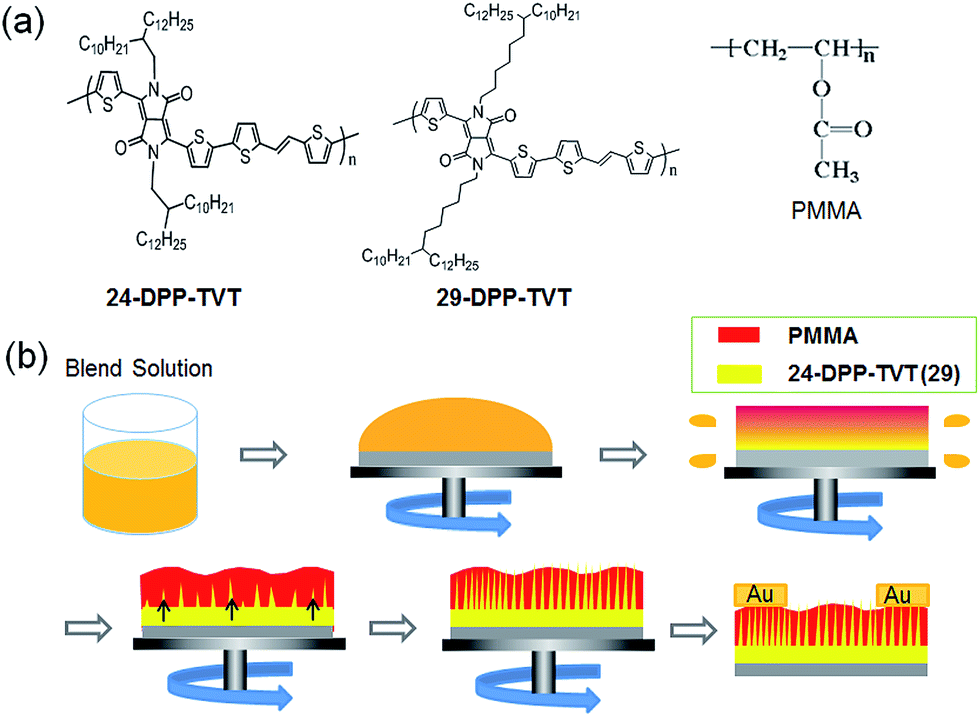 | ||
| Fig. 1 (a) Chemical structures of 24-DPP-TVT, 29-DPP-TVT, and PMMA, (b) schematic representation showing thin-film formation of the 24-DPP-TVT (29-DPP)/PMMA blend solution during solvent evaporation. | ||
2. Experimental
24-DPP-TVT (Mn = 31![[thin space (1/6-em)]](https://www.rsc.org/images/entities/char_2009.gif) 900, Mw = 54230, PDI = 1.7) and 29-DPP-TVT (Mn = 33369, Mw = 60781, PDI = 1.82) were synthesized following the procedure by Kang et al.3 The crude polymers were purified with soxhlet extraction, and final polymers (24-DPP-TVT and 29-DPP-TVT) were obtained by precipitation of the chloroform solution in methanol. PMMA (Mw = 996 kg mol−1), chlorobenzene and acetic acid were purchased from Aldrich Chemical Co. 24-DPP-TVT (or 29-DPP-TVT) solution in chlorobenzene (total concentration of 8 mg mL−1) and 24-DPP-TVT (or 29-DPP-TVT):PMMA (1:3 mass ratio) blend solution in chlorobenzene (total concentration of 8 mg mL−1) were spin-casted on SiO2 (thickness of 300 nm)/Si substrates, treated with octadecyltrichlorosilane (ODTS) prior to use. Excess solvent was completely removed by keeping the samples in a vacuum oven, and then Au source/drain electrodes were thermally evaporated on 24-DPP-TVT (or 29-DPP-TVT) film and 24-DPP-TVT (or 29-DPP-TVT)/PMMA blend film. The channel length and width of the fabricated FETs were 150 and 1500 μm, respectively. Atomic Force Microscopy (Park Scientific Instrument, Autoprobe-PC) was used to characterize the surface morphologies of the thin films. The blend films were treated overnight with acetic acid to selectively etch the PMMA layer on the top surface. Two-dimensional grazing-incidence X-ray diffraction (2D-GIXRD) patterns were obtained in Pohang Accelerator Laboratory of Korea (9A and 3C beamlines) to characterize the molecular orientation of the thin films. Electrical properties of the fabricated FETs under vacuum were characterized using Keithley 4200-SCS Source Measure Unit.
900, Mw = 54230, PDI = 1.7) and 29-DPP-TVT (Mn = 33369, Mw = 60781, PDI = 1.82) were synthesized following the procedure by Kang et al.3 The crude polymers were purified with soxhlet extraction, and final polymers (24-DPP-TVT and 29-DPP-TVT) were obtained by precipitation of the chloroform solution in methanol. PMMA (Mw = 996 kg mol−1), chlorobenzene and acetic acid were purchased from Aldrich Chemical Co. 24-DPP-TVT (or 29-DPP-TVT) solution in chlorobenzene (total concentration of 8 mg mL−1) and 24-DPP-TVT (or 29-DPP-TVT):PMMA (1:3 mass ratio) blend solution in chlorobenzene (total concentration of 8 mg mL−1) were spin-casted on SiO2 (thickness of 300 nm)/Si substrates, treated with octadecyltrichlorosilane (ODTS) prior to use. Excess solvent was completely removed by keeping the samples in a vacuum oven, and then Au source/drain electrodes were thermally evaporated on 24-DPP-TVT (or 29-DPP-TVT) film and 24-DPP-TVT (or 29-DPP-TVT)/PMMA blend film. The channel length and width of the fabricated FETs were 150 and 1500 μm, respectively. Atomic Force Microscopy (Park Scientific Instrument, Autoprobe-PC) was used to characterize the surface morphologies of the thin films. The blend films were treated overnight with acetic acid to selectively etch the PMMA layer on the top surface. Two-dimensional grazing-incidence X-ray diffraction (2D-GIXRD) patterns were obtained in Pohang Accelerator Laboratory of Korea (9A and 3C beamlines) to characterize the molecular orientation of the thin films. Electrical properties of the fabricated FETs under vacuum were characterized using Keithley 4200-SCS Source Measure Unit.
3. Results and discussion
Fig. 1b shows the schematic drawing of structural development in spin-cast 24-DPP-TVT/PMMA or 29-DPP-TVT/PMMA blend films. When 24-DPP-TVT (or 29-DPP-TVT) (1): PMMA (3) blend solution in chlorobenzene was spin-casted on ODTS-treated SiO2/Si substrate, 24-DPP-TVT (or 29-DPP-TVT) with low solubility solidified first. In addition, the formation of a hydrophilic PMMA layer at the bottom was suppressed by hydrophobic ODTS-treated SiO2/Si substrate.22 Thus, transient wetting layer consisting of PMMA-rich phase at the top and 24-DPP-TVT (or 29-DPP-TVT)-rich phase at the bottom forms during solvent evaporation. This vertically phase-separated transient wetting layer is unstable due to the Marangoni-instability.11,16 Concentration gradient-induced flow throughout the wetting layer formed laterally phase separated structure as schematically shown in Fig. 1b bottom images.Phase separated structures of 24-DPP-TVT/PMMA and 29-DPP-TVT/PMMA blend films were examined by analyzing surface morphologies in the AFM images (Fig. 2a and b). Both the images exhibited bumpy and irregular structures. Interestingly, isolated holes were regularly observed in 24-DPP-TVT/PMMA and 29-DPP-TVT/PMMA blend films, and the number of the isolated holes increased in 29-DPP-TVT/PMMA blend film. To reveal the phase-separated structure of semiconducting polymer, PMMA was selectively etched with acetic acid, which does not dissolve semiconducting polymer, 24-DPP-TVT or 29-DPP-TVT. Fig. 2c and d show phase-separated structures of 24-DPP-TVT and 29-DPP-TVT components from the blend films, respectively. Hairy rods were observed in both the height images; however, fewer and bigger semiconductor rods were detected in the etched 24-DPP-TVT/PMMA film. In particular, 24-DPP-TVT rods have diameters of 1 μm, whereas 29-DPP-TVT rods have diameters of 20 nm. Concentration gradient-induced flow throughout the wetting layer resulted in these hairy rod structures. The different phase-separated dimensions were related to the crystalline behaviors of 24-DPP-TVT or 29-DPP-TVT as discussed in the following paragraph. Although bumpy structures containing hairy rods were detected in height images (left column) and 3D profiles (inset), phase images in right column show negligible phase contrasts. This result implies that ultrathin DPP-polymer layer formed at the film-substrate interface by self-stratification. Note that phase contrast image is determined by the hardness of the materials and uniform phase images reflect the formation of uniform DPP-polymer layer at the bottom (see schematic drawings in Fig. 2 insets). When we measured thickness of remaining DPP-polymer by scratching DPP-polymer with a knife (see ESI Fig. S1†), ultrathin DPP-polymer layer with thickness of 6–7 nm fully covers the ODTS modified SiO2/Si substrate. On the other hand, thickness of bumpy rods was measured to be ∼30 nm. Thus, it is confirmed that hierarchical structures containing ultrathin-film (bottom) and hairy rods (top) of DPP-based semiconducting polymers formed on the substrates due to the combined effects of the self-stratification and Marangoni-instability during the phase-separation of polymer blends.
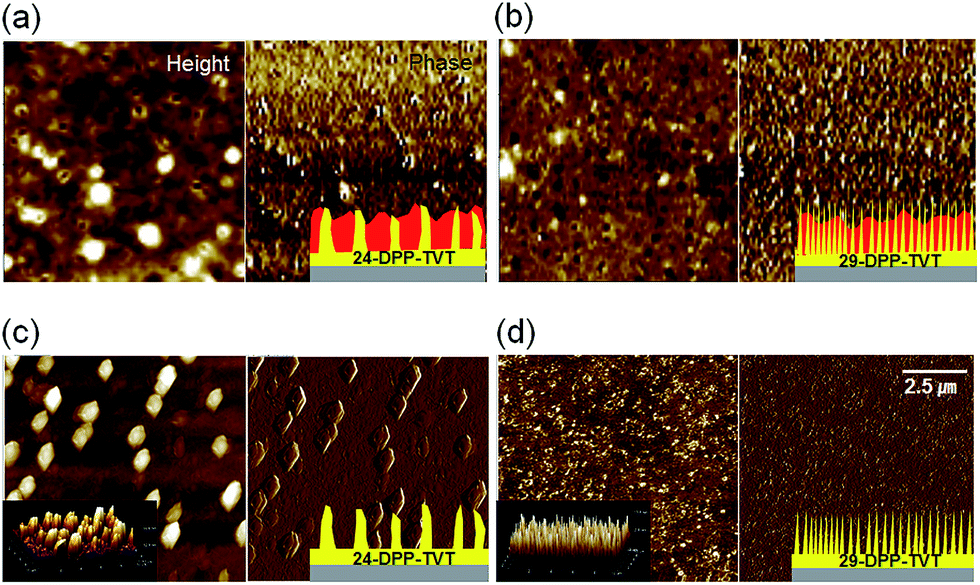 | ||
| Fig. 2 AFM height (left) and phase (right) images of 24-DPP-TVT/PMMA blend film (a), 29-DPP-TVT/PMMA blend film (b), acetic acid-etched 24-DPP-TVT/PMMA blend film (c), acetic acid-etched 29-DPP-TVT/PMMA blend film (d). The insets in the height images show 3D profiles, whereas the insets in the phase images represent the schematic drawings of the obtained structures. | ||
Fig. 3a and c show the 2D-GIXRD patterns of 24-DPP-TVT and 29-DPP-TVT films, respectively. Along out-of-plane directions, (00l) diffraction peaks were predominantly observed in both the patterns. These diffraction patterns correspond to the edge-on lamellar crystalline structures where long alkyl chains are aligned vertical to the substrate surface.3 The 2D-GIXRD patterns of 29-DPP-TVT exhibited more intense diffraction peaks, and angular spreads of these peaks were much narrower compared to those of 24-DPP-TVT. Long alkyl chain spacer increases alkyl chain interaction, thereby promoting lamellar stacking. Fig. 3b and d show the 2D-GIXRD patterns of 24-DPP-TVT/PMMA and 29-DPP-TVT/PMMA blend films, respectively. Because 24-DPP-TVT or 29-DPP-TVT was added as a minor component, intensities of the (001) diffraction peaks decreased. However, crystalline structure of 24-DPP-TVT or 29-DPP-TVT did not change. Notably, broad amorphous halo indicative of PMMA was visible at both the blend films. The angular spreads of the (001) diffraction peaks in 29-DPP-TVT/PMMA were much narrower than those in 24-DPP-TVT/PMMA because of the highly crystalline nature of 29-DPP-TVT with long alkyl chain spacer.
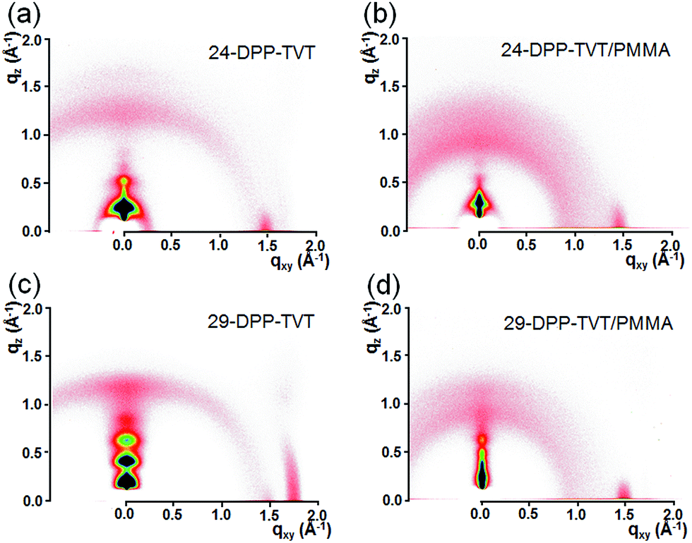 | ||
| Fig. 3 2D-GIXRD patterns of 24-DPP-TVT film (a), 24-DPP-TVT/PMMA blend film (b), 29-DPP-TVT film (c), and 29-DPP-TVT/PMMA blend film (d). | ||
When concentration gradient-induced flow was applied in the transient wetting layer, 24-DPP-TVT or 29-DPP-TVT layer at the bottom moves vertically to the surface.11,16 We speculate that the higher crystallization rate of 29-DPP-TVT in 29-DPP-TVT/PMMA blend accelerates evaporation of solvent, thereby preventing coarsening of the 29-DPP-TVT rods. Thus, spin-cast 29-DPP-TVT/PMMA blend film contains many 29-DPP-TVT rods with small widths. In contrast, the 24-DPP-TVT phase in the 24-DPP-TVT/PMMA blend coarsens during the evaporation of solvent, thereby leading to large phase-separated domains. This phenomenon is typical in polymer/polymer blend when crystallinities of two polymers are low. Fig. S2 in the ESI† show spin-cast P3HT:PMMA (1:3) blend film from chlorobenzene. The AFM images before and after etching PMMA phase indicate laterally phase-separated structure, containing P3HT rods with dimensions of 1–2 μm. These hairy rod structures probably originated from the phase-separation characteristics in polymer blends. When single 24-DPP-TVT or 29-DPP-TVT was spin-casted on the substrate, surface morphology exhibits a featureless image without hairy rods (see Fig. S3 in the ESI†).
Au S/D electrodes were deposited to measure the electrical properties of FETs with 24-DPP-TVT, 29-DPP-TVT and 24-DPP-TVT/PMMA, 29-DPP-TVT/PMMA blend films. Fig. 4a and b show the transfer characteristics of the devices. The field-effect mobilities and on/off current ratios were extracted from the transfer characteristics and are listed in Table 1. 29-DPP-TVT FETs exhibit higher field-effect mobility (0.83 cm2 V−1 s−1) than those of 24-DPP-TVT FETs (0.4 cm2 V−1 s−1), because of increased π–π interaction in longer alkyl chain spacer and corresponds well with previous report.3 When 24-DPP-TVT or 29-DPP-TVT was blended with PMMA, the difference in the electrical properties (24-DPP-TVT/PMMA versus 29-DPP-TVT/PMMA) increased significantly. Field-effect mobility of FETs with 24-DPP-TVT/PMMA blend was calculated to be 0.012 cm2 V−1 s−1, which is over one order of magnitude lower than the value obtained from 24-DPP-TVT FETs. In contrast, 29-DPP-TVT/PMMA blend FETs exhibit an average field-effect mobility of 0.67 cm2 V−1 s−1 and on/off current ratio of 108, which are similar to the values obtained from 29-DPP-TVT FETs. All the devices exhibit similar downward kink behaviors (Fig. 4b). The downward kink, decrease of saturation current at high gate voltage, was commonly observed in recently developed semiconducting polymers containing electron deficient DPP unit.5 Recent report by McCulloch et al. discussed the origins of the downward kink.23 Localized electron trapping near the contact prohibits the use of gradual-channel approximation, thereby misleading extraction of field-effect mobility. We also calculated field-effect mobility at high gate voltage and the extracted mobility values were summarized in Table S1 in ESI.† Although the extracted mobility values at high gate voltage are much lower than the mobility values in Table 1, they share similar trends. To this end, comparative analysis of field-effect mobility is possible notwithstanding inaccuracy in measuring mobility.
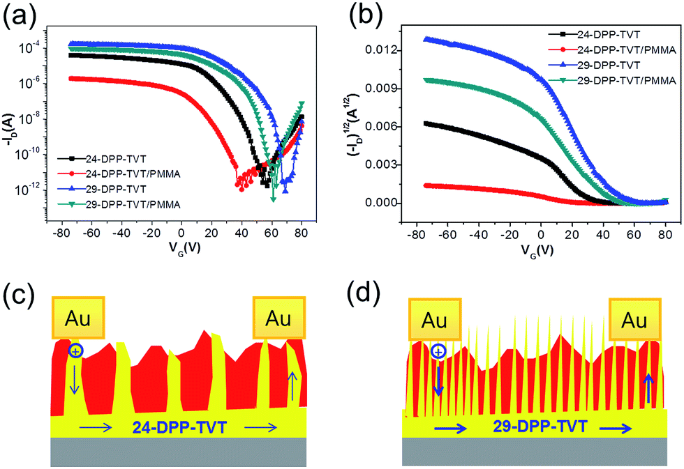 | ||
| Fig. 4 (a) −ID, (b) (−ID)1/2 versus VG characteristics for the FETs based on 24-DPP-TVT film, 24-DPP-TVT/PMMA blend film, 29-DPP-TVT film, and 29-DPP-TVT/PMMA blend film. VD is fixed at −80 V. Schematic drawings of charge injection and transport in the 24-DPP-TVT/PMMA blend film (c), and 29-DPP-TVT/PMMA blend film (d). | ||
| μ [cm2 V−1 s−1] | ION/IOFF | |
|---|---|---|
| DPP-C24 | 0.4 ± 0.09 | 107 |
| DPP-C24/PMMA | 0.012 ± 0.003 | 106 |
| DPP-C29 | 0.83 ± 0.15 | 108 |
| DPP-C29/PMMA | 0.67 ± 0.1 | 108 |
The differences in the electrical properties are related to the differences both in molecular orientation of DPP-based semiconducting polymer and phase-separated structures. 24-DPP-TVT phase in 24-DPP-TVT/PMMA blend exhibits larger angular spread in molecular orientation, thereby leading to low field-effect mobility. This is in stark contrast to 29-DPP-TVT phase in 29-DPP-TVT/PMMA blend, exhibiting smaller angular spread. In addition, 29-DPP-TVT rods in 29-DPP-TVT/PMMA blend provide efficient sites for charge injection, whereas fewer 24-DPP-TVT rods can be obstacle for charge injection from Au electrode to the channel region (Fig. 4c and d). Because thin 24-DPP-TVT layer of 6–7 nm fully covers ODTS modified SiO2/Si substrate, the adverse effects from lateral phase-separation at the channel region can be minimized (see Fig. S1 in the ESI†). Interestingly, DPP-based semiconducting polymer/PMMA FETs exhibit lower turn-on voltages than those of homo DPP-based semiconducting polymer FETs, because of the partial passivation of DPP-based semiconducting polymer by PMMA.22 Because fabrication processes of FETs were conducted under ambient condition, oxygen and water molecules can be permeated into the channel region, thereby leading to the accumulation of hole carriers (positive shift in turn-on voltage). This effect can be reduced in DPP-based semiconducting polymer/PMMA blend film, because PMMA partially passivate DPP-based semiconducting polymer.
4. Conclusions
The effects of crystalline nature in DPP-based semiconducting polymer on the phase-separated structures of DPP-based semiconducting polymer/PMMA blends were investigated. Hierarchical structures containing ultrathin-film (bottom) and hairy rods (top) of DPP-based semiconducting polymers formed on the substrates due to the combined effects of the self-stratification and Marangoni-instability during the phase-separation of polymer blends. In particular, fewer and bigger semiconductor rods were observed in the 24-DPP-TVT/PMMA film, because of coarsening of 24-DPP-TVT phase during solvent evaporation. Highly crystalline nature of 29-DPP-TVT prevented coarsening of the 29-DPP-TVT rods, thereby resulted in densely packed semiconductor rods. The structural characterization revealed that 29-DPP-TVT phase in 29-DPP-TVT/PMMA blend exhibited lower angular spread in molecular orientation compared to 24-DPP-TVT phase in 24-DPP-TVT/PMMA blend. Both the molecular orientation of DPP-based polymer and phase-separated structure of blend film affected the electrical properties of FETs based on DPP-based semiconducting polymer/PMMA blends. Higher field-effect mobility observed in FETs of 29-DPP-TVT/PMMA blend indicates strong dependency of crystalline nature in semiconducting polymer for the use of polymer blends in OFETs. We believe that this study will be useful for selecting suitable semiconducting polymer, which can enhance the electrical properties of OFETs based on dual (vertical/lateral) phase-separation of semiconducting/insulating polymer blends.Acknowledgements
This work was supported by grants from the Basic Science Research Program (Code No. 2016R1C1B2013176) and the Center for Advanced Soft Electronics under the Global Frontier Research Program (Code No. 2011-0031628) of the Ministry of Science, ICT and Future Planning, Korea.References
- Y. N. Li, P. Sonar, L. Murphy and W. Hong, Energy Environ. Sci., 2013, 6, 1684–1710 CAS.
- I. Kang, T. K. An, J. A. Hong, H. J. Yun, R. Kim, D. S. Chung, C. E. Park, Y. H. Kim and S. K. Kwon, Adv. Mater., 2013, 25, 524–528 CrossRef CAS PubMed.
- I. Kang, H. J. Yun, D. S. Chung, S. K. Kwon and Y. H. Kim, J. Am. Chem. Soc., 2013, 135, 14896–14899 CrossRef CAS PubMed.
- Y. Yamashita, F. Hinkel, T. Marszalek, W. Zajaczkowski, W. Pisula, M. Baumgarten, H. Matsui, K. Mullen and J. Takeya, Chem. Mater., 2016, 28, 420–424 CrossRef CAS.
- C. B. Nielsen, M. Turbiez and I. McCulloch, Adv. Mater., 2013, 25, 1859–1880 CrossRef CAS PubMed.
- Y. J. Kwon, Y. D. Park and W. H. Lee, Materials, 2016, 9, 650 CrossRef.
- W. H. Lee and Y. D. Park, Polymers, 2014, 6, 1057–1073 CrossRef.
- S. Goffri, C. Muller, N. Stingelin-Stutzmann, D. W. Breiby, C. P. Radano, J. W. Andreasen, R. Thompson, R. A. J. Janssen, M. M. Nielsen, P. Smith and H. Sirringhaus, Nat. Mater., 2006, 5, 950–956 CrossRef CAS PubMed.
- S. G. Lee, H. S. Lee, S. Lee, C. W. Kim and W. H. Lee, Org. Electron., 2015, 24, 113–119 CrossRef CAS.
- H. M. Kim, H. W. Kang, D. K. Hwang, H. S. Lim, B. K. Ju and J. A. Lim, Adv. Funct. Mater., 2016, 26, 2706–2714 CrossRef CAS.
- D. Kwak, H. H. Choi, B. Kang, D. H. Kim, W. H. Lee and K. Cho, Adv. Funct. Mater., 2016, 26, 3003–3011 CrossRef CAS.
- G. H. Lu, J. Blakesley, S. Himmelberger, P. Pingel, J. Frisch, I. Lieberwirth, I. Salzmann, M. Oehzelt, R. Di Pietro, A. Salleo, N. Koch and D. Neher, Nat. Commun., 2013, 4, 1588 CrossRef PubMed.
- K. Zhao, O. Wodo, D. D. Ren, H. U. Khan, M. R. Niazi, H. L. Hu, M. Abdelsamie, R. P. Li, E. Q. Li, L. Y. Yu, B. Y. Yan, M. M. Payne, J. Smith, J. E. Anthony, T. D. Anthopoulos, S. T. Thoroddsen, B. Ganapathysubramanian and A. Amassian, Adv. Funct. Mater., 2016, 26, 1737–1746 CrossRef CAS.
- L. Qiu, J. A. Lim, X. Wang, W. H. Lee, M. Hwang and K. Cho, Adv. Mater., 2008, 20, 1141–1145 CrossRef CAS.
- W. H. Lee, D. Kwak, J. E. Anthony, H. S. Lee, H. H. Choi, D. H. Kim, S. G. Lee and K. Cho, Adv. Funct. Mater., 2012, 22, 267–281 CrossRef CAS.
- S. Y. Heriot and R. A. L. Jones, Nat. Mater., 2005, 4, 782–786 CrossRef CAS PubMed.
- L. Kergoat, N. Battaglini, L. Miozzo, B. Piro, M.-C. Pham, A. Yassar and G. Horowitz, Org. Electron., 2011, 12, 1253–1257 CrossRef CAS.
- H.-L. Cheng, J.-W. Lin, J. Ruan, C.-H. Lin, F.-C. Wu, W.-Y. Chou, C.-H. Chen, C.-K. Chang and H.-S. Sheu, ACS Appl. Mater. Interfaces, 2015, 7, 16486–16494 CAS.
- R. J. Kline, D. M. DeLongchamp, D. A. Fischer, E. K. Lin, L. J. Richter, M. L. Chabinyc, M. F. Toney, M. Heeney and I. McCulloch, Macromolecules, 2007, 40, 7960–7965 CrossRef CAS.
- J. G. Mei and Z. N. Bao, Chem. Mater., 2014, 26, 604–615 CrossRef CAS.
- S. Jeon, J. H. Lee, I. K. Lee, W. H. Lee and B. G. Kim, Dyes Pigm., 2016, 133, 114–119 CrossRef CAS.
- A. C. Arias, F. Endicott and R. A. Street, Adv. Mater., 2006, 18, 2900 CrossRef CAS.
- I. McCulloch, A. Salleo and M. Chabinyc, Science, 2016, 352, 1521–1522 CrossRef CAS PubMed.
Footnote |
| † Electronic supplementary information (ESI) available. See DOI: 10.1039/c6ra27953h |
| This journal is © The Royal Society of Chemistry 2017 |