
 Open Access Article
 This Open Access Article is licensed under a Creative Commons Attribution-Non Commercial 3.0 Unported Licence
To save half contact pads in 2D mapping of local temperatures with a thermocouple array
Danhong Han ,
Gang Li,
Sikai Zhou,
Zhenhai Wang,
Fan Yang and
Shengyong Xu*
,
Gang Li,
Sikai Zhou,
Zhenhai Wang,
Fan Yang and
Shengyong Xu*
Key Laboratory for the Physics & Chemistry of Nanodevices, Department of Electronics, Peking University, Beijing, 100871, P. R. China. E-mail: xusy@pku.edu.cn
First published on 30th January 2017
Abstract
The rapid development of micro-electronic devices requires smaller sensors with better sensitivity and higher spatial resolution than what could be obtained from sensors currently available. For a two-dimensional (2D) mapping of local temperatures with thin-film thermocouple (TFTC) arrays, a higher spatial resolution usually means a larger amount of sensors in the array, which always leads to more leads and contact pads. We demonstrated here that by using a tree-like array, where all the leads of one material shared a common contact pad, an array consisting of N TFTCs could perform well with only N + 1 contact pads rather than 2N pads for the conventional configuration, resulting in the same 2D maps of local temperature distribution as those measured with a conventional array. The relative error was less than 5%. This simplified device configuration has efficiently reduced the difficulty in wire bonding and device fabrication, therefore it may find applications in novel wearable and flexible devices.
1. Introduction
Along with the development of nanotechnology, wearable devices and the “Internet of Things”, the demand for well-functioning, easy-to-use and widely applicable micro-/nano-scaled temperature sensors has grown rapidly.1–4 Individual thermal sensors and sensor arrays might offer valuable information in the research on nano-electronics and photonic devices,5,6 microfluidics systems7,8 and cell biology at the single-cell level.9–12 As a result, a number of contact methods for temperature sensing at micro-/nano-scales, such as scanning thermal microscopy,13–15 microheaters,16 thin-film thermocouples (TFTC)17,18 and noncontact methods such as thermoreflectance,19 fluorescent thermal imaging11,20,21 and absorption spectroscopy,22 have been developed recently.To increase the spatial resolution in a measuring zone, it is necessary to reduce the size of each sensor and increase the surface density of sensors over the region under test. However, practically it is a technical challenge of spatial arrangement when the number of sensors is continuously increased. For example, for a conventional TFTC array with a 10 × 10 matrix, it needs 200 leads and 200 contact pads. This large amount of pads needs more room on the device and causes unexpected difficulties in wire bonding, interconnection of the device, as well as in the measurement setup for flexible electronics and wearable devices. To solve this problem, Han et al. suggested a smart cross-over configuration, and demonstrated that a diode temperature sensor array (DTSA) with a matrix of 32 × 32 (i.e., 1024) diodes on a 8 mm × 8 mm surface area could perform well only needing 64 leads.23 Such a configuration requires multilayered thin-film fabrication techniques, which require an insulating layer and precise placement of the opening windows for the top layer, and it may not be applicable for TFTC arrays, where the size of each sensor could be as small as 150–500 nm (ref. 24) and the spacing of two neighboring sensors could be smaller than one micron. Liu et al. demonstrated another simplified configuration for TFTC arrays made from one layer of metal film,25 where all the individual TFTCs shared one common thick beam. This elegant structure indeed applied the law of intermediate temperature.26 This law concludes that the voltage output of the testing area depends only on the temperature difference between the junction point and the cold end, regardless of how much the temperature fluctuates between the locations. Unfortunately, the sensitivities of the single-metal TFTCs were all around 1 μV K−1 or less,25,27,28 resulting in a temporal resolution of 0.2–0.5 K. The thick lead is 30 microns in width, thus it may cause more disruption on the thermal flux of the sample surface, which did not meet the requirements of some important applications, e.g., to precisely sense the local temperature distributions of individual live cells.
In this work, we presented a tree-like configuration for TFTC arrays. The device structure is not as simple as the one presented by Han et al. and Liu et al.,23,25 but it reduces almost half of the contact pads while maintaining the same performance as a conventional array does.
2. The design and fabrication
2.1 The structure design
Fig. 1(a) schematically illustrates the structure of a conventional TFTC array made from two materials (film A and film B), where the junctions of the sensors are all located in the testing zone (highlighted with a dashed red oval in the figure) to detect the temperature distribution Th(x,y), where (x, y) are the location coordinates. The contact pads of Ai and Bi (here i = 1, 2, …, 9), also referred as the cold ends, are all located at the cool zone with a constant reference temperature of Tc (highlighted with dashed blue frames). Thus for an array of N sensors, it needs 2N contact pads, and output voltages measured at each pair of contact pads AiBi are taken as the measurement data. Shown in Fig. 1(b), in the tree-like configuration, leads of all Ai are combined into one contact pad A, and later on the voltages measured at ABi are taken as the outputs for the sensor array. | ||
| Fig. 1 Schematic illustration for a conventional TFTC array (a) and a tree-like TFTC array (b). Both TFTC arrays are made from two materials, where their junction areas are highlighted with dashed red ovals. Their cold ends Ai and Bi (i = 1, 2, …, 9 in this figure) are all located at the reference cool zones highlighted with dashed blue frames. For a conventional array with 9 sensors (a), it needs 18 contact pads. For the array with tree-like configuration (b), leads Ai are combined into one contact pad A, thus it only needs 10 contact pads. | ||
We have fabricated a series of testing devices to verify the validity and feasibility of the tree-like TFTC arrays made with Cr and Pd thin films in silicon substrate. Fig. 2 shows one type of our devices. It has a built-in on-site heater at the central region that is made of Pd with 42 TFTCs arranged surround the heater. The area marked by a red circular dashed area in Fig. 2(a) shows the location of the heater and the TFTC sensors. The junctions of the 42 TFTCs are divided into 7 sets, and each set consists of 6 TFTC sensors, located along 7 symmetric lines which point towards the center of the device. However, among the 7 sets of sensors, 4 sets are patterned into the tree-like configuration, and the other 3 sets are made with a conventional configuration for comparison. Fig. 2(b) is an optical micrograph of the central part of the device. It shows clearly the symmetry of pattern made with 42 TFTCs with respect to the central heater. For the 7 lines of TFTC sensors, the first sensor junction of each line has the same distance to the central point of the device, and so are the second, third and sixth sensors in each line. As a result, when an external electric current is applied to the heater, the heater is expected to generate a center-pointed temperature gradient zones with a symmetry close to a circle shape. If all the sensors work with the same sensing performance, their measurement data should show circular isothermal zones. Fig. 2(c) shows details of two sets of 6-TFTC sensors at the left side of the device. At the location about 5.5 mm away from the heater, which is marked with a yellow frame and enlarged in the inset, it shows that the 6 Pd leads merge into one lead. Fig. 2(d) is an optical micrograph of the region marked with a white frame in Fig. 2(c), showing the detailed structure of the Cr/Pd junctions of 6 TFTCs. In the optical microscope, Pd beams appear brighter than Cr beams. The widths of the Pd and Cr beams are kept constant at 10 μm for all the sensors.
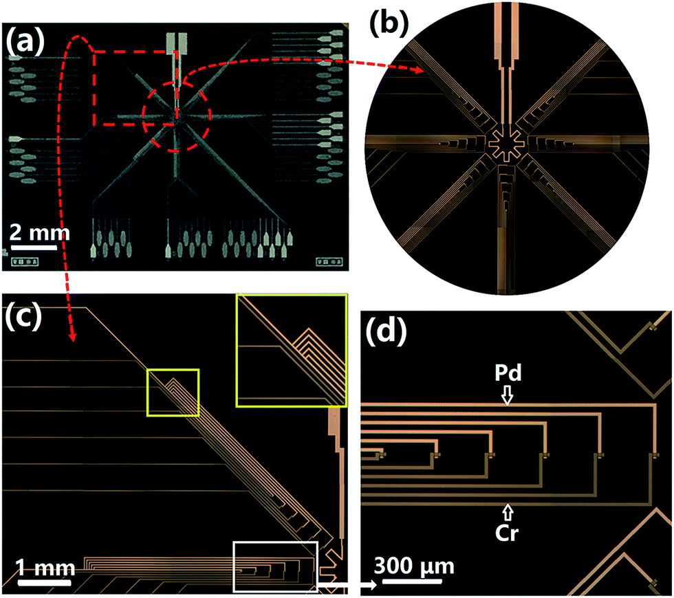 | ||
| Fig. 2 The photo of one type of the tree-like TFTC array. (a) The whole structure is in the photo. It has 6 × 7 TFTCs that are arranged surrounding the heater, 4 sets are patterned into the tree configuration on the left, and the other 3 sets are conventional configuration on the right for comparison. (b) An optical micrograph of the central part of the device. It shows clearly the symmetrical pattern made with 42 TFTCs with respect to the central heater. (c) Shows details of two sets of tree-like TFTC sensors. It shows that the 6 Pd leads merge into one lead at the location about 5.5 mm away from the heater, which is enlarged in the inset. (d) Shows the detailed structure of the Cr/Pd junctions of 6 TFTCs. | ||
2.2 Experimental methods
All the devices described in this work were fabricated with standard cleanroom techniques. The TFTC array patterns were made with a Karl Suss MJB4 mask aligner. Pd thin films were deposited with a Kurt J. Lesker AXXIS e-beam evaporator and Cr thin films were deposited with a Kurt J. Lesker PVD75 magneto-sputtering system. Electrical measurements of the devices were all performed on a homemade platform in the air. The heating power of the on-site heaters was controlled with a Keithley 2400 source-meter. Output voltage signals of the TFTCs were measured with a homemade multiplexer and a Keithley 2182A nanovoltmeter. Real-time two dimensional (2D) mapping of local surface temperatures was recorded with a computerized data acquisition system and calculated with Matlab software.29 The thermopower of the Cr/Pr TFTC sensors was calibrated on a homemade calibration platform, showing a stable average value of 20.87 ± 0.35 μV K−1 for dozens of sensors under test, corresponding to an accuracy of ±0.02 K. The value of thermopower was found not sensitive to the beam width and length of the TFTCs under test.3. Results and discussion
Fig. 3 displays a typical set of measurement results when the device shown in Fig. 2 was tested at the heating power of 190 mW from the central onsite heater. As expected, the pattern of the output voltage distribution, corresponding to the isothermal pattern for temperature increment at the testing zone, is close to symmetric from the left side to the right side. The maximum output voltage is 123.1 μV, corresponding to a temperature increment of 5.9 K. At such a small temperature difference over the test zone, relative large measurement errors could be induced by non-uniformity in material, such as the film thickness and beam width of the Pd and Cr beams, which may change the temperature distribution on the sample surface.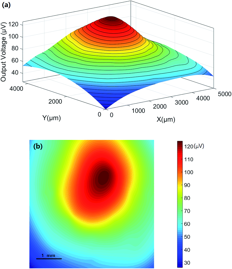 | ||
| Fig. 3 Displays a typical set of 3D (a) and 2D (b) measurement results when the device shown in Fig. 2 was tested at the heating power of 190 mW for the central onsite heater. | ||
We further verified the validity of the tree-like TFTC arrays by testing devices with another configuration. As shown in Fig. 4, two separate devices were fabricated and tested. They have identical parameters for the materials, fabrication processes and patterns. Fig. 4(a) is a device with a tree-like structure, where the central pattern is the same as that shown in Fig. 2. In each of the 7 sensor lines, all the 6 Pd leads merge into one at a distance of 5.5 mm from the central heater. Fig. 4(b) is a device with a conventional structure. It can be seen that, in Fig. 4(a) there are altogether 49 contact pads, while in Fig. 4(b), the device has 84 contact pads.
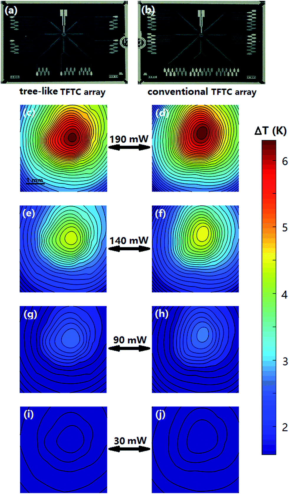 | ||
| Fig. 4 The temperature mapping for the tree-like TFTC array and the conventional TFTC array device in different heating power. (a) and (b) are two optical photographs of the two kinds of finished devices. (c) and (d), (e) and (f), (g) and (h), (i) and (j) represent the measurements for each device at 190 mW, 140 mW, 90 mW, and 30 mW. | ||
In the following figures in the left panel, namely Fig. 4(c), (e), (g) and (i), we can see the 2D mapping of local temperature distributions in the testing zone at heating powers of 30 mW, 90 mW, 140 mW and 190 mW, applied to the onsite heater. The figures of the right panel, namely Fig. 4(d), (f), (h) and (j), show the 2D mapping of local temperature distributions in the testing zone at the same heating powers of 30 mW, 90 mW, 140 mW and 190 mW, respectively. Clearly, each pair of 2D mapping patterns (e.g., Fig. 4(c) and (d)) measured at the same heater power match very well. Careful comparison has been performed between each pair of the patterns and the deviations calculated are listed in Table 1. Average deviations are 2.8%, 3.0%, 3.4%, 3.2%, 4.6%, 4.2% and 3.2% for the heater powers of 190 mW, 140 mW, 90 mW, 50 mW, 30 mW, 15 mW and 5 mW, respectively. That means, the relative difference in the measurement results between those taken from the tree-like TFTC array with 49 contact pads and those from the conventional TFTC array with 84 contact pads is only in the range of 3–5%. In other words, the device with the tree-like array construction functions as well as the conventional array.
| Heating power (mW) | 190 | 140 | 90 | 50 | 30 | 15 | 5 |
| Deviation (%) | 2.8 | 3.0 | 3.4 | 3.2 | 4.6 | 4.2 | 3.2 |
Next we examined the dynamic response of devices with tree-like micro-TFTC arrays. Fig. 5 shows a typical set of the testing results. Fig. 5(a) is a photograph of the measuring setup, where a hot iron was mounted with its tip close to the central point of the device, which has the same pattern as shown in Fig. 4(a). Real-time 2D mapping of the local temperature distribution on the device surface was performed with a technique reported previously.29 Fig. 5(b) is the output voltages across the testing zone at times of 60–140 s after the hot iron was turned on. Corresponding to the location of the yellow dotted line shown in Fig. 5(c). In the following Fig. 5(c)–(k), we plotted the 2D mapping results of the testing zone, corresponding to time points of 60 s, 70 s, 80 s, 90 s, 100 s, 110 s, 120 s, 130 s and 140 s, respectively. They clearly show the increase of central temperature as time goes on. The difference in temperature between the central point and the edge of the testing zone increases from 1.8 K at 60 s to 6.1 K at 140 s. The results show that the device with a tree-like TFTC array has the same dynamic response as that of conventional TFTC arrays as reported previously.
 | ||
| Fig. 5 The dynamic response of devices with tree-like micro-TFTC arrays. (a) A photograph of the measuring setup. (b) The output voltages across the testing zone at set times between 60–140 s after the hot iron is turned on. (c) to (k) We plot the 2D mapping results of the testing zone at the time points of 60 s, 70 s, 80 s, 90 s, 100 s, 110 s, 120 s, 130 s, and 140 s. | ||
In addition to the tree-like TFTC arrays on the silicon substrate, we have fabricated a bunch of new samples, and “printed” the same Pd/Cr TFTC arrays devices on a 75 μm thick PET (polyethylene terephthalate) substrate, by using the same photolithography and thin film deposition techniques described in experimental methods. PET is a substrate that has been extensively applied in flexible electronics.30,31 The pictures of the devices are typically shown in Fig. 6. On one 4-inch substrate, we fabricated 6 different devices and twisted the PET substrate as seen in Fig. 6(a). For instance, the two devices in the middle part are the same as that shown in Fig. 4(a) and (b). The device at the top-right corner in Fig. 6(a) is the same as that shown in Fig. 2, where the central part marked with a red frame is shown in Fig. 6(b), and the part highlighted with a blue frame is shown in Fig. 6(c), it is the area where 6 Pd leads merge into one lead. The optical micrograph shows that all the Pd and Cr beams are clearly patterned with smooth edges.
 | ||
| Fig. 6 Photographs of Pd/Cr TFTC devices fabricated on a PET substrate. (a) Six different devices on one 4-inch PET substrate. (b) The central measurement part of the device at the top-right corner in (a). (c) The area where 6 Pd leads merge into one lead. | ||
4. Conclusion
In summary, we presented a new method for 2D mapping of local temperatures with tree-like TFTC arrays. In a tree-like array, all leads of one type of the two materials are merged into a single common contact pad, therefore it reduces N − 1 contact pads as compared to a conventional TFTC array consisting of N TFTCs. We demonstrated that tree-like micro-TFTC arrays (patterned from Cr/Pd thin films) resulted in the same 2D maps of local temperature distributions as the conventional TFTC arrays did, with a relative error less than 5%. In the dynamic testing, the tree-like TFTC arrays functioned well for real-time 2D mapping in a time scale of 1–10 s, showing an accuracy of ±0.02 K. This technique may be applied in wearable and flexible electronics systems, where saving of contact pads could reduce the difficulty and cost of fabrication processes.Acknowledgements
This work was financially supported by the NSF of China (Grant No. 11374016 and 91221202).References
- D. Langley, G. Giusti, C. Mayousse, C. Celle, D. Bellet and J. P. Simonato, Nanotechnology, 2013, 24, 452001 CrossRef PubMed.
- L. Gao, D. D. Dong, J. G. He, K. K. Qiao, F. R. Cao, M. Li, H. Liu, Y. B. Cheng, J. Tang and H. S. Song, Appl. Phys. Lett., 2014, 105, 4 Search PubMed.
- Z. Q. Zheng, T. M. Zhang, J. D. Yao, Y. Zhang, J. R. Xu and G. W. Yang, Nanotechnology, 2016, 27, 225501 CrossRef PubMed.
- S. S. Won, M. Sheldon, N. Mostovych, J. Kwak, B. S. Chang, C. W. Ahn, A. I. Kingon, I. W. Kim and S. H. Kim, Appl. Phys. Lett., 2015, 107, 5 CrossRef.
- Y.-J. Yu, M. Y. Han, S. P. Berciaud, A. B. Georgescu, T. F. Heinz, L. E. Brus, K. S. Kim and P. Kim, Appl. Phys. Lett., 2011, 99, 183105 CrossRef.
- V. N. Mochalin, O. Shenderova, D. Ho and Y. Gogotsi, Nat. Nanotechnol., 2012, 7, 11–23 CrossRef CAS PubMed.
- R. K. P. Benninger, Y. Koc, O. Hofmann, J. Requejo-Isidro, M. A. A. Neil, P. M. W. French and A. J. deMello, Anal. Chem., 2006, 78, 2272–2278 CrossRef CAS PubMed.
- G. Baffou, R. Quidant and F. J. G. de Abajo, ACS Nano, 2010, 4, 709–716 CrossRef CAS PubMed.
- D. Jaque, B. del Rosal, E. M. Rodriguez, L. M. Maestro, P. Haro-Gonzalez and J. G. Sole, Nanomedicine, 2014, 9, 1047–1062 CrossRef CAS PubMed.
- G. Kucsko, P. C. Maurer, N. Y. Yao, M. Kubo, H. J. Noh, P. K. Lo, H. Park and M. D. Lukin, Nature, 2013, 500, 54–58 CrossRef CAS PubMed.
- J. S. Donner, S. A. Thompson, M. P. Kreuzer, G. Baffou and R. Quidant, Nano Lett., 2012, 12, 2107–2111 CrossRef CAS PubMed.
- C. Gota, K. Okabe, T. Funatsu, Y. Harada and S. Uchiyama, J. Am. Chem. Soc., 2009, 131, 2766–2767 CrossRef CAS PubMed.
- S. Gomès, A. Assy and P.-O. Chapuis, Phys. Status Solidi A, 2015, 212, 477–494 CrossRef.
- S. Sadat, A. Tan, Y. J. Chua and P. Reddy, Nano Lett., 2010, 10, 2613–2617 CrossRef CAS PubMed.
- Y. Zhang, C. L. Hapenciuc, E. E. Castillo, T. Borca-Tasciuc, R. J. Mehta, C. Karthik and G. Ramanath, Appl. Phys. Lett., 2010, 96, 062107 CrossRef.
- J.-W. Han and M. Meyyappan, IEEE Sens. J., 2016, 16, 5543–5547 CrossRef.
- C. F. Fang, D. Lee, B. Stober, G. G. Fuller and A. Q. Shen, RSC Adv., 2015, 5, 85620–85629 RSC.
- F. L. Bakker, J. Flipse and B. J. van Wees, J. Appl. Phys., 2012, 111, 084306 CrossRef.
- Y. S. Ju and K. E. Goodson, J. Heat Transfer, 1998, 120, 306–313 CrossRef CAS.
- Z. Wang, D. Ananias, A. Carné-Sánchez, C. D. S. Brites, I. Imaz, D. Maspoch, J. Rocha and L. D. Carlos, Adv. Funct. Mater., 2015, 25, 2824–2830 CrossRef CAS.
- K. Okabe, N. Inada, C. Gota, Y. Harada, T. Funatsu and S. Uchiyama, Nat. Commun., 2012, 3, 705 CrossRef PubMed.
- G. Casa, A. Castrillo, G. Galzerano, R. Wehr, A. Merlone, D. Di Serafino, P. Laporta and L. Gianfrani, Phys. Rev. Lett., 2008, 100, 200801 CrossRef CAS PubMed.
- I. Y. Han and S. J. Kim, Sens. Actuators, A, 2008, 141, 52–58 CrossRef CAS.
- X. Huo, Z. Wang, M. Fu, J. Xia and S. Xu, RSC Adv., 2016, 6, 40185–40191 RSC.
- H. Liu, W. Sun and S. Xu, Adv. Mater., 2012, 24, 3275–3279 CrossRef CAS PubMed.
- D. Finch, Its Measurement and Control in Science and Industry, 1962, Part2, p. 3 Search PubMed.
- X. Huo, H. Liu, Y. Liang, M. Fu, W. Sun, Q. Chen and S. Xu, Small, 2014, 10, 3869–3875 CrossRef CAS PubMed.
- X. Huo, J. Xu, Z. Wang, F. Yang and S. Xu, Nanoscale Res. Lett., 2016, 11, 351 CrossRef PubMed.
- G. Li, Z. Wang, X. Mao, Y. Zhang, X. Huo, H. Liu and S. Xu, Sensors, 2016, 16, 977 CrossRef PubMed.
- K. J. Yu, D. Kuzum, S. W. Hwang, B. H. Kim, H. Juul, N. H. Kim, S. M. Won, K. Chiang, M. Trumpis, A. G. Richardson, H. Cheng, H. Fang, M. Thompson, H. Bink, D. Talos, K. J. Seo, H. N. Lee, S. K. Kang, J. H. Kim, J. Y. Lee, Y. Huang, F. E. Jensen, M. A. Dichter, T. H. Lucas, J. Viventi, B. Litt and J. A. Rogers, Nat. Mater., 2016, 15, 782–791 CrossRef CAS PubMed.
- D.-H. Kim, N. Lu, R. Ma, Y.-S. Kim, R.-H. Kim, S. Wang, J. Wu, S. M. Won, H. Tao, A. Islam, K. J. Yu, T.-i. Kim, R. Chowdhury, M. Ying, L. Xu, M. Li, H.-J. Chung, H. Keum, M. McCormick, P. Liu, Y.-W. Zhang, F. G. Omenetto, Y. Huang, T. Coleman and J. A. Rogers, Science, 2011, 333, 838–843 CrossRef CAS PubMed.
| This journal is © The Royal Society of Chemistry 2017 |