
 Open Access Article
 This Open Access Article is licensed under a
 Creative Commons Attribution 3.0 Unported Licence
Transparent conducting oxide thin films of Si-doped ZnO prepared by aerosol assisted CVD
Dominic B. Potter ,
Michael J. Powell,
Jawwad A. Darr,
Ivan P. Parkin and
Claire J. Carmalt*
,
Michael J. Powell,
Jawwad A. Darr,
Ivan P. Parkin and
Claire J. Carmalt*
Department of Chemistry, University College London, 20 Gordon Street, London, WC1H 0AJ, UK. E-mail: c.j.carmalt@ucl.ac.uk
First published on 9th February 2017
Abstract
For the first time, aerosol assisted chemical vapour deposition (AACVD) was used to deposit Si-doped ZnO thin films on glass. Depositions were done at a temperature of 450 °C. The precursor solution was made by dissolving the air-stable compounds zinc acetylacetonate and tetraethyl orthosilicate in methanol with a small addition of acetic acid to aid solubility. The dopant concentration in the precursor solution was optimised to find the best optoelectronic properties. The incorporation of Si into the ZnO lattice was confirmed by unit cell volumes calculated from X-ray diffraction (XRD) data and by X-ray photoelectron spectroscopy (XPS). The films consisted of pure phase wurtzite ZnO, with preferred orientation in the (002) plane. Scanning electron microscopy (SEM) was used to examine the surface morphology of the films. The optical properties of the films were analysed using UV/vis spectroscopy and indicated that the average transmittance in the visible part of the spectrum (400–700 nm) varied between 72% and 80%. The electrical properties of the films were obtained from Hall effect measurements using the van der Pauw method. The incorporation of Si into the films resulted in a decrease in resistivity down to a minimum value of 2.0 × 10⁻² Ω cm for the film deposited from a 4 mol% Si![[thin space (1/6-em)]](https://www.rsc.org/images/entities/char_2009.gif) :Zn ratio in the precursor solution. This conductive film was a significant improvement over the non-conductive undoped ZnO film.
:Zn ratio in the precursor solution. This conductive film was a significant improvement over the non-conductive undoped ZnO film.
Introduction
Transparent conducting oxides (TCOs) are an important class of semiconductor material that combine the properties of low electrical resistivity (<10−3 Ω cm) and high optical transmittance (>80%) in the visible region. These desirable characteristics have led to the employment of TCO materials in several optoelectronic applications, including solar panels, liquid crystal displays (LCDs), and light emitting diodes (LEDs).1,2TCO thin films have been prepared via magnetron sputtering, pulsed laser deposition (PLD), atomic layer deposition (ALD), spray pyrolysis, sol–gel deposition, and chemical vapour deposition (CVD).3–10 Atmospheric pressure chemical vapour deposition (APCVD) is regularly used for industrial depositions. This technique involves the vaporisation of volatile precursors within a bubbler, before transporting them to a heated substrate via a carrier gas.
A useful variation of APCVD is aerosol assisted chemical vapour deposition (AACVD). With AACVD, rather than vaporising volatile precursors, soluble precursors are dissolved in a suitable solvent. An aerosol ‘mist’ is then generated from the solvent, usually with a piezoelectric humidifier. The mist is then carried to the heated substrate, where the solvent evaporates away, leaving gaseous precursor compounds. A deposition similar to APCVD can then occur – typically via nucleation of precursors on the substrate surface, followed by surface reaction, and then film growth.
AACVD has several important advantages over APCVD. APCVD relies on the use of volatile precursors, whilst AACVD relies on the use of soluble precursors. Thus, if there are no appropriate precursors available for APCVD, a CVD-type deposition can still be performed via AACVD, using alternative precursors. Additionally, by varying the solvent used to make up the precursor solution, the morphology can be controlled, which can in turn drastically alter the film properties such as conductivity.11 Furthermore, AACVD is relatively inexpensive, as it simplifies the precursor vapour generation and delivery process in comparison to APCVD. In APCVD, the bubbler and the piping leading to the reaction chamber must all be heated to prevent condensation of the vaporised precursors before they reach the substrate. In AACVD, only the substrate needs to be heated. AACVD can also be conducted in an open atmosphere, and thus it does not require a complicated reactor system.11–13
Indium tin oxide (ITO) and fluorine tin oxide (FTO) are currently the most commonly used TCO materials in industry.10,14,15 However, as a result of the increasing scarcity of indium and tin, and the present high cost, alternative, more sustainable materials for TCO applications are highly sought after. Doped ZnO materials have been widely investigated for TCO applications, due to their wide direct band gap and low resistivity.16–19 Additionally, there are many relatively inexpensive Zn precursors available, due to the higher natural abundance of Zn compared to both In and Sn.20 Therefore, ZnO-based TCO materials can usually be deposited inexpensively.
The main dopants for ZnO are the group 13 elements – Al, Ga, and In.21 These dopants have been used by many groups to consistently prepare highly conductive, high-quality n-type ZnO films.17 Minami et al. established Si as a dopant for ZnO, as it was suggested that Si doping would have a less detrimental effect on the amorphous silica layer found in solar cells.22 Furthermore, Si is inexpensive in comparison to both Ga and In. Computational studies have shown that Si will substitute for Zn in the ZnO lattice due to the low defect formation energy.23 An advantage of using Si as a dopant is that it can act as a multielectron donor. This is beneficial because each dopant ion that is incorporated into a crystal acts as a scattering centre, so multielectron donors can provide higher charge carrier concentrations, whilst keeping the scattering centres to a minimum, thus leading to high conductivity.24 Si-doped ZnO (SZO) thin films have been deposited previously by various techniques, including spray pyrolysis,25 pulsed laser deposition (PLD),26 direct current (DC) magnetron sputtering,27 and atomic layer deposition (ALD).7
In this work, SZO thin films were deposited on glass substrates via AACVD for the first time. The electrical properties of the films were greatly enhanced in comparison to undoped ZnO deposited in the same conditions.
Experimental
Film synthesis
AACVD depositions were carried out as detailed in previous work.28 All chemicals were used as bought: zinc acetylacetonate (Zn(acac)2) (Sigma Aldrich, Dorset, UK), tetraethyl orthosilicate (TEOS) (98%, Sigma Aldrich, Dorset, UK), acetic acid (99%, Fisher, Leicestershire, UK), methanol (99.9%, Fisher, Leicestershire, UK) and nitrogen gas (99.99%, BOC, Surrey, UK).A typical precursor solution was made by dissolving Zn(acac)2 (0.50 g, 1.90 mmol) in methanol (20 mL), and then adding a dopant quantity of TEOS. Acetic acid (∼1 mL) was added to improve the solubility of the Zn(acac)2. The solution was stirred for at least 10 minutes in a bubbler. The substrate was a 3.2 mm thick float glass plate (Pilkington Technology Management Limited, Lancashire, UK), precoated with a 50 nm thick SiO2 barrier layer to prevent leeching of ions between the substrate and the film. The glass was cut to an area of 15 cm × 4 cm, and was then washed using soapy water, acetone and isopropanol. The substrate was then laid horizontally on a carbon heating block, and heated in a quartz tube to 450 °C, with a top plate suspended approximately 8 mm above, parallel to the substrate, to ensure laminar flow of the aerosol. An aerosol mist of the precursor solution was generated using a ‘Liquifog’ piezo ultrasonic atomizer from Johnson Matthey, which uses an operating frequency of 1.6 MHz to produce a mode droplet size of 3 μm. Nitrogen gas was used as a carrier gas to transport the aerosol to the heated substrate, at a rate of 1 L min−1. The reactor exhaust was vented into a fume cupboard. When the precursor solution and associated aerosol mist had been completely emptied from the bubbler, the coated substrate was cooled under a continuous flow of N2 gas, until the temperature was below 100 °C before it was removed from the reactor.
Film characterisation
X-ray diffraction (XRD) patterns were recorded using a Bruker D8 Discover X-ray diffractometer using monochromatic Cu Kα1 and Kα2 radiation of wavelengths 1.54056 and 1.54439 Å respectively, emitted in an intensity ratio of 2:1 with a voltage of 40 kV and a current of 40 mA. The incident beam angle was in a grazing setup at 1° and data was collected between 10° and 66° 2θ with a step size of 0.05° at 2 s per step. Lattice parameters were calculated from the XRD data using GSAS and EXPGUI software.29,30 X-ray photoelectron spectroscopy (XPS) was done using a Thermo Scientific K-alpha spectrometer with monochromated Kα radiation, a dual beam charge compensation system and constant pass energy of 50 eV, with a spot size of 400 μm. Data was fitted using CasaXPS software. Scanning electron microscope (SEM) images were obtained using a JEOL JSM-6301F SEM at an acceleration voltage of 5 kV. UV/vis spectrometry was done using a Perkin Elmer Lambda 950 UV/Vis/NIR Spectrophotometer in both transmission and in diffuse reflectance mode. Room temperature Hall effect measurements were carried out on an Ecopia HMS-3000, which utilises the van der Pauw method. Measurements were taken using a 0.58 T permanent magnet and a current of 1 μA.
Results and discussion
Film synthesis
SZO thin films were successfully deposited on glass substrates via AACVD. Zn(acac)2 and TEOS were used as the Zn precursor and the Si precursor respectively. Zn(acac)2 can be purchased at a lower cost than several other commonly used Zn precursor compounds, including diethyl zinc,31–33 zinc acetate,34–36 and Zn(thd)2 (thd = 2,2,6,6-tetramethyl-3,5-heptadionate).21 Furthermore, diethyl zinc, which is perhaps the most commonly used Zn precursor, is highly pyrophoric, which makes its use hazardous and non-trivial. As Zn(acac)2 is an air stable solid compound, it is very safe and easy to handle, which makes it attractive for use in industry.Rashidi et al. deposited SZO films via the related spray pyrolysis technique, however the solvent used was a mixture of water and isopropanol.25 In this work, methanol was used, which is a more reducing solvent and hence should promote oxygen vacancies.
The methanol solution was carried to the substrates using N2 carrier gas. Depositions were performed at 450 °C and took ca. 40 minutes. The ease of synthesis is an important factor when considering the merits of the films, as they were deposited in an open atmosphere, from an inexpensive, air-stable solution. The resultant films were highly stable, were adherent to the glass substrates, and appeared optically transparent (≥72%).
As the 6 mol% SZO film displayed the highest transparency value of 80% as well as good electrical properties (Table 1), this deposition was repeated at 500 °C and 550 °C to investigate whether a higher deposition temperature would improve the film properties. It was observed that with increasing deposition temperature, the films appeared visibly darker, which was most likely due to an increase in the amount of carbon being incorporated into the films. Additionally, the electrical properties diminished significantly; the films deposited at higher temperature were too resistive to give any Hall values using the van der Pauw technique. Due to the considerable reduction in optoelectronic properties, these films were not selected for further analysis, and thus will not be included in the remainder of this section.
| % Si | V/Å−3 | Tλ400–700/% | Eg/eV | ρ/×10−2 Ω cm | RSh/Ω□−1 | n/×1019 cm−3 | μ/cm2 V−1 s−1 |
|---|---|---|---|---|---|---|---|
| 0.0 | 47.878 (7) | 74 | 3.16 | N/A | N/A | N/A | N/A |
| 0.2 | 47.643 (4) | 75 | 3.19 | 24.0 | 2400 | 0.44 | 5.9 |
| 0.5 | 47.638 (3) | 72 | 3.18 | 11.7 | 1170 | 1.14 | 4.7 |
| 2.0 | 47.617 (5) | 73 | 3.19 | 2.1 | 212 | 2.49 | 11.9 |
| 4.0 | 47.610 (1) | 75 | 3.19 | 2.0 | 201 | 2.64 | 16.5 |
| 6.0 | 47.595 (6) | 80 | 3.20 | 2.5 | 254 | 1.63 | 15.1 |
| 8.0 | 47.59 (2) | 76 | 3.18 | 8.1 | 809 | 1.02 | 7.6 |
| 10.0 | 47.56 (2) | 77 | 3.09 | N/A | N/A | N/A | N/A |
Crystal structure
The crystal structure of the films was determined using X-ray diffraction (XRD), as shown in Fig. 1a. All of the as-prepared films consisted of pure-phase wurtzite ZnO. Due to the nature of thin films, strain is often experienced during growth, which leads to preferred orientation of certain crystal planes. For these films, the preferred orientation was in the (002) direction, perpendicular to the surface of the substrate. This c-axis orientation has been observed previously in SZO thin films deposited by various techniques.7,25–27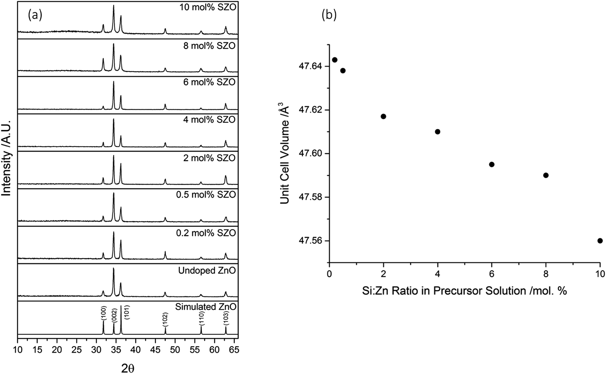 | ||
| Fig. 1 (a) XRD patterns of simulated bulk wurtzite ZnO (ICSD #82028), as well as undoped, and Si-doped ZnO films deposited via AACVD. The apparent rise of an amorphous feature in the 10% SZO film is simply because the peak intensities for that diffraction pattern were lower, resulting in a slight “stretching” of the image, relative to the other diffraction patterns. (b) The trend shown in the unit cell volumes of the SZO films upon increasing Si concentration in the precursor solution. | ||
In order to extract the unit cell volumes of the films, LeBail refinement was performed on the diffraction patterns using GSAS and EXPGUI.29,30 It was observed that the unit cell volumes decreased linearly as the Si concentration was increased in the precursor solution (Fig. 1b). This can be attributed to the smaller ionic radius of Si4+ (0.4 Å) in comparison to Zn2+ (0.74 Å).7,37 It has been suggested through computational studies that Sis(Zn) has a lower formation energy than Sis(O), Sii(tet), or Sii(oct).23,24 With increasing Si concentration, there will be an increase in the substitution of Zn2+ for the smaller Si4+. This will result in a reduction in the size of the unit cell. The observation of a decrease in unit cell volume with increasing Si concentration implies that the Si had been successfully incorporated into the ZnO lattice. The linear reduction in unit cell volume suggests that the amount of Si incorporated into the ZnO lattice was strongly dependant on the initial amount of Si used in the precursor solution.
Elemental analysis
The elemental concentrations were obtained using X-ray photoelectron spectroscopy (XPS). The concentrations were obtained both at the film surfaces, and within the bulk of the films after etching. XPS analysis confirmed the presence of Zn in each sample, with a binding energy of 1022.5 eV for the Zn 2p3/2 peak, which closely matches literature values of ZnO (±0.4 eV).38,39 Incorporation of Si into the ZnO structure was also confirmed, with the Si 2p3/2 peaks generally being centred around 102.2 eV. This is within 1.0–1.5 eV of literature values of pure SiO2.40–42 The larger discrepancy of the Si 2p binding energies in comparison to the values measured for the Zn 2p could be due to the delocalisation of the Si4+ electrons into the ZnO structure, resulting in a lower binding energy.The concentration of Si in the film, both at the surface and in the bulk, increased as the amount of Si used for the precursor solution was increased. Again, this suggests that the amount of Si incorporated into the ZnO lattice was strongly dependant on the initial amount of Si used in the precursor solution (Fig. 2).
 | ||
| Fig. 2 Si:Zn ratios at the surfaces and within the bulks of the films, as determined by XPS. Despite the gradual increase at both the surface and the within the bulk of the films, the amount of Si increases more rapidly at the surface, indicating a competing, secondary Si phase formation. | ||
Comparison of the Si concentration obtained at the surface and the concentration after etching indicate that there has been a significant segregation of the dopant towards the uppermost few nanometres of the film (Fig. 3). This is likely due to the competing reaction of the formation of a thin surface layer of SiO2, which would be amorphous as it was not observed by XRD. This non-conductive surface oxide layer could also explain why the resistivity values of the films aren't as low as SZO films prepared by other methods,16 however the ease of preparation makes AACVD a scalable technique. This was analogous to Al-doped ZnO thin films prepared previously via AACVD, which also used methanol solutions containing Zn(acac)2 as the Zn precursor.28
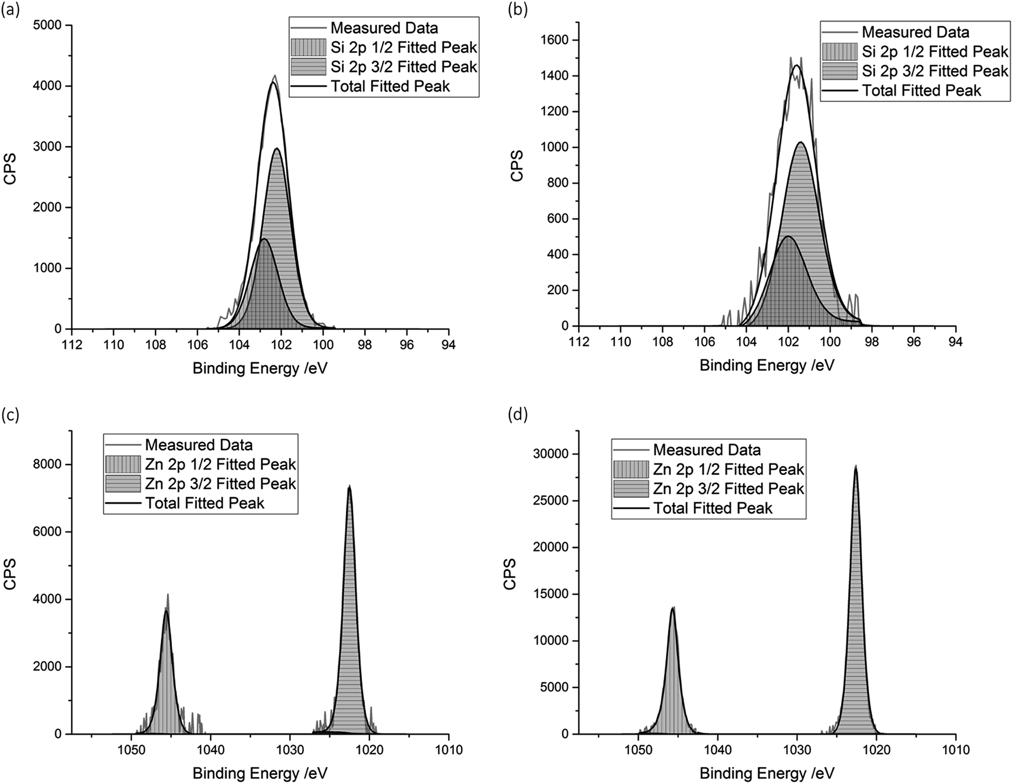 | ||
| Fig. 3 XPS spectra for the 10 mol% SZO film, showing the (a) Si 2p signal measured at the surface, (b) Si 2p signal measured after etching, (c) Zn 2p signal measured at the surface, and (d) Zn 2p signal after etching. | ||
Surface morphology
The surface morphologies of the films were analysed using scanning electron microscopy (SEM). The morphologies were fairly consistent, with the films displaying a grain structure consisting of well-defined, layered, plate-like structures. These grains appeared to be hexagonal in shape and were approximately 1–2 μm in diameter (Fig. 4).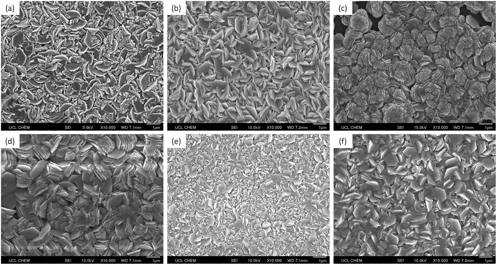 | ||
| Fig. 4 SEM images of (a) undoped ZnO, (b) 0.5 mol% Si-doped ZnO, (c) 4 mol% Si-doped ZnO, (d) 6 mol% Si-doped ZnO, (e) 8 mol% Si-doped ZnO, and (f) 10 mol% Si-doped ZnO. | ||
From the SEM images of the 6 mol% Si-doped ZnO film, new hexagonal layers can be seen growing from the centres of the surfaces of the hexagonal grains, indicating the layer-by-layer growth mechanism of the grains (Fig. 5a). This layered hexagonal grain structure is similar to SZO films deposited by spray pyrolysis at 450 °C by Rashidi et al., however the grains therein were approximately 10 times smaller, at ca. 200 nm in diameter.25 This may be due to the shorter residence time that the precursor solution experiences in a spray pyrolysis deposition, as the solution is sprayed directly at the heated substrate. In AACVD, the aerosol mist is carried more gently over the heated substrate, which can allow for more time for molecular mixing and for grain growth. This is significant, as a larger grain size is often desired for TCOs, due to the reduction in grain boundary scattering, and hence the increase in carrier mobility.43
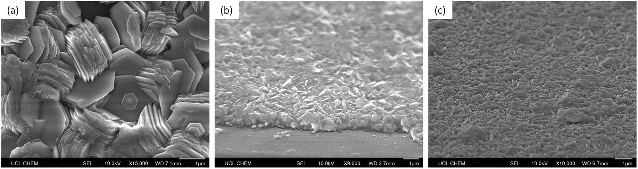 | ||
| Fig. 5 SEM images of (a) 6 mol% Si-doped ZnO, showing the layered growth mechanism of the hexagonal grains, (b) angled view of the edge of the 8 mol% Si-doped ZnO film, showing the typical 1 μm film thickness, and (c) angled view of the 10 mol% Si-doped film, showing a typical surface morphology. | ||
The film thicknesses were determined using side-on SEM, and consistently shown to be 1 μm (Fig. 5b), thus indicating a growth rate of approximately 1.5 μm per hour. The consistent morphologies and film thicknesses indicate that the inclusion of Si in the precursor solution did not affect the solubility of Zn ions in the solution, nor did it hinder the delivery of the aerosol to the substrate.
The highly textured surface morphologies could be advantageous for applications such as solar cells, in which a rough surface morphology is desired in order to promote the scattering light and minimise losses through reflection.10,44,45
Optical properties
The optical properties of the films were analysed using UV/vis spectroscopy. The average transmittance across the visible part of the spectrum (400–700 nm) fluctuated between 72–80%, although it generally increased with Si concentration (Table 1). The film with the highest transmittance was the 6 mol% SZO film, which displayed an average transmittance of 80% across the visible part of the spectrum. This is significant, as it achieved the industrial requirement of 80% transmittance across the visible part of the spectrum.10,31 The undoped film achieved an average transmittance of 74% across the visible part of the spectrum. This is notably higher than the undoped ZnO film deposited by spray pyrolysis by Rashidi et al., which displays a relatively low transmittance across the visible range of approximately 50–60%, possibly indicating high amounts of carbon contamination.25The UV/vis spectra for the films with different Si concentrations were fairly consistent across the range of wavelengths that were scanned. None of the spectra showed a significant decrease of transmission at longer wavelengths, nor a significant increase of reflectance at longer wavelength; rather, the transmission spectra and the reflectance spectra only fluctuated within an approximate range of ±10% and ±4% respectively across the entire infrared region that was measured (Fig. 6). This indicates that these SZO films would not be appropriate for low-emissivity coatings, which require a high reflectance in the IR range.10,32,46
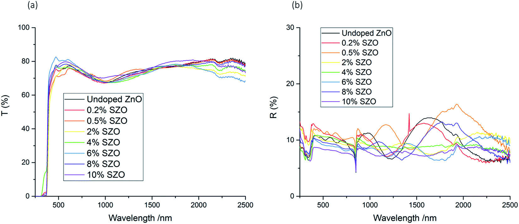 | ||
| Fig. 6 UV/vis spectra showing the (a) transmission, and (b) reflectance of the films. | ||
Tauc plots were used to extract the band gaps from the transmission-reflection spectra (Fig. 7). The band gap increased from 3.16 eV for the undoped ZnO film to between 3.18 and 3.20 eV for the SZO films (up to 8% Si). The observed band gap widening is due to the Burstein–Moss effect, whereby electrons provided by the Si occupy the conduction band, thus raising the Fermi level, EF.8,47–49 Hence, Si doping was a good route to improve the electrical properties of ZnO thin films, whilst maintaining high visible light transmission. The exception to this was the 10 mol% SZO film, in which the band gap dropped to 3.09 eV. This could be due to the band gap narrowing effect, which is a result of many-body interactions involving charge carriers and impurities.26,49,50
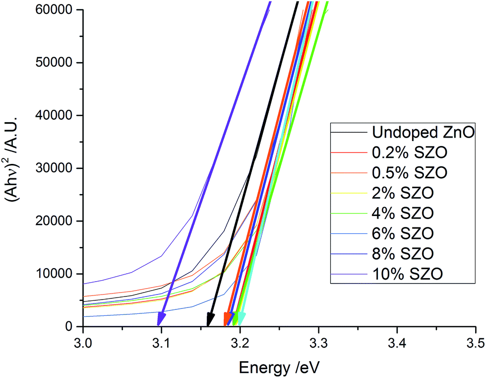 | ||
| Fig. 7 Tauc plots of the as-deposited films. The initial increase and eventual decrease in the band gaps is apparent. | ||
The exponential decay of the Tauc plot at lower energy values is known as the Urbach tail. It is commonly associated with disorder within the material, such as poor crystallinity, or defects such as dopants.51–53 The imperfect crystallinity of the films has resulted in an Urbach tails in the Tauc plots, however they do not follow a significant trend.
Electrical properties
The resistivity, bulk carrier concentration, and electron mobility of the films were obtained using the van der Pauw method. Both the undoped ZnO film and the 10 mol% SZO film were too resistive to give any values using this technique. The incorporation of Si into ZnO resulted in an initial decrease in resistivity down to 2.0 × 10⁻² Ω cm for 4 mol% Si, as well as an increase in charge carrier concentration up to −2.64 × 1019 cm3 and an increase in electron mobility up to 16.5 cm2 V−1 s−1. This mobility value is higher than several Al-doped ZnO thin films deposited by a variety of methods.6,8,28,54,55 Additionally, it approaches the mobility values of common fluorine-doped tin oxide (FTO) industrial coatings, such as TEC™15, which has an electron mobility of 21 cm2 V−1 s−1.56The Hall effect measurements also indicated that the films are all n-type semiconductors, with electrons as the majority charge carriers.
The improved electrical properties in comparison to undoped ZnO show that the Si was successfully acting as an electron donor, providing electron density into the conduction band, and thus increasing the conductivity of the films. At Si concentrations >4%, however, the electrical properties began to diminish again. For comparison, Rashidi et al. observed an increase in resistivity at >3% Si concentration for their films deposited by spray pyrolysis, which is consistent with the observations in this work.25
As the surface morphology remained consistent at higher dopant concentration, the variation in electrical properties cannot be attributed to the grain structure. This is significant, as a reduction in grain diameter will generally result in increased grain boundary scattering, hence reducing carrier mobility.3,57,58 The increase in resistivity is more likely to be attributed to the high levels of dopant incorporation, which can often lead to a reduction in electrical properties. This could, for instance, be due to ionized impurity scattering. This scattering process is thought to determine the transport for conductive materials with a charge carrier concentration greater than 1019 cm−3.59 Additionally, at higher levels of dopant concentration, there is a higher probability of forming various Si–O bonds at the grain boundaries, which will inhibit the transport of electrons.26 Furthermore, the segregation of Si towards the surface of the films, as indicated by XPS, could be the result of a non-conducting SiO2 layer, which would also diminish the electrical properties of the films at high dopant concentration.
Computational studies have shown that Si dopant ions are more likely to form Sis(Zn) defects, as there is a smaller defect formation energy in comparison to Sis(O), Sii(tet), or Sii(oct).23,24 However, at higher dopant concentrations, the solubility limit for dopant incorporation at substitutional sites will be reached, resulting in further impurities occupying interstitial sites and forming secondary phases (e.g. oxides at grain boundaries, or at the surface).60 Interstitial defects act as scattering centres which reduce the carrier mobility, hence the decrease in carrier mobility observed at higher dopant concentration.
In the case of interstitial Si, the donor states that form are too deep in the band gap to contribute any significant electron density to the conduction band.60,61 Similarly, the Si that forms oxide bonds remains electrically inactive and does not donate electrons to the conduction band.26 Therefore, at higher dopant concentrations, the charge carrier concentration has a tendency to saturate or even decrease.26,60
Despite the loss of conductivity at higher dopant concentrations, the improvement in electrical properties in comparison to the undoped ZnO film deposited using the same conditions is evident, and therefore Si is an effective, inexpensive dopant to improve the electrical properties of ZnO films deposited via AACVD.
Further improvements in conductivity could potentially be achieved by co-doping Si with F. An analogous improvement has been observed by Ponja et al., who deposited Al-doped ZnO films via AACVD.62 Co-doping Al with F resulted in enhanced electronic properties in comparison to doping just with Al. Thus, this could be a route to improving film conductivity.
Conclusions
For the first time, Si-doped ZnO thin films were deposited on glass via AACVD, using inexpensive and stable precursors. The Si was successfully incorporated into the ZnO to give a pure wurtzite crystal structure. The amount of Si incorporated into the film was strongly dependant on the initial concentration in the precursor solution. The unit cell volume diminished linearly with increasing dopant concentration. The resultant film morphologies were fairly consistent, comprising hexagonal grains which were approximately 1–2 μm in diameter. The incorporation of Si4+ ions resulted in an initial improvement in electrical resistivity, reaching a minimum value of 2.0 × 10⁻² Ω cm for 4 mol% Si, before increasing again at higher dopant concentration, most likely due to scattering effects as a result of interstitial Si, and various Si–O bonds at grain boundaries and at the film surface.This work has shown that the optoelectronic properties of pure ZnO thin films deposited by AACVD can be improved dramatically by doping with Si. It has also demonstrated the reliability of the AACVD method, which is a scalable technique that allows high quality thin films to be deposited at low cost, and with ease.
Acknowledgements
The authors would like to thank the EPSRC for grant EP/L017709 and UCL for an impact studentship (D. B. P.), as well as NSG (Pilkington Technology Management Limited, European Technical Centre, Hall Lane, Lathom, Nr. Ormskirk, L40 5UF, UK) for their support.References
- D. S. Ginley and C. Bright, MRS Bull., 2000, 15–18 CrossRef CAS.
- H. Liu, V. Avrutin, N. Izyumskaya, Ü. Özgr and H. Morkoç, Superlattices Microstruct., 2010, 48, 458–484 CrossRef CAS.
- S. Calnan and A. N. Tiwari, Thin Solid Films, 2010, 518, 1839–1849 CrossRef CAS.
- K. L. Chopra, S. Major and D. K. Pandya, Thin Solid Films, 1983, 102, 1–46 CrossRef CAS.
- K. Ellmer, J. Phys. D: Appl. Phys., 2000, 33, R17–R32 CrossRef CAS.
- P. Gondoni, M. Ghidelli, F. Di Fonzo, V. Russo, P. Bruno, J. Martí-Rujas, C. E. Bottani, A. Li Bassi and C. S. Casari, Thin Solid Films, 2012, 520, 4707–4711 CrossRef CAS.
- H. Yuan, J. Mater. Sci.: Mater. Electron., 2012, 23, 2075–2081 CrossRef CAS.
- H. Hung-Chun Lai, T. Basheer, V. L. Kuznetsov, R. G. Egdell, R. M. J. Jacobs, M. Pepper and P. P. Edwards, J. Appl. Phys., 2012, 112, 83708 CrossRef.
- W. Tang and D. C. Cameron, Thin Solid Films, 1994, 238, 83–87 CrossRef CAS.
- D. S. Bhachu, M. R. Waugh, K. Zeissler, W. R. Branford and I. P. Parkin, Chem.–Eur. J., 2011, 17, 11613–11621 CrossRef CAS PubMed.
- P. Marchand, I. A. Hassan, I. P. Parkin and C. J. Carmalt, Dalton Trans., 2013, 42, 9406–9422 RSC.
- C. E. Knapp and C. J. Carmalt, Chem. Soc. Rev., 2016, 45, 1036–1064 RSC.
- X. Hou and K.-L. Choy, Chem. Vap. Deposition, 2006, 12, 583–596 CrossRef CAS.
- T. Minami, Thin Solid Films, 2008, 516, 5822–5828 CrossRef CAS.
- T. Minami, Semicond. Sci. Technol., 2005, 20, S35–S44 CrossRef CAS.
- Y. Liu, Y. Li and H. Zeng, J. Nanomater., 2013, 2013, 1–9 Search PubMed.
- Ü. Özgür, Y. I. Alivov, C. Liu, A. Teke, M. A. Reshchikov, S. Doǧan, V. Avrutin, S. J. Cho and H. Mork
![[o with combining cedilla]](https://www.rsc.org/images/entities/char_006f_0327.gif) , J. Appl. Phys., 2005, 98, 1–103 CrossRef.
, J. Appl. Phys., 2005, 98, 1–103 CrossRef. - A. Janotti and C. G. Van de Walle, Rep. Prog. Phys., 2009, 72, 126501 CrossRef.
- S. C. Dixon, D. O. Scanlon, C. J. Carmalt and I. P. Parkin, J. Mater. Chem. C, 2016, 419, 6946–6961 RSC.
- USGS, Mineral Commodities Summaries, 2015 Search PubMed.
- S. Kuprenaite, T. Murauskas, A. Abrutis, V. Kubilius, Z. Saltyte and V. Plausinaitiene, Surf. Coat. Technol., 2014, 271, 156–164 CrossRef.
- T. Minami, H. Sato, H. Nanto and S. Takata, Jpn. J. Appl. Phys., 1986, 25, L776–L779 CrossRef CAS.
- H.-C. Wu, Y.-C. Peng and T.-P. Shen, Materials, 2012, 5, 2088–2100 CrossRef CAS.
- W. Körner and C. Elsässer, Phys. Rev. B: Condens. Matter Mater. Phys., 2011, 83, 1–6 Search PubMed.
- N. Rashidi, V. L. Kuznetsov, J. R. Dilworth, M. Pepper, P. J. Dobson and P. P. Edwards, J. Mater. Chem. C, 2013, 1, 6960 RSC.
- A. K. Das, P. Misra and L. M. Kukreja, J. Phys. D: Appl. Phys., 2009, 42, 165405 CrossRef.
- H. Qin, H. F. Liu and Y. Z. Yuan, Surf. Eng., 2013, 29, 70–77 CrossRef CAS.
- D. B. Potter, D. S. Bhachu, M. J. Powell, J. A. Darr, I. P. Parkin and C. J. Carmalt, Phys. Status Solidi, 2016, 7, 1346–1352 CrossRef.
- A. C. Larson and R. B. Von Dreele, General Structure Analysis System (GSAS), 2000 Search PubMed.
- B. H. Toby, J. Appl. Crystallogr., 2001, 34, 210–213 CrossRef CAS.
- D. S. Bhachu, G. Sankar and I. P. Parkin, Chem. Mater., 2012, 24, 4704–4710 CrossRef CAS.
- S. D. Ponja, S. Sathasivam, I. P. Parkin and C. J. Carmalt, RSC Adv., 2014, 4, 49723–49728 RSC.
- C. E. Knapp, J. A. Manzi, A. Kafizas, I. P. Parkin and C. J. Carmalt, Chempluschem, 2014, 79, 1024–1029 CrossRef CAS.
- M. R. Waugh, G. Hyett and I. P. Parkin, Chem. Vap. Deposition, 2008, 14, 366–372 CrossRef CAS.
- K. M. Kaye, W. Grantham and G. Hyett, Chem. Vap. Deposition, 2015, 21, 281–287 CrossRef CAS.
- S. Chen, M. McLachlan, A. Sapelkin and R. Binions, J. Mater. Chem. A, 2015, 3, 22311–22315 CAS.
- I. Sorar, D. Saygin-Hinczewski, M. Hinczewski and F. Z. Tepehan, Appl. Surf. Sci., 2011, 257, 7343–7349 CrossRef CAS.
- L. G. Mar, P. Y. Timbrell and R. N. Lamb, Thin Solid Films, 1993, 223, 341–347 CrossRef CAS.
- G. Deroubaix and P. Marcus, Surf. Interface Anal., 1992, 18, 39–46 CrossRef CAS.
- M. L. Miller and R. W. Linton, Anal. Chem., 1985, 57, 2314–2319 CrossRef CAS.
- V. I. Nefedov, Y. V. Salyn, G. Leonhardt and R. Scheibe, J. Electron Spectrosc. Relat. Phenom., 1977, 10, 121–124 CrossRef CAS.
- R. B. Shalvoy, P. J. Reucroft and B. H. Davis, J. Catal., 1979, 56, 336–348 CrossRef CAS.
- H. W. Wu, R. Y. Yang, C. M. Hsiung and C. H. Chu, Thin Solid Films, 2012, 520, 7147–7152 CrossRef CAS.
- S. Y. Myonga and K. S. Lim, Appl. Phys. Lett., 2003, 82, 3026–3028 CrossRef.
- T. Minami, MRS Bull., 2000, 25, 38–44 CrossRef CAS.
- K. Ellmer, Nat. Photonics, 2012, 6, 808–816 CrossRef.
- E. Burstein, Phys. Rev., 1954, 93, 632–633 CrossRef CAS.
- T. S. Moss, Proc. Phys. Soc., London, Sect. B, 1954, 67, 775–782 CrossRef.
- A. Jain, P. Sagar and R. M. Mehra, Solid-State Electron., 2006, 50, 1420–1424 CrossRef CAS.
- B. E. Sernelius, K.-F. Berggren, Z.-C. Jin, I. Hamberg and C. G. Granqvist, Phys. Rev. B: Condens. Matter Mater. Phys., 1988, 37, 244–248 Search PubMed.
- B. D. Viezbicke, S. Patel, B. E. Davis and D. P. B. Iii, Phys. Status Solidi B, 2015, 1710, 1700–1710 CrossRef.
- A. S. Hassanien, Superlattices Microstruct., 2016, 89, 153–169 CrossRef CAS.
- S. S. Chiad, W. A. Jabbar and N. F. Habubi, J. Arkansas Acad. Sci., 2011, 65, 39–42 CAS.
- J. Lee, D. Lee, D. Lim and K. Yang, Thin Solid Films, 2007, 515, 6094–6098 CrossRef CAS.
- S.-C. Chang, Int. J. Photoenergy, 2014, 2014, 1–6 CAS.
- N. Noor and I. P. Parkin, J. Mater. Chem. C, 2013, 1, 984 RSC.
- H. Y. Xu, Y. C. Liu, R. Mu, C. L. Shao, Y. M. Lu, D. Z. Shen and X. W. Fan, Appl. Phys. Lett., 2005, 86, 1–3 CrossRef.
- H. Kim, C. M. Gilmore, A. Piqué, J. S. Horwitz, H. Mattoussi, H. Murata, Z. H. Kafafi and D. B. Chrisey, J. Appl. Phys., 1999, 86, 6451–6461 CrossRef CAS.
- K. Ellmer, J. Phys. D: Appl. Phys., 2001, 34, 3097–3108 CrossRef CAS.
- V. L. Kuznetsov, A. T. Vai, M. Al-mamouri, J. S. Abell, M. Pepper and P. P. Edwards, Appl. Phys. Lett., 2015, 107, 232103 CrossRef.
- M. Bazzani, A. Neroni, A. Calzolari and A. Catellani, Appl. Phys. Lett., 2011, 98, 121907 CrossRef.
- S. D. Ponja, S. Sathasivam, I. P. Parkin and C. J. Carmalt, RSC Adv., 2014, 4, 49723–49728 RSC.
| This journal is © The Royal Society of Chemistry 2017 |