
 Open Access Article
 This Open Access Article is licensed under a
 Creative Commons Attribution 3.0 Unported Licence
Thin film transistors based on two dimensional graphene and graphene/semiconductor heterojunctions
Zhongcheng Zhu†
a,
Imran Murtaza†bc,
Hong Meng *ab and
Wei Huangb
*ab and
Wei Huangb
aSchool of Advanced Materials, Peking University Shenzhen Graduate School, Peking University, Shenzhen, 518055, China. E-mail: menghong@pkusz.edu.cn
bInstitute of Advanced Materials, Nanjing Tech University, Nanjing 211816, China
cDepartment of Physics, International Islamic University, Sector H-10, Islamabad 44000, Pakistan
First published on 20th March 2017
Abstract
During the past few years, two-dimensional (2D) layered materials have emerged as the most fundamental building blocks of a wide variety of optoelectronic devices. The weak van der Waals (vdW) interlayer forces allow the 2D monolayers to isolate and restack into arbitrary stacking heterojunctions. The recently developed chemical vapor deposition (CVD) technique shows great promise for the production of large domain building blocks of 2D heterostructures with vertical and lateral stacking and much better device performance. This review is the first of its kind to discuss the research progress of flexible FETs based on graphene/semiconductor heterostructures, in which graphene acts as both electrode and semiconductor material.
1. Introduction
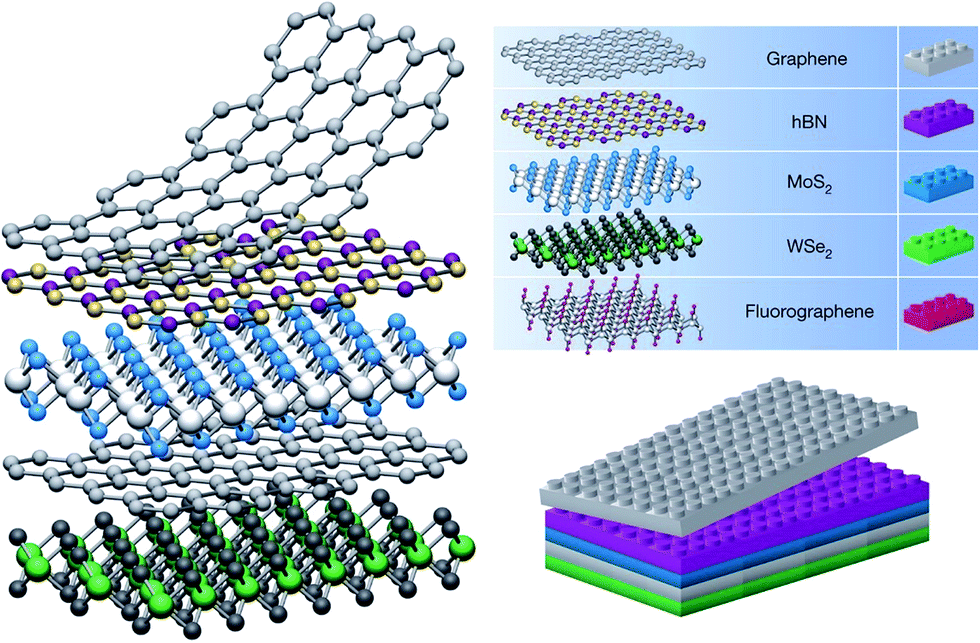
Two-dimensional (2D) materials, such as nano-films, superlattices and quantum wells, refer to the materials in which the free movement (plane motion) of electrons takes place only in the two dimensional non-nanoscale. Graphene is the most significant among all the 2D materials proposed up till now1 and has single (or several) atomic layer thickness. Beyond graphene, 2D materials also include transition metal oxides (e.g. MnO2, ZnO), transition metal carbides and/or carbonitrides (MXene), transition metal chalcogenides (e.g. MoS2), hexagonal boron nitride (h-BN), topological insulators (e.g. Bi2Se3, Sb2Te3), silicene, germanene, black phosphorus (BP) and so on (Fig. 1).2–5 2D materials as promising building blocks for novel nanoelectronics include semiconductors, insulators, transparent conductors and transducers,6–8 because amongst other considerations, these atomic sheets afford the ultimate thickness and scalability, which is desired in a variety of essential material categories. 2D semiconductors exhibit high carrier mobility, high on–off current ratio and excellent bendability that suit for future low-power consumption and flexible electronics.9–12 These materials are laterally composed of strong covalent bonds, which provide great in-plane stability. On the other hand, the weak van der Waals (vdW) interlayer forces allow us to isolate 2D monolayer and restack them into arbitrary stacking heterojunctions without the need to consider the atomic commensurability in contrast to their bulk counterparts. van der Waals (vdW)-bonded layered materials offer great variety in both structural and electronic properties, opening up new avenues for scientific research to obtain better device design and desired device functionalities by assembling heterostructures based on distinct 2D layers. Although, all-2D vdW heterostructures offer unique properties and functionalities compared with conventional devices, it still remains a challenge to produce entire families of 2D materials and their heterostructures over large areas with high electronic quality. Furthermore, control of doping type, carrier concentration and stoichiometry is quiet difficult for most 2D materials, limiting the scope and progress of all-2D vdW heterostructures.13 | ||
Fig. 1 (a) Schematic illustration of different kinds of typical ultrathin 2D nanomaterials, such as graphene, h-BN, TMDs, MOFs, COFs, MXenes, LDHs, oxides, metals, and BP. Reprinted with permission from ref. 3. Copyright 2015 ACS Publications. (b) Charge carriers in graphene are called massless Dirac fermions and are described by a 2D analog of the Dirac equation, with the Fermi velocity vF ≈ 1 × 10⁶ m s−1 playing the role of the speed of light and a 2D pseudospin ![[small sigma, Greek, vector]](https://www.rsc.org/images/entities/i_char_e1c9.gif) describing two sublattices of the honeycomb lattice. Reprinted with permission from ref. 12. Copyright 2009 AAAS. (c) TEM image, reprinted with permission from ref. 13. Copyright 2011 ACS Publications. (d) Atomic structure of graphene obtained by DFT calculation. Reprinted with permission from ref. 14. Copyright 2008 ACS Publications. (e) vdW forces in a 2D layered structure. Reprinted from http://bbc.co.uk. describing two sublattices of the honeycomb lattice. Reprinted with permission from ref. 12. Copyright 2009 AAAS. (c) TEM image, reprinted with permission from ref. 13. Copyright 2011 ACS Publications. (d) Atomic structure of graphene obtained by DFT calculation. Reprinted with permission from ref. 14. Copyright 2008 ACS Publications. (e) vdW forces in a 2D layered structure. Reprinted from http://bbc.co.uk. | ||
Graphene is the first truly 2D crystalline material, which is composed of periodic honeycomb lattice formed by sp2 hybrid orbitals of covalently bonded carbon atoms (Fig. 1b and c).12,14–17 The p orbital of coplanar carbon atoms overlap each other and form large conjugated π bonds. There is a freely moving electron at each grid point, which endow graphene to have super high electron mobility (2 × 105 cm2 V−1 s−1) at low temperature (∼5 K).1,18 Graphene is theoretically considered as zero bandgap semiconductor and the electronic conduction velocity and theoretical resistivity of graphene are 8 × 10⁵ m s−1 (ref. 19) and 10−6 Ω cm−1,20 respectively. Excellent electrical property of graphene favors the development of graphene based field effect transistors21 and the supercapacitors.22 In addition, graphene has high optical transparency23 and has broad applications in the transparent conductive thin film solar cells, photon detectors and so on,24–28 due to its unique optical properties. In addition, graphene also exhibits ultrahigh mechanical strength (1.0 TPa),29 exceptional thermal conductivity (5000 W m−1 K−1),30 half-integer quantum Hall effect at room temperature,31 Klein tunneling effect,32 and so on.
Transistors are the central device building blocks of all modern electronic systems. The first thin film transistors (TFTs) can be dated back to 1962,33 which used vacuum evaporation technique along with shadow masks to deposit gold electrodes, an n-type polycrystalline cadmium sulfide (CdS) semiconductor channel and a Si monoxide gate insulator on a glass substrate. The integration of TFTs on flexible substrates is of considerable interest for diverse applications including electronic-paper, wearable display and artificial skin, and can enable a new generation of flexible, wearable and disposable electronics.34–37 The major challenges for the realization of high performance electronics on flexible substrates are the difficulties in achieving TFTs with a high carrier mobility, high on/off ratio, low operating voltage and using a low temperature-compatible fabrication process.
The highest carrier mobility, excellent optical transparency, high mechanical strength as well as atomic thickness of graphene layers make it extremely useful for flexible FET application. Fabrication of FETs using 2D graphene crystals as an active component can significantly contribute in the evolution of next generation flexible thin film electronic devices and there have been quite a few reviews summarizing the graphene-based TFTs and their applications.38–45 Keeping in view the high demand of graphene based flexible electronics, in this review, we summarize recent development of flexible FETs based on graphene and/or graphene/semiconductor heterojunctions, consistent with the role of graphene as channel layer and/or electrodes in FETs.
2. Graphene acting as channel material in thin film transistors
For field-effect transistors (FETs), the level of its carrier mobility often determine the level of some other important performance parameters, such as current density, energy efficiency, switching delay, and so on. High mobility is beneficial to realize the maximum static control,7 optical transparency,46 sensitivity47 and flexibility,48,49 and broaden the application fields of TFTs. In this regard, graphene is one of the best choice for transparent conductive thin films in FETs, due to its excellent electronic, mechanical, optical properties and good stability as mentioned above.18,23,29Graphene transparent conductive thin films have been usually used as the conducting channel layer for graphene-based field effect transistors (GFETs). The main opportunities for graphene in both high-performance and low-power applications stem from the atomic thinness achievable in graphene-based devices, which lead to an almost perfect control of the channel potential. Very recently, Johari et al.50 have reviewed the electrical performance of GFETs using various architectures and different geometries of graphene conducting channel layer. Graphene has great advantage for its use in flexible electronics but at the same time it needs an opening of band gap for TFTs. Researchers had tried to get the good on/off ratio in graphene based FETs by fabricating the graphene as a channel layer. For example, graphene nanoribbon (a kind of graphene with width below 10 nm (ref. 51)) has been one of the most widely used conducting channel materials for GFETs. Wang et al.52 successfully synthesized graphene nanoribbons with smooth edges and size smaller than 10 nm. They demonstrated that the on/off ratio of GFETs increases with the decrease in width of graphene nanoribbon and at room temperature, the on/off ratio and carrier mobility were up to ∼1 × 10⁶ and ∼200 cm2 V−1 s−1, respectively. Processing graphene sheets into nanoribbons with widths of less than 10 nm can open up a bandgap that is large enough for room-temperature transistor operation, but nanoribbon devices often have low driving currents or transconductances. In comparison with graphene nanoribbons, the graphene nanomesh, which can be viewed as many graphene nanoribbons arrange orderly and periodically in another conducting channel material, cannot only introduce the band gap for graphene, but also dramatically increased the driving current of GFET devices.53–55 For instance, Bai et al.55 successfully obtained the graphene nanomesh with width of 5 nm, on/off ratio of the GFET based graphene nanomesh was about 100, and the current density of GFETs based graphene nanomesh was about 100 times to that of GFETs based on graphene nanoribbons. They prepared the nanomeshes with variable periodicities and neck widths as low as 5 nm using block copolymer lithography.
3. Graphene acting as electrode material in thin film transistors
The conventional electrode of field effect transistors (FETs) is mainly metal or metal oxide with limited applications as a result of their disadvantages such as insensitivity, opacity, non-flexibility as well as large contact resistance between the metal electrode and the active layer of FETs. However, graphene electrode effectively overcomes the above disadvantages of the metal electrode for FETs. Therefore, graphene transparent conductive films are widely used as an electrode material for GFETs,56–62 with a heterojunction structure between graphene electrode and the inorganic and/or organic semiconductor active layer.Heterojunctions refer to an interface between two different semiconductors (electron donor and electron acceptor), where the electronic band structure near the interface is changed according to electrostatics.63 The semiconductor heterojunctions have been applied in many solid-state devices, such as solar cells, photo detectors, semiconductor lasers, and light-emitting diodes (LEDs). In 1960, Anderson63 successfully prepared high quality heterojunctions for the first time, and provided a detailed energy band diagram and theoretical models. Due to the great influence of the semiconductor junction in our daily life, Nobel Prize in physics was awarded to Zhores I. Alferov, Herbert Kroemer and Jack S. Kilby for their contributions towards the development of semiconductor heterostructures.64–66 The weak van der Waals (vdW) interlayer forces in 2D materials allow us to isolate 2D monolayer and restack them into arbitrary stacking heterojunctions without the need to consider the atomic commensurability in contrast to their bulk counterparts. Hence, a new research field of heterojunctions formed by 2D layered materials has emerged since 2013.67 The vertically stacked 2D layers can be formed by mechanical stacking, serving as a quick and convenient way of forming heterostructures (Fig. 2). In comparison with the horizontal (lateral) heterojunction, the vertical heterojunctions usually have higher electron transition efficiency due to their larger bonding area between two different heterostructured components.
 | ||
| Fig. 2 Schematic 2D heterostructures based on van der Waals interlayer force. Reprinted with permission from ref. 67. Copyright 2013 Nature Publishing Group. | ||
3.1 Preparation of graphene/semiconductor heterojunctions
The semiconductor heterojunctions play an important role in modern electronics, being used as an essential building block of solid state devices, such as photo sensors, solar cells, light-emitting diodes and semiconductor lasers. Two-dimensional (2D) materials have the advantages of possessing unique optical bandgap structures and large surface area. Owing to the layered structures of 2D materials, the formation of heterostructures can be in vertical or lateral fashion. Depending on the architecture of the heterostructures, the fabrication methods vary. Here, we sort the fabrication processes into two categories, one is the mechanical stacking method and the other is the direct synthesis.3.2 Graphene/inorganic semiconductor heterojunction TFT
Each layer in graphene consists of a covalently bonded, dangling-bond-free lattice and is weakly bound to neighboring layers by van der Waals interactions. This makes it feasible to isolate, mix and match highly disparate atomic layers to create a wide range of van der Waals heterostructures (vdWHs) without the constraints of lattice matching and processing compatibility.69 Since the discovery of graphene, it became clear that when a graphene nanosheet is combined with some inorganic semiconductors, the zero-gap shortcomings, that limit the on/off current ratio of graphene-based transistors, could be considerably reduced or even avoided.Graphene/inorganic semiconductor heterojunctions could be classified as binary19,70–74 and ternary8,75,76 heterostructures according to the components in the heterostructures (Table 1). Graphene-based binary heterojunctions usually include graphene/h-BN,19,77 graphene/MoS2,73 graphene/WS2,70 graphene/BP,72 and so on. For example, Yu et al.73 reported the vertical integration of graphene/MoS2 heterostructures of layered materials for the fabrication of a new generation of vertical field-effect transistors (VFETs) with a room temperature on/off current ratio >103 and a high current density of up to 5000 A cm−2 (Fig. 3a and b). Subsequently, Moriya et al.71 further improved the on/off ratio and current density of the VFETs based on graphene/MoS2 heterostructures to 105 and 104 A cm−2, respectively (Fig. 3c and e).
| Year | Layer structure | Mobility/cm2 V−1 s−1 | On/off ratio | Reference |
|---|---|---|---|---|
| a Note: — indicate it is not mentioned in the references. | ||||
| 2010 | Graphene/h-BN | 6 × 10⁴ | — | 19 |
| 2012 | h-BN/graphene/h-BN/graphene/h-BN | — | 1 × 10⁴ | 78 |
| 2012 | h-BN/graphene/MoS2/graphene/h-BN | — | 50 | 78 |
| 2013 | Graphene/h-BN/MoS2 | ∼45 | 104 to 106 | 8 |
| 2013 | Graphene/WS2/graphene/h-BN | — | >1 × 10⁶ | 76 |
| 2013 | Graphene/MoS2 | — | >103 | 73 |
| 2014 | Graphene/MoS2 | — | ∼105 | 71 |
| 2014 | Graphene/h-BN/MoS2/graphene | ∼33 | >106 | 75 |
| 2015 | h-BN/graphene/h-BN | 3 × 10⁴ to 3.6 × 10⁴ | — | 74 |
| 2016 | Graphene/BP | — | ∼800 | 72 |
 | ||
| Fig. 3 Schematic illustration (a and c) and optical images (b and d) of the vertically stacked graphene/MoS2 heterostructured transistors. (e) The MoS2 layer number dependence of the Ion (current density at VB = +0.5 V and VG = +50 V) and Ioff (current density at VB = +0.5 V and VG = −50 V). Reprinted with permission from ref. 71 and 73. Copyright 2014 AIP Publishing LLC and 2013 Nature Publishing Group. | ||
Very recently, Kang et al.72 presented a vertical field-effect transistor geometry based on a graphene/black phosphorus (graphene/BP) van der Waals heterostructure (Fig. 4). The resulting device characteristics include high on-state current densities (>1600 A cm−2) and current on/off ratios exceeding 800 at low temperature. Two distinct charge transport mechanisms were identified, which are dominant for different regimes of temperature and gate voltage. In particular, the Schottky barrier between graphene and BP determines charge transport at high temperatures and positive gate voltages, whereas tunneling dominates at low temperatures and negative gate voltages.
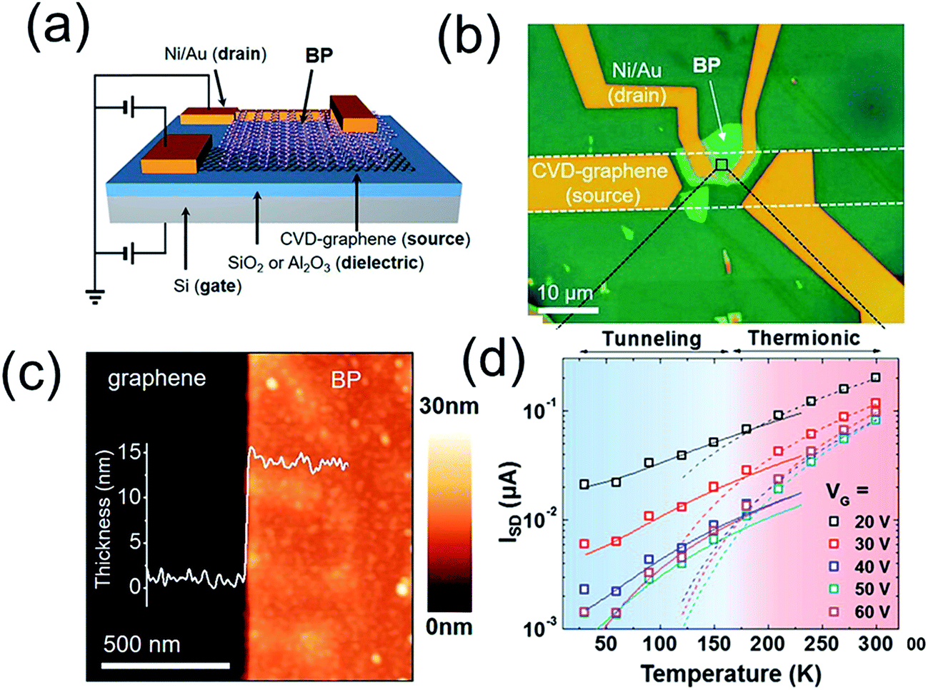 | ||
| Fig. 4 Schematic illustration (a) and optical microscopy image (b) of the BP-VFET, (c) AFM image at the edge of the BP flake. Inset: cross-sectional height profile of the BP flake on the graphene/SiO2/Si substrate, (d) temperature dependence of ISD at different gate voltages from 20 to 60 V in 10 V steps. Reprinted with permission from ref. 72. Copyright 2016 ACS. | ||
Some graphene-based ternary heterojunctions, such as graphene/h-BN/MoS2 (ref. 75) and graphene/h-BN/WS2,76 have also been reported. For example, Roy et al.75 successfully prepared a graphene/h-BN/MoS2 heterostructured TFT in which graphene was used as the electrode and contacts material and MoS2/h-BN heterojunction was used as the active layer (Fig. 5). This transistor exhibited n-type behavior with an ON/OFF current ratio of >106, and an electron mobility of ∼33 cm2 V−1 s−1. Uniquely, the mobility does not degrade at high gate voltages, presenting an important advantage over conventional Si transistors where enhanced surface roughness scattering severely reduces carrier mobilities at high gate-fields.
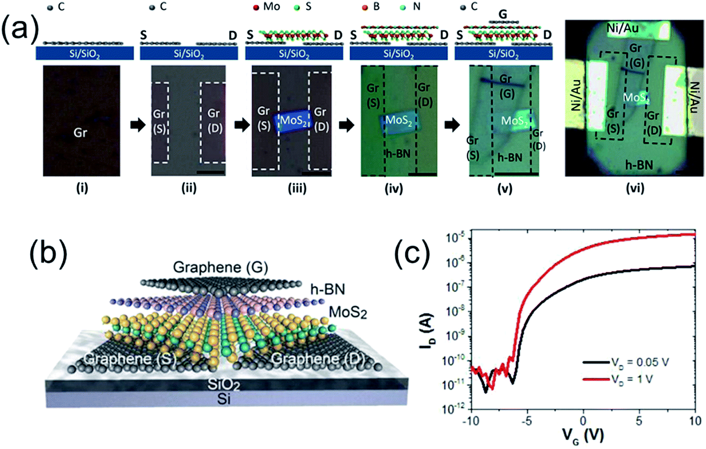 | ||
| Fig. 5 (a) Schematics (not to scale) of the fabrication process steps (top) and the corresponding optical microscope images (bottom) of a representative graphene/BN/MoS2 transistor. Scale bar is 5 μm for all images. (b and c) Schematic illustration (b) and ID–IG characteristics at different VG (c) of the graphene/BN/MoS2 transistor. Reprinted with permission from ref. 75. Copyright 2015 ACS. | ||
Lee et al.8 also reported a graphene/h-BN/MoS2 heterostructured TFT in which graphene was used as the gate electrode whereas MoS2/h-BN heterojunction was used as the active layer (Fig. 6). The high field effect mobility of 45 cm2 V−1 s−1 was achieved in trilayer MoS2 at low operating gate voltage (ΔVG < 10 V), along with no transport curve hysteresis which is due to the charge-trap-free h-BN dielectric and clean channel/dielectric interface. Moreover, due to the mechanical strength and flexibility of these materials, those FETs show unchanged performance up to 1.5% applied strain.
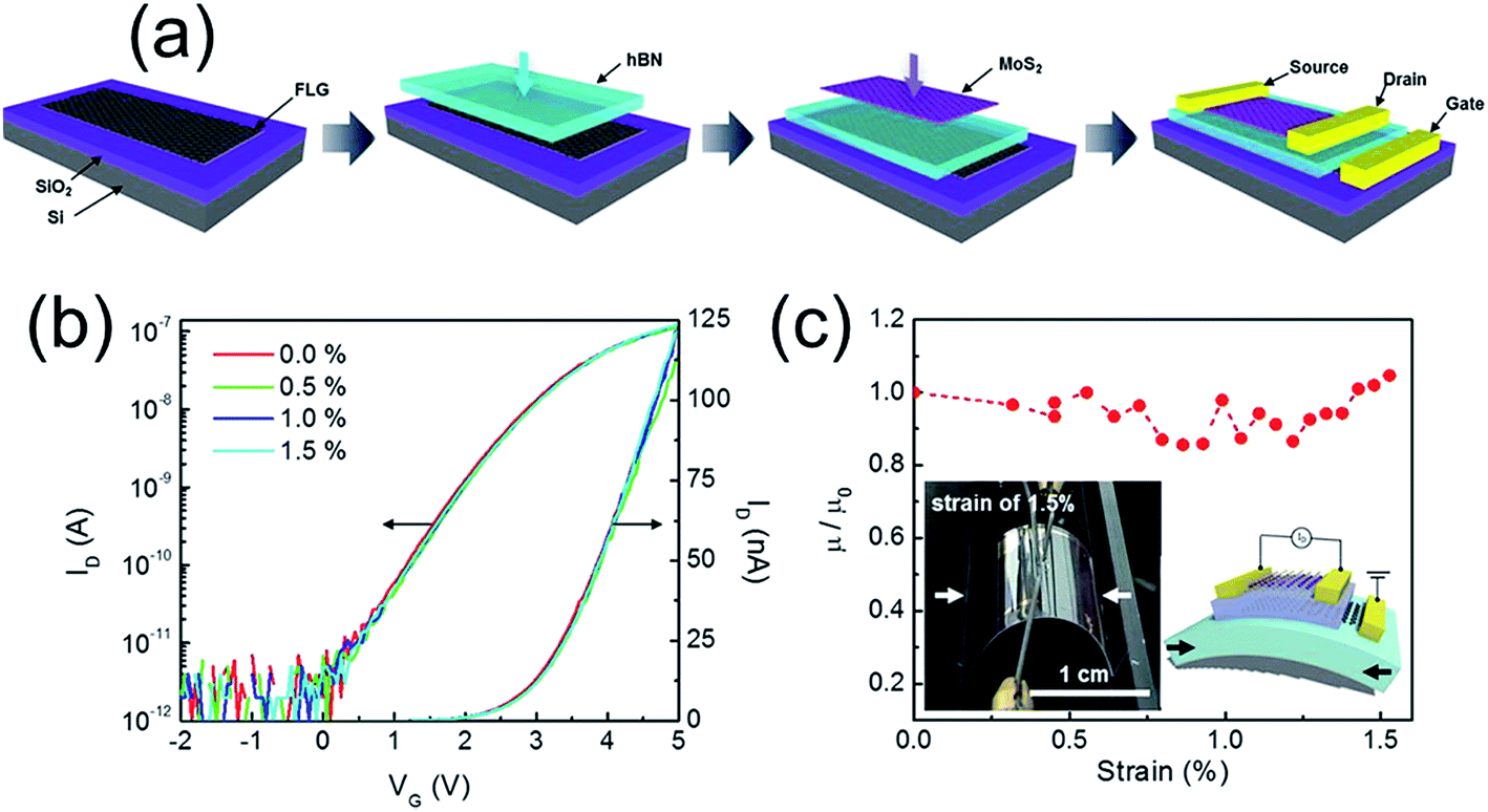 | ||
| Fig. 6 (a) Schematic of fabrication process for a graphene/BN/MoS2 transistor (b) transfer curves of the flexible graphene/BN/MoS2 transistor under different bending conditions up to 1.5% strain. (c) Relative field-effect mobility of the graphene/BN/MoS2 transistor as a function of strain. The insets show the photograph of the strained heterostructured transistor by 1.5% and schematic diagram of the strained device. The arrows in the images indicate the y-direction for strain. Reprinted with permission from ref. 8. Copyright 2013 ACS. | ||
3.3 Graphene/organic semiconductor heterojunction TFT
Electron injection barrier between the interfaces of graphene and organic materials is low,79 which makes graphene/organic hybrids to have good carrier transport behavior and high mobility. Moreover, the work function of graphene is about 4.3 eV and matches the HOMO energy level of many organic semiconductors.80,81 These are the two main reasons why vertical thin film transistors based on graphene/organic semiconductor heterojunction could obtain excellent optoelectronic properties. Graphene is usually used as electron acceptor (n-type), and the electron donor (p-type) in 2D graphene/organic semiconductor heterojunctions mainly consisting of pentacene,82–84 rubrene,82,85,86 C8-BTBT,87,88 PQT-12,89,90 P3HT91,92 and so on (Table 2).| Year | Layer structure | Mobility/cm2 V−1 s−1 | On/off ratio | Reference |
|---|---|---|---|---|
| a Note: — indicate it is not mentioned in the references. | ||||
| 2014 | Graphene/C8-BTBT | — | ∼106 | 87 |
| 2015 | Graphene/pentacene | — | >103 | 93 |
| 2015 | Graphene/pentacene | — | 8.7 × 10² | 82 |
| 2015 | Graphene/rubrene | <10 | ∼10−1 | 82 |
| 2015 | Graphene/PTCDI-C13 | — | 3.8 × 10² | 82 |
| 2015 | Graphene/C60 | — | 2.0 × 10⁴ | 82 |
| 2015 | Graphene/C60 | — | >104 | 83 |
| 2015 | Graphene/C60 | 3000 | 8 × 10⁴ | 94 |
| 2015 | Graphene/C60 | — | 3 × 10³ | 95 |
| 2015 | Graphene/P3HT | — | >103 | 91 |
Shih et al.82 synthesized a series of graphene/organic semiconductor heterostructured (e.g. graphene/pentacene, graphene/C60) vertical thin film transistors (VFETs) with good optoelectronic properties (Fig. 7 and Table 2). Interestingly, they reported the first experimental evidence that the underlying mechanism of partially screened field effect and selective carrier injection through graphene dominate the electronic transport at the organic semiconductor/graphene heterointerface. They demonstrated flexible organic/graphene VFETs with bending radius <1 mm with the output current per unit area equivalent to that of the best oxide planar FETs.
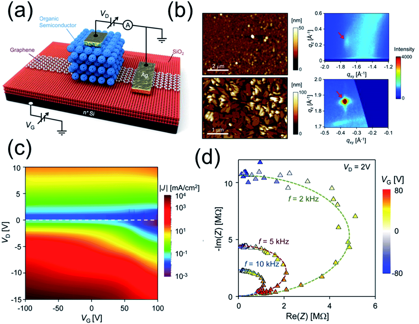 | ||
| Fig. 7 (a) Schematic of graphene/organic semiconductor heterojunction VFET device. The black connections are associated with the setup for DC measurement. (b) AFM micrographs and the (112) reflection peaks in the GIXD images for ∼100 nm PTCDI-BPE films on SiO2 (top, edge-on phase) and graphene (bottom, face-on phase). (c) Transport color maps of J as a function of VD and VG for the pentacene VFETs on as-received SiO2 substrate. (d) Trajectory of C60 impedance at fixed frequencies. By increasing VG, the C60 layer is experiencing an insulator–conductor transition, moving from a pure dielectric towards a pure conductor. Reprinted with permission from ref. 82. Copyright 2015 ACS. | ||
As shown in Fig. 8, Hlaing et al.83 reported organic thin film transistors based on vertical heterojunctions of graphene and organic semiconductors (pentacene and C60). In these thin heterostructure devices, current modulation is accomplished by tuning the injection barriers at the semiconductor/graphene interface with the application of gate voltage. N-Channel devices fabricated with a thin layer of C60 show a room temperature on/off ratio >104 and current density of up to 44 mA cm−2. Because of the intrinsic ultra-short channel in the vertical structure, the device is fully operational at a driving voltage of 200 mV.
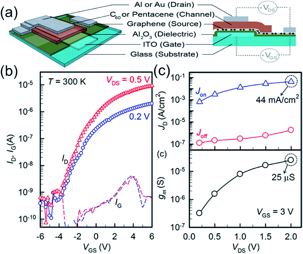 | ||
| Fig. 8 (a) Schematic illustration of the three-dimensional and cross-sectional view of the vertically stacked graphene–organic semiconductor–metal VOTFT. (b) Semi-logarithmic ID–VGS transfer characteristics of an n-type VOTFT measured at Vds values of 0.2 and 0.5 V. IG is indicated by the dashed line. (c) On- and off-current density (top) and transconductance (bottom) at various drain voltages measured at fixed gate voltage of 3 V. The active area of the transistor measured is 3 × 10⁻³ cm2. Reprinted with permission from ref. 83. Copyright 2015 ACS. | ||
Kim et al.93 demonstrated a flexible vertical Schottky Barrier (SB) transistor architecture based on a graphene–organic heterojunction and an ion gel gate dielectric. Specifically, an ion gel gate dielectric consisting of an ionic liquid within a network polymer was used to modulate the SB formed at the graphene–organic (p-type pentacene or n-type N,N′-dioctyl-3,4,9,10-perylenedicarboximide) heterojunction upon application of a bias at the gate located parallel to the source electrode. The resulting p- and n-type devices could be successfully operated at voltages below 1 V while yielding a high current density in excess of 100 mA cm−2 and a high on/off current ratio greater than 103.
Liu et al.91 fabricated high-performance organic vertical thin film transistors (OVTFTs) based on graphene/organic semiconducting (P3HT, PBT7 and PCBM) thin film heterostructures through a general strategy of OVTFT fabrication with ultra-short channel length without using conventional high-resolution lithography processes (Fig. 9). Electrical studies show that those vertical transistors exhibit excellent switching behavior with an ON/OFF ratio greater than 103 and a high current density greater than 3.4 A cm−2, and thus enable high cutoff frequency devices comparable to planar ultra-short channel organic transistors.
 | ||
| Fig. 9 (a) Schematic illustration of the cross-sectional view of the OVTFT device (b) cross-sectional SEM image of an OVTFT, clearly illustrating layers of the vertical stack. The scale bar is 100 nm. (c) Ids–Vds output characteristics of a graphene–P3HT–Au p-type OVTFTs at various gate voltages from −30 to +30 V (15 V steps). The transfer curve is semilog-plotted in the insets with various bias voltages where Vds = −1 V (blue), −2 V (red), and −4 V (black). (d) Transfer characteristics of an OVTFT on glass at different bias voltages from −1 to −9 V (1 V steps). (e) Transconductance as a function of the gate voltage at different bias voltages. (f) Gate and drain AC current as a function of input frequency signal. The red dot is the measured drain current, and the black square is the measured gate current. The blue triangle is the calibrated gate current by considering the effective gate area and gate capacitance. Reprinted with permission from ref. 91. Copyright 2015 ACS. | ||
4. Conclusions and outlook
In this review, we have attempted to summarize recent development of flexible thin film transistors (TFT) based on graphene and graphene/semiconductor heterostructures according to the role of graphene which act as electrodes material as well as a channel layer in FET. Especially, we reviewed the progress of TFTs based on graphene/semiconductor (including inorganic and organic semiconductors) heterojunctions in which graphene act as electrodes materials in detail. It must be recognized that there are many caveats and challenges. For example, although the channel material itself may be atomically thin, electric field lines can extend from the drain to the source through the underlying buried oxide, leading to drain-induced barrier lowering, or through the high-k gate dielectric, leading to so-called fringing-field-induced barrier lowering. On the other hand, there are still many challenges ahead in creating large-area and very flat (<0.2 nm surface roughness) 2D films, although graphene single crystals up to 5 cm in diameter have been grown on hydrogen-terminated germanium.96 Certainly, graphene needs various technological issues to overcome, nevertheless it looks promising for flexible electronic applications, which are difficult to realize with conventional materials. In future, large-area integration of 2D materials, specifically graphene, with materials of other dimensionality is likely to have a sizable impact on semiconductor technologies. Furthermore, single-crystalline film quality and thickness uniformity with minimal cracks, voids, wrinkles, ripples and other contaminants are critical. Therefore, direct synthesis of high-quality 2D materials on insulating substrates should be a high priority. Overall, the vast integration possibilities presented by mixed-dimensional vdW heterostructures suggest considerable future growth potential for this field in both fundamental studies and applied technologies. It is anticipated that further progress in 2D material growth, heterostructure formation and device fabrication shall lead to practical applications in future.Acknowledgements
This work was supported by Natural National Science Foundation of China and Pakistan Science Foundation Collaborative research project (5161101159), Guangdong Talents Project, NSFC (51373075, 61136003) National Basic Research Program of China (973 Program, No. 2015CB856505; 2015CB93220), Natural Science Foundation of Jiangsu Province (BM2012010), the Shenzhen Peacock Program (KQTD2014062714543296) and Shenzhen Key Laboratory of Shenzhen Science and Technology Plan (ZDSYS20140509094114164).References
- K. S. Novoselov, A. K. Geim, S. V. Morozov, D. Jiang, Y. Zhang, S. V. Dubonos, I. V. Grigorieva and A. A. Firsov, Science, 2004, 306(5696), 666–669 CrossRef CAS PubMed.
- G. R. Bhimanapati, Z. Lin, V. Meunier, Y. Jung, J. Cha, S. Das, D. Xiao, Y. Son, M. S. Strano, V. R. Cooper, L. Liang, S. G. Louie, E. Ringe, W. Zhou, S. S. Kim, R. R. Naik, B. G. Sumpter, H. Terrones, F. Xia, Y. Wang, J. Zhu, D. Akinwande, N. Alem, J. A. Schuller, R. E. Schaak, M. Terrones and J. A. Robinson, ACS Nano, 2015, 9(12), 11509–11539 CrossRef CAS PubMed.
- H. Zhang, ACS Nano, 2015, 9(10), 9451–9469 CrossRef CAS PubMed.
- C. N. R. Rao, H. S. S. R. Matte and U. Maitra, Angew. Chem., Int. Ed., 2013, 52(50), 13162–13185 CrossRef CAS PubMed.
- A. Gupta, T. Sakthivel and S. Seal, Prog. Mater. Sci., 2015, 73, 44–126 CrossRef CAS.
- I. Meric, C. R. Dean, N. Petrone, L. Wang, J. Hone, P. Kim and K. L. Shepard, Proc. IEEE, 2013, 101(7), 1609–1619 CrossRef CAS.
- H. Fang, S. Chuang, T. C. Chang, K. Takei, T. Takahashi and A. Javey, Nano Lett., 2012, 12(7), 3788–3792 CrossRef CAS PubMed.
- G.-H. Lee, Y.-J. Yu, X. Cui, N. Petrone, C.-H. Lee, M. S. Choi, D.-Y. Lee, C. Lee, W. J. Yoo, K. Watanabe, T. Taniguchi, C. Nuckolls, P. Kim and J. Hone, ACS Nano, 2013, 7(9), 7931–7936 CrossRef CAS PubMed.
- B. Radisavljevic, A. Radenovic, J. Brivio, V. Giacometti and A. Kis, Nat. Nanotechnol., 2011, 6(3), 147–150 CrossRef CAS PubMed.
- Q. Y. He, Z. Y. Zeng, Z. Y. Yin, H. Li, S. X. Wu, X. Huang and H. Zhang, Small, 2012, 8(19), 2994–2999 CrossRef CAS PubMed.
- J. Pu, Y. Yomogida, K.-K. Liu, L.-J. Li, Y. Iwasa and T. Takenobu, Nano Lett., 2012, 12(8), 4013–4017 CrossRef CAS PubMed.
- A. K. Geim, Science, 2009, 324(5934), 1530–1534 CrossRef CAS PubMed.
- D. Jariwala, T. J. Marks and M. C. Hersam, Nat. Mater., 2017, 16(2), 170–181 CrossRef CAS PubMed.
- J. C. Meyer, C. Kisielowski, R. Erni, M. D. Rossell, M. F. Crommie and A. Zettl, Nano Lett., 2008, 8(11), 3582–3586 CrossRef CAS PubMed.
- A. K. Geim and K. S. Novoselov, Nat. Mater., 2007, 6(3), 183–191 CrossRef CAS PubMed.
- K. S. Novoselov, V. I. Fal'ko, L. Colombo, P. R. Gellert, M. G. Schwab and K. Kim, Nature, 2012, 490(7419), 192–200 CrossRef CAS PubMed.
- K. S. Novoselov, A. K. Geim, S. V. Morozov, D. Jiang, M. I. Katsnelson, I. V. Grigorieva, S. V. Dubonos and A. A. Firsov, Nature, 2005, 438(7065), 197–200 CrossRef CAS PubMed.
- K. I. Bolotin, K. J. Sikes, Z. Jiang, M. Klima, G. Fudenberg, J. Hone, P. Kim and H. L. Stormer, Solid State Commun., 2008, 146(9–10), 351–355 CrossRef CAS.
- C. R. Dean, A. F. Young, I. Meric, C. Lee, L. Wang, S. Sorgenfrei, K. Watanabe, T. Taniguchi, P. Kim, K. L. Shepard and J. Hone, Nat. Nanotechnol., 2010, 5(10), 722–726 CrossRef CAS PubMed.
- J.-H. Chen, C. Jang, S. Xiao, M. Ishigami and M. S. Fuhrer, Nat. Nanotechnol., 2008, 3(4), 206–209 CrossRef CAS PubMed.
- S. Hertel, D. Waldmann, J. Jobst, A. Albert, M. Albrecht, S. Reshanov, A. Schoner, M. Krieger and H. B. Weber, Nat. Commun., 2012, 3, 957 CrossRef CAS PubMed.
- M. F. El-Kady, V. Strong, S. Dubin and R. B. Kaner, Science, 2012, 335(6074), 1326–1330 CrossRef CAS PubMed.
- R. R. Nair, P. Blake, A. N. Grigorenko, K. S. Novoselov, T. J. Booth, T. Stauber, N. M. R. Peres and A. K. Geim, Science, 2008, 320(5881), 1308 CrossRef CAS PubMed.
- J. Lu, J.-x. Yang, J. Wang, A. Lim, S. Wang and K. P. Loh, ACS Nano, 2009, 3(8), 2367–2375 CrossRef CAS PubMed.
- G. Eda and M. Chhowalla, Adv. Mater., 2010, 22(22), 2392–2415 CrossRef CAS PubMed.
- H. Liu, T. Ye and C. Mao, Angew. Chem., Int. Ed., 2007, 46(34), 6473–6475 CrossRef CAS PubMed.
- C.-H. Lu, H.-H. Yang, C.-L. Zhu, X. Chen and G.-N. Chen, Angew. Chem., Int. Ed., 2009, 48(26), 4785–4787 CrossRef CAS PubMed.
- Y.-R. Chang, H.-Y. Lee, K. Chen, C.-C. Chang, D.-S. Tsai, C.-C. Fu, T.-S. Lim, Y.-K. Tzeng, C.-Y. Fang, C.-C. Han, H.-C. Chang and W. Fann, Nat. Nanotechnol., 2008, 3(5), 284–288 CrossRef CAS PubMed.
- C. Lee, X. Wei, J. W. Kysar and J. Hone, Science, 2008, 321(5887), 385–388 CrossRef CAS PubMed.
- A. A. Balandin, S. Ghosh, W. Bao, I. Calizo, D. Teweldebrhan, F. Miao and C. N. Lau, Nano Lett., 2008, 8(3), 902–907 CrossRef CAS PubMed.
- K. S. Novoselov, Z. Jiang, Y. Zhang, S. V. Morozov, H. L. Stormer, U. Zeitler, J. C. Maan, G. S. Boebinger, P. Kim and A. K. Geim, Science, 2007, 315(5817), 1379 CrossRef CAS PubMed.
- M. I. Katsnelson, K. S. Novoselov and A. K. Geim, Nat. Phys., 2006, 2(9), 620–625 CrossRef CAS.
- P. K. Weimer, Proc. IRE, 1962, 50(6), 1462–1469 CrossRef.
- A. Dodabalapur, Mater. Today, 2006, 9(4), 24–30 CrossRef CAS.
- T. Someya, Y. Kato, T. Sekitani, S. Iba, Y. Noguchi, Y. Murase, H. Kawaguchi and T. Sakurai, Proc. Natl. Acad. Sci. U. S. A., 2005, 102(35), 12321–12325 CrossRef CAS PubMed.
- J. A. Rogers, Z. Bao, K. Baldwin, A. Dodabalapur, B. Crone, V. R. Raju, V. Kuck, H. Katz, K. Amundson, J. Ewing and P. Drzaic, Proc. Natl. Acad. Sci. U. S. A., 2001, 98(9), 4835–4840 CrossRef CAS PubMed.
- A. Schlierf, P. Samori and V. Palermo, J. Mater. Chem. C, 2014, 2(17), 3129–3143 RSC.
- B. K. Sharma and J. H. Ahn, Solid-State Electron., 2013, 89, 177–188 CrossRef CAS.
- D. Akinwande, N. Petrone and J. Hone, Nat. Commun., 2014, 5, 5678 CrossRef CAS PubMed.
- G. Fiori, F. Bonaccorso, G. Iannaccone, T. Palacios, D. Neumaier, A. Seabaugh, S. K. Banerjee and L. Colombo, Nat. Nanotechnol., 2014, 9(10), 768–779 CrossRef CAS PubMed.
- S. J. Park, O. S. Kwon, S. H. Lee, H. S. Song, T. H. Park and J. Jang, Nano Lett., 2012, 12(10), 5082–5090 CrossRef CAS PubMed.
- C. Sire, F. Ardiaca, S. Lepilliet, J. W. T. Seo, M. C. Hersam, G. Darnbrine, H. Happy and V. Derycke, Nano Lett., 2012, 12(3), 1184–1188 CrossRef CAS PubMed.
- C. Biswas and Y. H. Lee, Adv. Funct. Mater., 2011, 21(20), 3806–3826 CrossRef CAS.
- Q. Y. He, S. X. Wu, Z. Y. Yin and H. Zhang, Chem. Sci., 2012, 3(6), 1764–1772 RSC.
- B. B. Zhan, C. Li, J. Yang, G. Jenkins, W. Huang and X. C. Dong, Small, 2014, 10(20), 4042–4065 CAS.
- S. Lee, K. Lee, C.-H. Liu, G. S. Kulkarni and Z. Zhong, Nat. Commun., 2012, 3, 1018 CrossRef PubMed.
- Q. H. Wang, K. Kalantar-Zadeh, A. Kis, J. N. Coleman and M. S. Strano, Nat. Nanotechnol., 2012, 7(11), 699–712 CrossRef CAS PubMed.
- J. Lee, T.-J. Ha, H. Li, K. N. Parrish, M. Holt, A. Dodabalapur, R. S. Ruoff and D. Akinwande, ACS Nano, 2013, 7(9), 7744–7750 CrossRef CAS PubMed.
- R. C. Cooper, C. Lee, C. A. Marianetti, X. Wei, J. Hone and J. W. Kysar, Phys. Rev. B: Condens. Matter Mater. Phys., 2013, 87(3), 035423 CrossRef.
- Z. Johari and R. Ismail, Sci. Adv. Mater., 2015, 7(10), 2011–2020 CrossRef CAS.
- X. Li, X. Wang, L. Zhang, S. Lee and H. Dai, Science, 2008, 319(5867), 1229–1232 CrossRef CAS PubMed.
- X. Wang, Y. Ouyang, X. Li, H. Wang, J. Guo and H. Dai, Phys. Rev. Lett., 2008, 100(20), 1586–1594 CrossRef PubMed.
- S. Berrada, N. Viet Hung, D. Querlioz, J. St-Martin, A. Alarcon, C. Chassat, A. Bournel and P. Dollfus, Appl. Phys. Lett., 2013, 103(18), 183509 CrossRef.
- I. Jung, H. Y. Jang, J. Moon and S. Park, Nanoscale, 2014, 6(12), 6482–6486 RSC.
- J. Bai, X. Zhong, S. Jiang, Y. Huang and X. Duan, Nat. Nanotechnol., 2010, 5(3), 190–194 CrossRef CAS PubMed.
- Y. Song, W. Fang, R. Brenes and J. Kong, Nano Today, 2015, 10(6), 681–700 CrossRef CAS.
- C.-a. Di, D. Wei, G. Yu, Y. Liu, Y. Guo and D. Zhu, Adv. Mater., 2008, 20(17), 3289–3293 CrossRef CAS.
- G. Wang, Y. Kim, M. Choe, T.-W. Kim and T. Lee, Adv. Mater., 2011, 23(6), 755–760 CrossRef CAS PubMed.
- H. Chang, G. Wang, A. Yang, X. Tao, X. Liu, Y. Shen and Z. Zheng, Adv. Funct. Mater., 2010, 20(17), 2893–2902 CrossRef CAS.
- W. Liu, B. L. Jackson, J. Zhu, C.-Q. Miao, C.-H. Chung, Y.-J. Park, K. Sun, J. Woo and Y.-H. Xie, ACS Nano, 2011, 5(3), 2412 CrossRef CAS.
- J. Y. Choi, W. Kang, B. Kang, W. Cha, S. K. Son, Y. Yoon, H. Kim, Y. Kang, M. J. Ko, H. J. Son, K. Cho, J. H. Cho and B. Kim, ACS Appl. Mater. Interfaces, 2015, 7(10), 6002–6012 CAS.
- W. H. Lee, J. Park, S. H. Sim, S. B. Jo, K. S. Kim, B. H. Hong and K. Cho, Adv. Mater., 2011, 23(15), 1752–1756 CrossRef CAS PubMed.
- R. L. Anderson, Solid-State Electron., 1962, 5(SEP-O), 341–344 CrossRef CAS.
- Z. I. Alferov, V. M. Andreev, D. Z. Garbuzov, Y. V. Zhilyaev, E. P. Morozov, E. L. Portnoi and V. G. Trofim, Fiz. Tekh. Poluprovodn., 1970, 4(9), 1826–1829 CAS.
- I. Hayashi, M. B. Panish and P. W. Foy, IEEE J. Quantum Electron., 1969, 5(4), 211–212 CrossRef.
- H. Kressel and H. Nelson, RCA Rev., 1969, 30(1), 106–113 CAS.
- A. K. Geim and I. V. Grigorieva, Nature, 2013, 499(7459), 419–425 CrossRef CAS PubMed.
- Y. Shi, W. Zhou, A.-Y. Lu, W. Fang, Y.-H. Lee, A. L. Hsu, S. M. Kim, K. K. Kim, H. Y. Yang, L.-J. Li, J.-C. Idrobo and J. Kong, Nano Lett., 2012, 12(6), 2784–2791 CrossRef CAS PubMed.
- Y. Liu, N. O. Weiss, X. Duan, H.-C. Cheng, Y. Huang and X. Duan, Nat. Rev. Mater., 2016, 16042 CrossRef CAS.
- H. Tan, Y. Fan, Y. Rong, B. Porter, C. S. Lau, Y. Zhou, Z. He, S. Wang, H. Bhaskaran and J. H. Warner, ACS Appl. Mater. Interfaces, 2016, 8(3), 1644–1652 CAS.
- R. Moriya, T. Yamaguchi, Y. Inoue, S. Morikawa, Y. Sata, S. Masubuchi and T. Machida, Appl. Phys. Lett., 2014, 105(8), 083119 CrossRef.
- J. Kang, D. Jariwala, C. R. Ryder, S. A. Wells, Y. Choi, E. Hwang, J. H. Cho, T. J. Marks and M. C. Hersam, Nano Lett., 2016, 16(4), 2580–2585 CrossRef CAS PubMed.
- W. J. Yu, Z. Li, H. Zhou, Y. Chen, Y. Wang, Y. Huang and X. Duan, Nat. Mater., 2013, 12(3), 246–252 CrossRef CAS PubMed.
- M. A. Stolyarov, G. Liu, S. L. Rumyantsev, M. Shur and A. A. Balandin, Appl. Phys. Lett., 2015, 107(2), 023106 CrossRef.
- T. Roy, M. Tosun, J. S. Kang, A. B. Sachid, S. B. Desai, M. Hettick, C. C. Hu and A. Javey, ACS Nano, 2014, 8(6), 6259–6264 CrossRef CAS PubMed.
- T. Georgiou, R. Jalil, B. D. Belle, L. Britnell, R. V. Gorbachev, S. V. Morozov, Y.-J. Kim, A. Gholinia, S. J. Haigh, O. Makarovsky, L. Eaves, L. A. Ponomarenko, A. K. Geim, K. S. Novoselov and A. Mishchenko, Nat. Nanotechnol., 2013, 8(2), 100–103 CrossRef CAS PubMed.
- S. J. Kang, G.-H. Lee, Y.-J. Yu, Y. Zhao, B. Kim, K. Watanabe, T. Taniguchi, J. Hone, P. Kim and C. Nuckolls, Adv. Funct. Mater., 2014, 24(32), 5157–5163 CrossRef CAS.
- L. Britnell, R. V. Gorbachev, R. Jalil, B. D. Belle, F. Schedin, A. Mishchenko, T. Georgiou, M. I. Katsnelson, L. Eaves, S. V. Morozov, N. M. R. Peres, J. Leist, A. K. Geim, K. S. Novoselov and L. A. Ponomarenko, Science, 2012, 335(6071), 947–950 CrossRef CAS PubMed.
- S. Lee, G. Jo, S.-J. Kang, G. Wang, M. Choe, W. Park, D.-Y. Kim, Y. H. Kahng and T. Lee, Adv. Mater., 2011, 23(1), 100–105 CrossRef CAS PubMed.
- Y. Shi, K. K. Kim, A. Reina, M. Hofmann, L.-J. Li and J. Kong, ACS Nano, 2010, 4(5), 2689–2694 CrossRef CAS PubMed.
- Y.-J. Yu, Y. Zhao, S. Ryu, L. E. Brus, K. S. Kim and P. Kim, Nano Lett., 2009, 9(10), 3430–3434 CrossRef CAS PubMed.
- C.-J. Shih, R. Pfattner, Y.-C. Chiu, N. Liu, T. Lei, D. Kong, Y. Kim, H.-H. Chou, W.-G. Bae and Z. Bao, Nano Lett., 2015, 15(11), 7587–7595 CrossRef CAS PubMed.
- H. Hlaing, C.-H. Kim, F. Carta, C.-Y. Nam, R. A. Barton, N. Petrone, J. Hone and I. Kymissis, Nano Lett., 2015, 15(1), 69–74 CrossRef CAS PubMed.
- D. Jariwala, S. L. Howell, K.-S. Chen, J. Kang, V. K. Sangwan, S. A. Filippone, R. Turrisi, T. J. Marks, L. J. Lauhon and M. C. Hersam, Nano Lett., 2016, 16(1), 497–503 CrossRef CAS PubMed.
- C.-H. Lee, T. Schiros, E. J. G. Santos, B. Kim, K. G. Yager, S. J. Kang, S. Lee, J. Yu, K. Watanabe, T. Taniguchi, J. Hone, E. Kaxiras, C. Nuckolls and P. Kim, Adv. Mater., 2014, 26(18), 2812–2817 CrossRef CAS PubMed.
- F. Liu, W. L. Chow, X. He, P. Hu, S. Zheng, X. Wang, J. Zhou, Q. Fu, W. Fu, P. Yu, Q. Zeng, H. J. Fan, B. K. Tay, C. Kloc and Z. Liu, Adv. Funct. Mater., 2015, 25(36), 5865–5871 CrossRef CAS.
- D. He, Y. Zhang, Q. Wu, R. Xu, H. Nan, J. Liu, J. Yao, Z. Wang, S. Yuan, Y. Li, Y. Shi, J. Wang, Z. Ni, L. He, F. Miao, F. Song, H. Xu, K. Watanabe, T. Taniguchi, J.-B. Xu and X. Wang, Nat. Commun., 2014, 5, 5162 CrossRef CAS PubMed.
- D. He, Y. Pan, H. Nan, S. Gu, Z. Yang, B. Wu, X. Luo, B. Xu, Y. Zhang, Y. Li, Z. Ni, B. Wang, J. Zhu, Y. Chai, Y. Shi and X. Wang, Appl. Phys. Lett., 2015, 107(18), 183103 CrossRef.
- J. Huang, D. R. Hines, B. J. Jung, M. S. Bronsgeest, A. Tunnell, V. Ballarotto, H. E. Katz, M. S. Fuhrer, E. D. Williams and J. Cumings, Org. Electron., 2011, 12(9), 1471–1476 CrossRef CAS.
- C. Derry, Y. Wu, S. Gardner and S. Zhu, ACS Appl. Mater. Interfaces, 2014, 6(22), 20269–20275 CAS.
- Y. Liu, H. Zhou, N. O. Weiss, Y. Huang and X. Duan, ACS Nano, 2015, 9(11), 11102–11108 CrossRef CAS PubMed.
- P.-H. Ho, S.-S. Li, Y.-T. Liou, C.-Y. Wen, Y.-H. Chung and C.-W. Chen, Adv. Mater., 2015, 27(2), 282–287 CrossRef CAS PubMed.
- B. J. Kim, E. Hwang, M. S. Kang and J. H. Cho, Adv. Mater., 2015, 27(39), 5875–5881 CrossRef CAS PubMed.
- S. Parui, L. Pietrobon, D. Ciudad, S. Velez, X. Sun, F. Casanova, P. Stoliar and L. E. Hueso, Adv. Funct. Mater., 2015, 25(20), 2972–2979 CrossRef CAS.
- K. Kim, T. H. Lee, E. J. G. Santos, P. S. Jo, A. Salleo, Y. Nishi and Z. Bao, ACS Nano, 2015, 9(6), 5922–5928 CrossRef CAS PubMed.
- B. Wu, Y. Zhao, H. Nan, Z. Yang, Y. Zhang, H. Zhao, D. He, Z. Jiang, X. Liu, Y. Li, Y. Shi, Z. Ni, J. Wang, J.-B. Xu and X. Wang, Nano Lett., 2016, 16(6), 3754–3759 CrossRef CAS PubMed.
Footnote |
| † First co-authors with equal contribution. |
| This journal is © The Royal Society of Chemistry 2017 |