
 Open Access Article
 This Open Access Article is licensed under a Creative Commons Attribution-Non Commercial 3.0 Unported Licence
Vertically aligned ZnO/ZnTe core/shell heterostructures on an AZO substrate for improved photovoltaic performance†
Songping Luoa,
Xiaoli Hea,
Heping Shena,
Jianbao Liab,
Xuewen Yina,
Dan Oron*c and
Hong Lin *a
*a
aState Key Laboratory of New Ceramics & Fine Processing, School of Materials Science and Engineering, Tsinghua University, Beijing 100084, China. E-mail: hong-lin@tsinghua.edu.cn
bKey Laboratory of Ministry of Education for Application Technology of Chemical Materials in Hainan Superior Resources, College of Materials Science and Chemical Engineering, Hainan University, Hainan 570228, China
cDepartment of Physics of Complex Systems, Weizmann Institute of Science, Rehovot 76100, Israel. E-mail: dan.oron@weizmann.ac.il
First published on 7th March 2017
Abstract
Vertically aligned ZnO/ZnTe core/shell heterostructures on an Al-doped ZnO substrate are developed for non-toxic semiconductor sensitized solar cells. Structural and morphological analysis serves as evidence of the successful synthesis of ZnO nanorods, ZnTe nanocrystals and ZnO/ZnTe heterostructures. The clearly observed quenching of photoluminescence (PL) from the heterostructure indicates efficient charge transfer occurring at the interface of ZnO and ZnTe, due to the type-II energy level alignment constructed by the two. The formation mechanism of the ZnO/ZnTe heterostructure is studied in depth via time-dependent reactions. It was found that the strain between ZnO and ZnTe modifies the band alignment at the interface of the heterostructure in a manner which depends on the growth time. Finally, sensitized solar cells based on the ZnO/ZnTe heterostructures with different ZnTe growth times were fabricated to evaluate the photovoltaic performance. By the careful control of the ZnTe growth time and as a result of the band alignment between ZnO and ZnTe, the power conversion efficiency (PCE) of the vertically aligned ZnO/ZnTe based solar cells could be improved to about 2%, along with a short-circuit photocurrent density of around 7.5 mA cm−2, a record efficiency for ZnO/ZnTe based sensitized solar cells. Notably, for the optimized system the internal quantum efficiency of the ZnO/ZnTe based solar cell approaches 100% in certain wavelengths, implying effective separation of photoexcited free carriers towards either the electrolyte or anode.
1. Introduction
Semiconductor sensitized solar cells (SSSCs) are one of the most studied types of next generation of solar cells, along with dye-sensitized solar cells,1 polymer solar cells2 and the emerging organo-lead-halide perovskite cells.3,4 The efficiency of SSSCs' has improved dramatically over the last few years, recently exceeding 10%.5 Yet, high efficiency SSSCs utilize PbS,5 CdS,6 CdSe,7 CdSeTe8 as sensitizers, all of which contain toxic heavy metals – mostly lead and cadmium. This clearly raises significant issues regarding their potential practical application, and highlights the need to develop more environmentally friendly SSSC materials and designs.ZnTe, having a bulk band gap of about 2.25 eV, is one potential contender for non-toxic SSSCs. It has been shown both theoretically and experimentally that ZnO/ZnTe heterostructures could serve as photoanodes in photovoltaic devices. Moreover, the band alignment between the two materials can be modified by strain, which may depend on the growth method.9,10 ZnO/ZnTe heterostructures based on vertically grown nanowires have previously been fabricated by CVD.11 We have recently reported a simpler, low-cost approach to synthesize ZnO/ZnTe heterostructures by using dendrite-like ZnO nanorods as sacrificial templates via an in situ method.10 These devices exhibited good absorption properties due to the effect of light scattering, reaching an overall efficiency of up to 1.7%. Yet, the geometry of the dendrite-like ZnO is probably inferior to vertically grown wires in terms of charge transport due to the loose contact between ZnO nanorods and the transparent conductive glass (fluorine-doped SnO2, FTO). Indeed, sensitized solar cells made from oriented, one-dimensional semiconductor nanostructures have been shown to improve the cell photovoltaic performance, attributed to the direct connection of the point of photogeneration with the collection electrode.12,13 This was shown for chemical bath deposited ZnO nanorods based semiconductor sensitized cells14,15 as well as for vertically oriented single crystal rutile TiO2 nanowire based dye sensitized cells.13 It can thus be anticipated that ZnTe-based SSSC's could exhibit improved performance when based on vertically grown wires. Since, as discussed above, the band alignment between ZnO and ZnTe can be modified by strain, it is necessary to carry out a systematic study of the band alignment when considering a new geometry for the photoanode.
Here, we perform such a systematic study of ZnO/ZnTe heterostructures based on vertically grown nanorods. The vertically aligned ZnO nanorods were grown by a chemical bath deposition (CBD) method, taking Al-doped ZnO (AZO) glass as both a layer of ZnO seeds and substrate. ZnTe was grown in situ using wet chemical methods on the sacrificial ZnO template. Several samples with different growth times were prepared and studied as a function of the growth time. The formation mechanism of ZnO/ZnTe heterostructure was studied via time-dependent reactions and relevant transmission electron microscopy (TEM) measurements. Structural, morphological analyses and photoluminescence (PL) measurements were then performed in detail to investigate the properties of the as prepared samples. In particular, the band structures of the fabricated ZnO/ZnTe heterostructures with different ZnTe growth times were studied by absorption measurements and X-ray photoelectron spectroscopy (XPS) spectra. Finally, SSSCs based on the ZnO/ZnTe heterostructure with different ZnTe growth time were fabricated, for which the charge transport and recombination processes have also been investigated in detail by electrochemical impedance spectroscopy (EIS). The best performing device indeed showed an improvement in efficiency as compared with cells utilizing dendrite-like ZnO structures.
2. Experimental
2.1 Synthesis of ZnO nanorods, ZnO/ZnTe core/shell heterostructures and ZnTe nanocrystals
ZnO nanorods were grown by immersing the thoroughly cleaned AZO glass in an aqueous solution containing zinc nitrate hydrate (0.1 M), hexamethylenetetramine (0.1 M), and polyethylenimine (5.0 mM) at 90 °C for 4 h. The ZnO nanorod samples were then thoroughly rinsed with deionized water, ethanol to remove the surfactant and the residual salt and annealed at 350 °C for 20 min in air to increase the conductivity.The ZnO/ZnTe core/shell heterostructure was prepared according to the method in our previous publication.10 Briefly, the ZnO nanorods were kept in a 16 mM Te2− source solution for a period of time at 50 °C for 6 h in a sealed box. Te2− source solution was prepared by dissolving Te powder and NaBH4 in water. In order to study the properties of ZnTe alone, ZnTe nanocrystals were prepared by keeping the prepared ZnO nanorods in Te2− source solution at 50 °C for over 18 h to completely remove the inner ZnO cores.
2.2 Device fabrication
The counter electrode was prepared by sputtering platinum onto the FTO glass. The cells were fabricated by assembling counter electrodes and respective ZnO/ZnTe based photoanodes (active cell area of 0.4 × 0.4 cm2) with a 60 μm thick Surlyn hotmelt ring (DuPont, USA). The electrolyte consisted of 0.025 M I2, 0.6 M 1-propyl-3-methylimidazolium iodide (PMII), 0.1 M guanidine thiocyanate (GNCS), and 0.5 M 4-tert-butylpyridine (TBP) in acetonitrile (AN). When measuring the cell performance, the electrolyte was injected.2.3 Characterization
The morphology of the samples was characterized by field emission scanning electron microscope (SEM: LEO 1530, Gemini, Zeiss, Germany). High resolution transmission electron microscopy (HRTEM) measurements were performed by a JEM-2100 electron microscope (JEOL, Japan). X-ray diffractometer (XRD, D8 advance, Bruker, Germany) was used to determine the structural properties of the as prepared samples. The vibrational properties of the samples were investigated by the Raman spectroscopy (HORIBA JOBIN YVON HR800, France) excited by a 488 nm laser at room temperature. X-ray photoelectron spectroscopy (XPS) spectra were performed on X-ray photoelectron spectrometer (ESCALAB 250Xi, Thermo Fisher SCIENTIFIC INC., USA). The absorption properties were obtained by measuring with a UV/VIS/NIR Spectrophotometer (Lambda 950, Perkin Elmer, USA) and subtraction of the scattering spectrum as obtained from a bare ZnO nanorod electrode. In doing this, we assume that the scattering spectrum (but not the magnitude) is approximately independent of the duration of ZnTe growth. Steady-state PL spectra were detected by a fluorescence spectrometer (FLS920, Edinburgh Instruments, UK). Photovoltaic performances of all cells were tested by a solar simulator (91192, Oriel, USA) equipped with a 450 W xenon lamp (Newport 69920) and a Keithley 2400 source meter under AM 1.5 100 mW cm−2 illumination. The IPCE spectra were measured by the IPCE measurement system (QEX10 PV, PV Measurements Inc., USA). EIS spectra was measured by a CHI650C Electrochemical Workstation (Shanghai Chenhua, China) under dark with a magnitude of the modulation signal of 5 mV, ranging from 105 Hz to 0.1 Hz. Then the spectra were fitted by Z-View software.3. Results and discussion
As depicted in Fig. 1, vertically aligned ZnO nanorods were first grown directly on the AZO glass by a CBD method, followed by the in situ growth of ZnTe nanocrystals along the ZnO nanorods.10 Fig. 2 shows an overview of the as prepared products. It is shown in SEM images that the grown ZnO consists of a dense array of well-aligned nanorods, which uniformly covers the AZO substrate. The ZnO nanorods are approximately perpendicular to the substrate surface, with a length of about 3.5 μm. After the growth of ZnTe, ZnO nanorods were entirely covered by ZnTe nanoparticles, which makes the surface of ZnO nanorods rough. Notably, most of the inner pores between ZnO nanorods are not blocked by the formation of ZnO/ZnTe heterostructure, so that they are suitable for use in liquid electrolyte based solar cells. Detailed characterization of the shape, microstructure and chemical composition of the products can be obtained using TEM-related techniques. A typical TEM image of the ZnO/ZnTe products in Fig. 2(e) further confirms the formation of ZnO/ZnTe core/shell structure, where the ZnTe shell is uniformly distributed along the ZnO rod, and the ZnTe nanoparticles are stacked on top of each other (Fig. 2(f)). The characteristic radius of ZnTe nanoparticles is approximately 5 nm, with a typical lattice fringe spacing of about 0.35 nm. Elemental energy dispersive spectroscopy (EDS) mappings (Fig. 2(g)), in which brighter regions indicate higher element content, is a good method of understanding the chemical composition of the samples. From the low signal at the center of the wire, it is apparent that the concentration of Te is higher on the shell, whereas both Zn and O show a maximal signal at the center of the nanorod. The EDS results illustrate that ZnTe nanocrystals homogeneously cover the ZnO nanorods, leading to a ZnO/ZnTe core/shell heterostructure.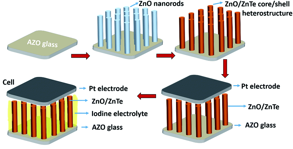 | ||
| Fig. 1 Process flow of preparing the vertically aligned ZnO/ZnTe heterostructure based solar cell. There is a transparent hot-melt ring between Pt counter electrode and ZnO/ZnTe based photoanode. | ||
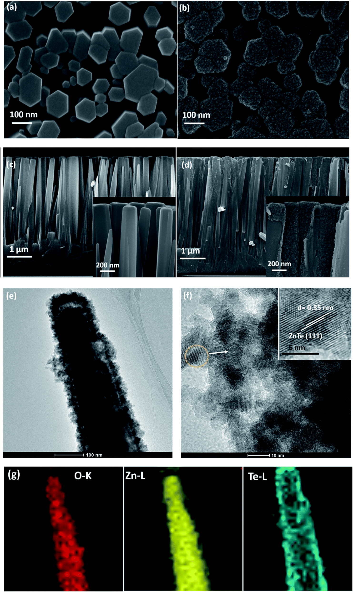 | ||
| Fig. 2 Surface and cross-sectional SEM images of ZnO nanorods (a) and (c) and ZnO/ZnTe heterostructures (b) and (d). Insets of (c) and (d) show the ultra-high magnification SEM images. TEM images of ZnO/ZnTe heterostructure (e) and ZnTe nanoparticles (f). Inset of (f) is a typical HRTEM image of ZnTe nanoparticles. (g) O, Zn and Te elemental EDS mappings for ZnO/ZnTe heterostructure shown in (e), respectively. | ||
As prepared samples were characterized by X-ray diffraction (XRD) and Raman spectroscopy to obtain information on the crystal structure, phase composition and vibrational properties. Here ZnTe nanocrystals were prepared to study the properties of ZnTe alone by prolonging the growth process until the sacrificial ZnO template has been completely removed. Fig. 3 shows the XRD patterns of the AZO-coated glass substrate, ZnO nanorods, ZnTe nanoparticles, and the ZnO/ZnTe heterostructure on the AZO substrate. The diffraction peaks at around 30.9°, 34.4° are attributed to the diffraction from the (1 0 ![[1 with combining macron]](https://www.rsc.org/images/entities/char_0031_0304.gif) 0), (0 0 2) planes of ZnO, which is indexed with the standard diffraction pattern (PDF# 21-1486) and (PDF# 36-1451) with wurtzite-hexagonal crystal structure. Peaks at around 25.3°, 41.8° and 49.5° are ascribed to the diffraction from the (1 1 1), (2 2 0) and (3 1 1) planes of ZnTe, which agrees well with the standard diffraction pattern (JPCDS PDF# 15-0746, cubic structure). On the other hand, the interplanar spacing of ZnTe (1 1 1) plane matches well with the fringe spacing of ∼0.35 nm in Fig. 2(f). With the growth of ZnTe, the peak intensity from ZnO was reduced, due to that the fact that ZnO acted as a sacrificial template for ZnTe. It is noted that the characteristic peaks for ZnO completely disappeared in ZnTe films as compared to the bare ZnO film and ZnO/ZnTe film, indicating that the ZnO nanorods were etched away. This could also be further confirmed by Raman spectra (as shown in Fig. 3(d)). Different scattering intensities at 276 cm−1, 438 cm−1, 580 cm−1 are assigned to the additional mode, high frequency branch of E2 mode and A1 longitudinal optical mode of ZnO, respectively, indicating the wurtzite crystal structure of ZnO.16 The sharp and strong peaks at 125 cm−1, 145 cm−1 are attribute to transverse acoustic mode of ZnTe, while the strong peak at 203 cm−1, along with a weak peak at 410 cm−1 results from the longitudinal optical mode of ZnTe.17 Similar to the results of XRD patterns, the ZnTe film only exhibits Raman peaks from ZnTe, indicating no residual ZnO is existing, which makes it possible to study the properties of ZnTe alone.
0), (0 0 2) planes of ZnO, which is indexed with the standard diffraction pattern (PDF# 21-1486) and (PDF# 36-1451) with wurtzite-hexagonal crystal structure. Peaks at around 25.3°, 41.8° and 49.5° are ascribed to the diffraction from the (1 1 1), (2 2 0) and (3 1 1) planes of ZnTe, which agrees well with the standard diffraction pattern (JPCDS PDF# 15-0746, cubic structure). On the other hand, the interplanar spacing of ZnTe (1 1 1) plane matches well with the fringe spacing of ∼0.35 nm in Fig. 2(f). With the growth of ZnTe, the peak intensity from ZnO was reduced, due to that the fact that ZnO acted as a sacrificial template for ZnTe. It is noted that the characteristic peaks for ZnO completely disappeared in ZnTe films as compared to the bare ZnO film and ZnO/ZnTe film, indicating that the ZnO nanorods were etched away. This could also be further confirmed by Raman spectra (as shown in Fig. 3(d)). Different scattering intensities at 276 cm−1, 438 cm−1, 580 cm−1 are assigned to the additional mode, high frequency branch of E2 mode and A1 longitudinal optical mode of ZnO, respectively, indicating the wurtzite crystal structure of ZnO.16 The sharp and strong peaks at 125 cm−1, 145 cm−1 are attribute to transverse acoustic mode of ZnTe, while the strong peak at 203 cm−1, along with a weak peak at 410 cm−1 results from the longitudinal optical mode of ZnTe.17 Similar to the results of XRD patterns, the ZnTe film only exhibits Raman peaks from ZnTe, indicating no residual ZnO is existing, which makes it possible to study the properties of ZnTe alone.
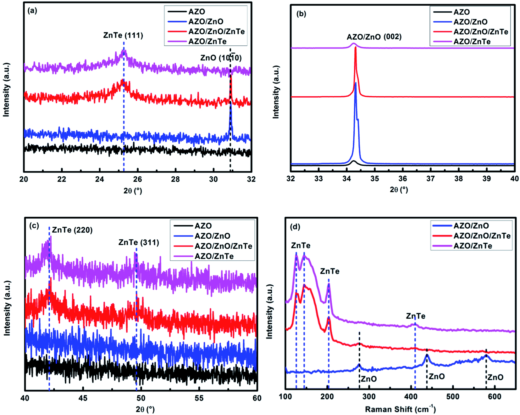 | ||
| Fig. 3 (a–c) XRD patterns of AZO-coated glass substrate, ZnO nanorods, ZnTe nanoparticles and ZnO/ZnTe heterostructure on AZO substrate. (d) Raman spectra of ZnO, ZnTe and ZnO/ZnTe on AZO substrate. | ||
To understand the charge transfer processes between ZnO and ZnTe, PL spectra of ZnO nanorods, ZnTe nanocrystals alone, ZnO/ZnTe heterostructure were measured, as shown in Fig. 4. For comparison, PL spectra of AZO glass, remaining ZnO and the PL intensity for numerical sum of remaining ZnO with ZnTe were also displayed. ZnO nanorods exhibit two emitting bands, a sharp narrow ultraviolet emission peak at 377 nm along with a broad red emission centered at ∼640 nm, which is similar to our previous observations.10 It is widely known that the emission at 377 nm is attributed to the recombination of free excitons in the near-band-edge of the wide band gap ZnO, while the broad visible luminescence is derived from the recombination of a delocalized electron close to the conduction band with a deeply trapped hole in the single negatively charged interstitial oxygen ion Oi− center.18 It should be noted that for our samples, the emission peak of ZnO in the ultraviolet range is much more intense than that in the visible region, indicating good crystallinity and a low concentration of defects. As for the PL spectrum of ZnTe, a broad response in the range of 500–800 nm, with a peak at 636 nm (1.95 eV) was observed, which should be ascribed to combined effect of ZnTe near band edge emission and the oxygen doping of ZnTe nanocrystals.19 Growth of ZnTe on ZnO remarkably reduced both the luminescence intensity of ZnO (both ultraviolet and visible emission) and that of ZnTe. Though the additional non-radiative recombination channels from structural defects associated with lattice corruption by ZnTe deposition or Te0 atoms at ZnO|ZnTe interface acting as traps, would contribute some reduction of PL intensity. We claim that the significantly eliminated PL intensity is primarily attributed to the efficient charge transfer process occurring between ZnO and ZnTe, due to the band alignment in our structure. Indeed, the band alignment of the two materials is type-II, such that the photogenerated electrons transfer from ZnTe to the conduction band of ZnO and the photogenerated holes transfer from the valence band of ZnO to that of ZnTe. Therefore it can be concluded that the growth of ZnTe on ZnO promotes the separation of photoexcited free carriers towards either the electrolyte or anode. The formation of a type-II heterojunction should be reflected in a high internal quantum efficiency, as indeed shown below.
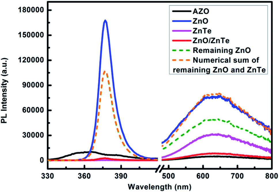 | ||
| Fig. 4 Steady-state PL spectra of AZO glass, ZnO nanorods, ZnTe nanocrystals, ZnO/ZnTe heterostructure. The excitation wavelength of 300 nm was employed to detect the PL properties from 350 nm to 460 nm, and 405 nm was used for the PL properties from 460 nm to 800 nm. When measuring the approximate PL intensity of remaining ZnO nanorods and the numerical sum of remaining ZnO and ZnTe, the thickness of ZnTe layer was considered as ∼20 nm and the diameter of original ZnO nanorod was considered as ∼200 nm (see Fig. 2(e)). | ||
In order to reveal the formation mechanism of ZnO/ZnTe heterostructure, time-dependent reactions were carried out to investigate the growth process. Fig. 5 shows the typical TEM images of the products prepared at certain growth time intervals. It can be observed that the solid ZnO nanorods transformed into a mesoporous arrangement of ZnTe nanocrystals gradually as the reaction progressed. Our strategy for the synthesis of ZnTe nanocrystals is believed to be the result of the Kirkendall effect, which has been employed to synthesize many hollow nanomaterials successfully.20–22 At the initial stage of the growth process, Te2− was adsorbed onto the surface of ZnO nanorods and diffused into the crystal structures by substituting the O atoms out of the rods. This could happen because ZnO shows much larger solubility product (Ksp) than that of ZnTe. Therefore, O atom diffused into the solution much faster than Te atoms, which led to the formation of Kirkendall voids (Fig. 5(c and d)) if the growth time is long enough. As the diffusion reaction proceeded, ZnO/ZnTe heterostructure could be obtained before hollow ZnTe nanocrystals (Fig. 5(e)) came into being, which takes as long as 18 h. The above mentioned process is also called anion exchange, where ZnO acts as sacrificial templates to synthesize ZnTe.
 | ||
| Fig. 5 TEM images of (a) ZnO nanorod and (b–e) ZnO/ZnTe heterostructure with different growth time, (b) 1 h, (c) 2 h, (d) 3 h, (e) 18 h. | ||
As previously reported, the strain between ZnO and ZnTe can affect the band alignment between ZnO and ZnTe. This could depend on the growth method as well as the growth time.9,10 Here, XPS and UV/Vis/NIR measurements were employed to investigate the valence band (VB) and conduction band (CB) positions of ZnTe at different growth times. The optical absorption properties of the various ZnTe samples were used to extract the band gap energy (Eg) of ZnTe nanocrystals. The value of Eg for the ZnO/ZnTe heterostructure was obtained using the equation for the near-edge absorption and the extrapolation of the linear region of the plot of (Ahν)2 against photon energy (hν)23 as shown in Fig. 6(a). Clearly, the Eg of ZnTe decreased with increasing growth time of ZnTe nanocrystals. The extrapolated band gaps were 2.31 eV, 2.28 eV, 2.25 eV, 2.24 eV for growth times of 0.5 h, 1.0 h, 1.5 h, 3.0 h, respectively. This is primarily due to the increased nanocrystal size thus weakened quantum confinement effect. The bandgap is getting closer to its bulk value with the growth time increasing.24,25 Fig. 6(b) shows the valence spectra for the top of the ZnO/ZnTe heterostructure. Based on the work function for the XPS instrument (4.75 eV) and the intersection of baseline with the tangent line of a spectrum, the position of the VB maximum of an electrode can be determined. As in the following, the VB maximum for ZnO/ZnTe with the growth time increasing is estimated to be −5.06 eV, −5.20 eV, −5.12 eV, −5.12 eV relative to vacuum, respectively. This non-monotonous dependence of the VB maximum position among the ZnO/ZnTe photoanodes is a combined effect of strain between ZnO and ZnTe and quantum confinement.9,10 Based on the above analysis, the alignment of energy levels for different ZnO/ZnTe heterostructures can be drawn as shown in Fig. 6(c).
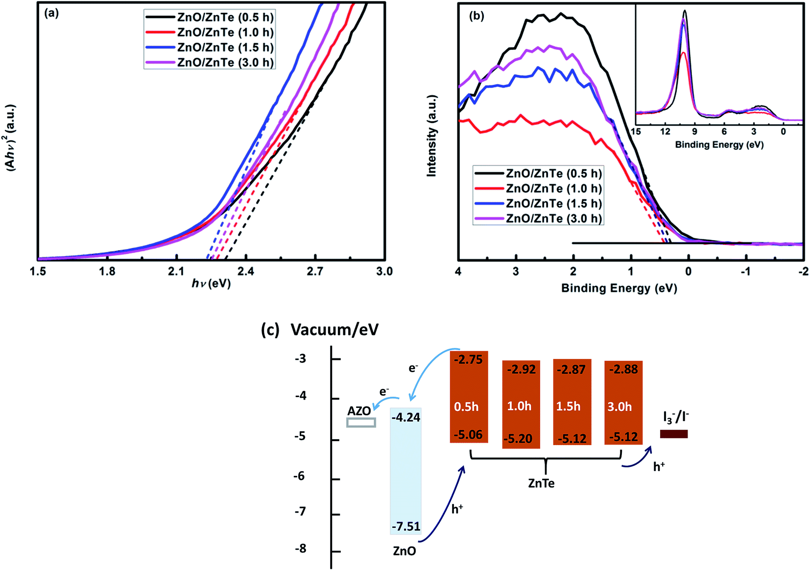 | ||
| Fig. 6 (a) The dependence of (Ahν)2 against photon energy (hν) for ZnO/ZnTe heterostructure using linear extrapolation for the proposed direct forbidden transition. (b) XPS valence spectra and the linear interpolations of the leading edge of ZnO/ZnTe. The inset shows the spectra in wide scan. (c) The band alignment evolution and the corresponding charge transfer process upon illumination in the ZnO/ZnTe heterostructures with different reaction time. | ||
Sensitized solar cells based on ZnO/ZnTe with different ZnTe growth time were fabricated to investigate their photovoltaic performances. The photocurrent density–photovoltage curves (J–V curves) based on different ZnO/ZnTe photoanodes are shown in Fig. 7. Detailed parameters including short-circuit photocurrent density (Jsc), open-circuit photovoltage (Voc), fill factor (FF) and power conversation efficiency (η) are summarized in Table 1. On the whole, ZnO/ZnTe based solar cells possessed high Jsc, which should be attributed to high charge separation efficiency created by the ZnTe–ZnO p–n junction, but with low Voc and FF probably due to charge recombination in the solar cell. By increasing the growth time of ZnTe from 0.5 h to 1 h, notable Jsc and Voc enhancement was observed from 5.14 mA cm−2 to 7.26 mA cm−2 and from 514 mV to 583 mV, respectively. Obviously this result should be on one hand ascribed to the smaller band gap of 1 h-ZnTe than that of 0.5 h-ZnTe due to the reduced degree of quantum confinement. On the other hand, the difference between the CB energy levels of ZnO and ZnTe (1 h) is smaller than that of ZnO/ZnTe (0.5 h), which, while still ensuring a sufficiently large driving force for charge separation results in a reduced energy loss during this process. Nevertheless, further increasing the growth time of ZnTe, the photovoltaic performance decreased as a result of decrease both in Voc and in the FF. When the growth time of ZnTe increased to 3 h, the cell efficiency was further lowered to 0.78%. Apart from the above discussed change in band alignment, the contact between ZnO and ZnTe is gradually modified during growth. In particular, it appears that the system suffers from increased losses which harm its photovoltaic properties. This is further discussed below.
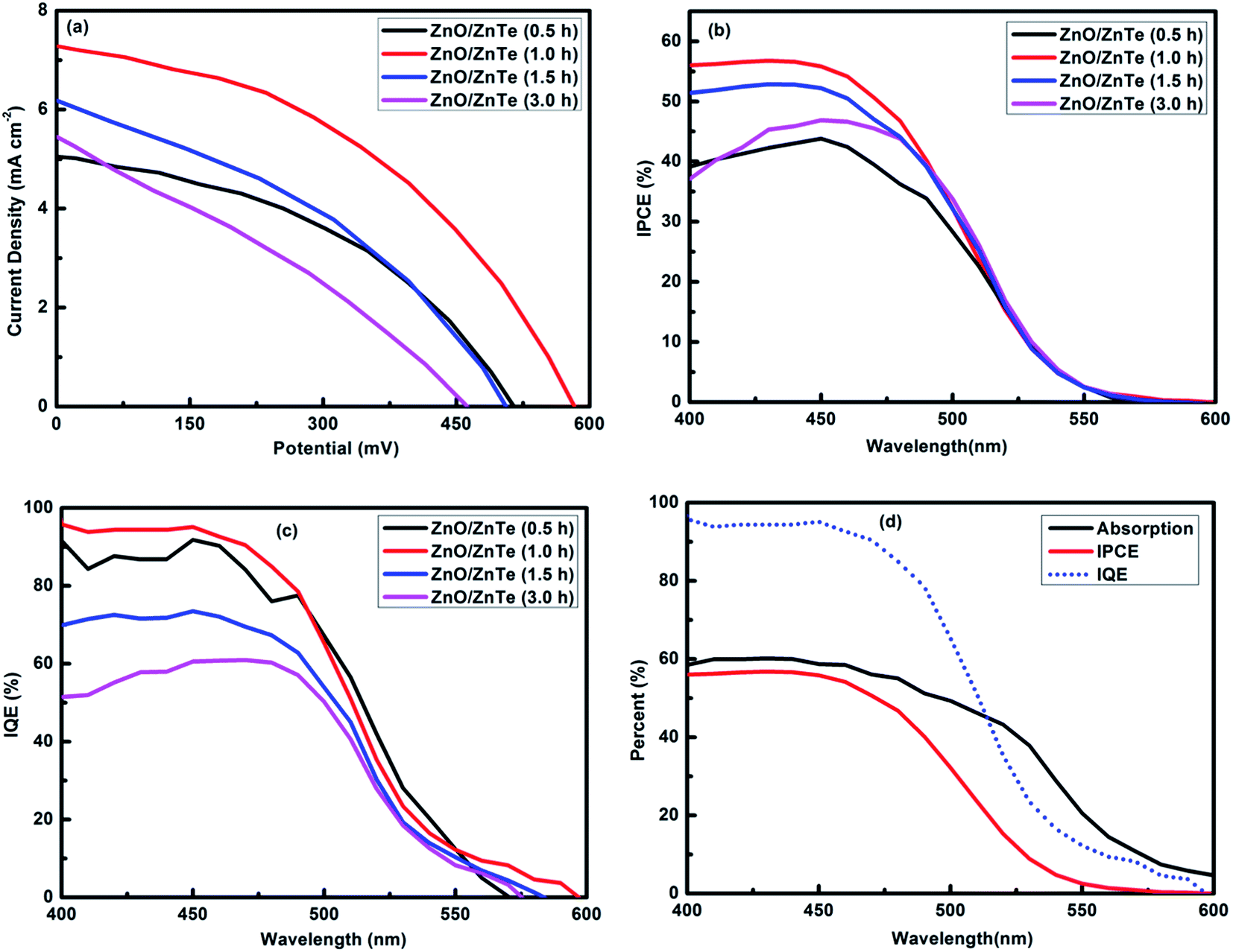 | ||
| Fig. 7 (a) J–V characteristics of solar cells based on ZnO/ZnTe heterostructure with different growth time. IPCE (b) and IQE (c) curves of solar cells based on different ZnO/ZnTe electrodes. (d) Absorption, IPCE and IQE spectra of solar cell based on 1 h-ZnO/ZnTe electrode. | ||
| Photoanode | Jsc (mA cm−2) | Voc (mV) | FF | η (%) |
|---|---|---|---|---|
| ZnO/ZnTe (0.5 h) | 5.14 | 514 | 0.45 | 1.19 |
| ZnO/ZnTe (1.0 h) | 7.26 | 583 | 0.45 | 1.90 |
| ZnO/ZnTe (1.5 h) | 6.21 | 502 | 0.40 | 1.25 |
| ZnO/ZnTe (3.0 h) | 5.43 | 462 | 0.31 | 0.78 |
Measurements of the absorption spectra (Fig. S3†) of ZnO/ZnTe photoanode and the incident monochromatic photon-to-current conversion efficiency (IPCE) spectra (Fig. 7(b)) of the ZnO/ZnTe based solar cells enabled the calculation of the internal quantum efficiency (IQE) spectra shown in Fig. 7(c). Meanwhile, the absorption, IPCE and IQE spectra of solar cell based on 1 h-ZnO/ZnTe electrode are shown together in Fig. 7(d). The IPCE spectra are in good agreement with the trend of Jsc obtained from J–V measurement. It is easily found that solar cell based on 1 h-ZnO/ZnTe possessed remarkably high IQE values, approaching 100%, especially in the range of 400–500 nm. This result indicates that nearly every absorbed photon leads to a separated pair of charge carriers and that almost all carriers photogenerated by wavelengths in this range are collected at the electrodes. The IQE values of all the cells studied here declined rapidly in the wavelength range of 500–600 nm, which is probably attributed to absorption by trap states.
To further clarify charge transport process at the interface of photoanode and counter electrode with the electrolyte, EIS measurements were conducted in the dark. Equivalent circuit model in Fig. 8(c) was employed to further analyze the EIS curves, meanwhile the Nyquist and Bode spectra for different photoanode based solar cells were plotted in Fig. 8(a and b). Two semicircles of the each Nyquist spectrum were observed in the frequency range from 105 Hz to 0.1 Hz in our present study. It is established that the response in the high frequency (leftmost semicircle) can be attributed to the charge transfer at the interface of Pt and electrolyte. The response in the intermediate frequency (right semicircle) corresponds to the charge transfer at the interface of semiconductor and electrolyte. Clearly there is small difference among the leftmost semicircles for all solar cells, as a result of the same counter electrodes and electrolyte. While non-negligible difference among the right semicircles was observed, indicating distinct charge transfer processes at the interface of photoanode and electrolyte. The recombination resistance (Rct) at the ZnO/electrolyte interface could be estimated by the diameter of the second semicircle in the intermediate frequency. Based on the fitting results of the EIS spectra, the Rct was obtained (shown in Table 2). Larger Rct indicates smaller recombination in the solar cells. It is clearly seen that Rct rose firstly and then descended with the increase of ZnTe growth time, and eventually the solar cell based on the 1 h-ZnTe possessed the largest Rct, revealing the smallest recombination. Furthermore, Bode plots of the cells in Fig. 8(b) have been used to estimate the electron lifetime (τn) in the solar cells by the following eqn (1). Longer electron lifetime represents less serious recombination in the complete cell.26
| τn = 1/2πfmin | (1) |
 | ||
| Fig. 8 Nyquist (a) and Bode (b) plots for the solar cells based on ZnO/ZnTe photoanodes with different growth time in the dark at an applied forward bias of −0.7 V. (c) Equivalent circuit for fitting the EIS plots, Rs: series resistance; Rct-CE: charge transfer resistance at the interface of counter electrode (Pt) and electrolyte, Rct-photoanode, recombination resistance at the photoanode/electrolyte interface, CPEct-CE: double-layer capacitance at the counter electrode; CPEct-photoanode: chemical capacitance of ZnO photoanode. | ||
| Photoanode | Rct (Ω cm2) | fmin (Hz) | τn (ms) |
|---|---|---|---|
| ZnO/ZnTe (0.5 h) | 727.8 | 16.98 | 9.38 |
| ZnO/ZnTe (1.0 h) | 818.4 | 11.22 | 14.19 |
| ZnO/ZnTe (1.5 h) | 290.8 | 25.70 | 7.00 |
| ZnO/ZnTe (3.0 h) | 227.4 | 31.62 | 5.04 |
4. Conclusion
In summary, vertically aligned ZnO/ZnTe core/shell heterostructures grown directly from AZO glass with different ZnTe growth times were studied for applications in SSSCs. The details of the type-II energy level alignment between ZnO and ZnTe, which are affected by strain, play an important role on the cell performance. This, in turn, depended on the growth time of ZnTe. When the ZnTe growth time was 1 h, the solar cell achieved the best performance, with a PCE of 1.90%, a Jsc of about 7.26 mA cm−2 and a Voc of 583 mV, IQE values of approaching 100% in a broad range of wavelengths corresponding to band-edge absorption in ZnTe. Considering there is still some space for improvement of Voc, Jsc, and especially the FF, further improvement of the cell performance might be expected by increasing the absorption of the photoanode and constructing more suitable band alignment between ZnO and ZnTe. In this case, there should be large enough driving force with less energy loss for the electrons from ZnTe transferring to ZnO.Acknowledgements
The authors express their gratitude for the support provided by the Ministry of Science & Technology, Israel and the Ministry of Science & Technology, P. R. China: the China-Israel Cooperative Scientific Research Fund (2015DFG52690), and the Joint NSFC-ISF Research Program (51561145007), jointly funded by the National Natural Science Foundation of China and the Israel Science Foundation.References
- S. Mathew, A. Yella, P. Gao, R. Humphry-Baker, F. E. CurchodBasile, N. Ashari-Astani, I. Tavernelli, U. Rothlisberger, K. Nazeeruddin and M. Grätzel, Nat. Chem., 2014, 6, 242–247 CrossRef CAS PubMed
.
- H. Yao, Y. Chen, Y. Qin, R. Yu, Y. Cui, B. Yang, S. Li, K. Zhang and J. Hou, Adv. Mater., 2016, 28, 8283–8287 CrossRef CAS PubMed
- Q. Luo, H. Ma, Y. Zhang, X. Yin, Z. Yao, N. Wang, J. Li, S. Fan, K. Jiang and H. Lin, J. Mater. Chem. A, 2016, 4, 5569–5577 CAS
- D. P. McMeekin, G. Sadoughi, W. Rehman, G. E. Eperon, M. Saliba, M. T. Hörantner, A. Haghighirad, N. Sakai, L. Korte, B. Rech, M. B. Johnston, L. M. Herz and H. J. Snaith, Science, 2016, 351, 151–155 CrossRef CAS PubMed
- X. Lan, O. Voznyy, F. P. García De Arquer, M. Liu, J. Xu, A. H. Proppe, G. Walters, F. Fan, H. Tan, M. Liu, Z. Yang, S. Hoogland and E. H. Sargent, Nano Lett., 2016, 16, 4630–4634 CrossRef CAS PubMed
- S. Luo, H. Shen, Y. Zhang, J. Li, D. Oron and H. Lin, Electrochim. Acta, 2016, 191, 16–22 CrossRef CAS
- B. Zhang, J. Zheng, X. Li, Y. Fang, L. Wang, Y. Lin and F. Pan, Chem. Commun., 2016, 52, 5706–5709 RSC
- J. Wang, Y. Li, Q. Shen, T. Izuishi, Z. Pan, K. Zhao and X. Zhong, J. Mater. Chem. A, 2016, 4, 877–886 CAS
- J. Schrier, D. O. Demchenko and L. W. Wang, Nano Lett., 2007, 7, 2377–2382 CrossRef CAS PubMed
- S. Luo, H. Shen, X. He, Y. Zhang, J. Li, D. Oron and H. Lin, J. Mater. Chem. C, 2016, 4, 4740–4747 RSC
- H. Y. Chao, J. H. Cheng, J. Y. Lu, Y. H. Chang, C. L. Cheng and Y. F. Chen, Superlattices Microstruct., 2010, 47, 160–164 CrossRef CAS
- B. Liu and E. S. Aydil, J. Am. Chem. Soc., 2009, 131, 3985–3990 CrossRef CAS PubMed
- X. Feng, K. Zhu, A. J. Frank, C. A. Grimes and T. E. Mallouk, Angew. Chem., 2012, 124, 2781–2784 CrossRef
- E. Edri, E. Rabinovich, O. Niitsoo, H. Cohen, T. Bendikov and G. Hodes, J. Phys. Chem. C, 2010, 114, 13092–13097 CAS
- M. Kokotov and G. Hodes, J. Mater. Chem., 2009, 19, 3847–3854 RSC
- K. Mahmood, S. B. Park and H. J. Sung, J. Mater. Chem. C, 2013, 1, 3138–3149 RSC
- B. D. McCombe, M. Cardona and R. L. Schmidt, Phys. Rev. B: Condens. Matter Mater. Phys., 1975, 11, 746–753 CrossRef
- X. L. Wu, G. G. Siu, C. L. Fu and H. C. Ong, Appl. Phys. Lett., 2001, 78, 2285–2287 CrossRef CAS
- W. Wang, A. S. Lin and J. D. Phillips, Appl. Phys. Lett., 2009, 95, 011103 CrossRef
- Y. Yin, R. M. Rioux, C. K. Erdonmez, S. Hughes, G. A. Somorjai and A. P. Alivisatos, Science, 2004, 304, 711–714 CrossRef CAS PubMed
- H. J. Fan, U. Gösele and M. Zacharias, Small, 2007, 3, 1660–1671 CrossRef CAS PubMed
- X. Liang, X. Wang, Y. Zhuang, B. Xu, S. Kuang and Y. Li, J. Am. Chem. Soc., 2008, 130, 2736–2737 CrossRef CAS PubMed
- A. Hagfeldt and M. Graetzel, Chem. Rev., 1995, 95, 49–68 CrossRef CAS
- H. J. Yun, T. Paik, B. Diroll, M. E. Edley, J. B. Baxter and C. B. Murray, ACS Appl. Mater. Interfaces, 2016, 8, 14692–14700 CAS
- E. M. Miller, D. M. Kroupa, J. Zhang, P. Schulz, A. R. Marshall, A. Kahn, S. Lany, J. M. Luther, M. C. Beard, C. L. Perkins and J. van de Lagemaat, ACS Nano, 2016, 10, 3302–3311 CrossRef CAS PubMed
- D. Kuang, S. Uchida, R. Humphry-Baker, S. M. Zakeeruddin and M. Grätzel, Angew. Chem., Int. Ed., 2008, 47, 1923–1927 CrossRef CAS PubMed
Footnote |
| † Electronic supplementary information (ESI) available. See DOI: 10.1039/c6ra27641e |
| This journal is © The Royal Society of Chemistry 2017 |