
 Open Access Article
 This Open Access Article is licensed under a
 Creative Commons Attribution 3.0 Unported Licence
Ultra-thin ZnO film as an electron transport layer for realizing the high efficiency of organic solar cells†
Dan Chi *a,
Shihua Huanga,
Shizhong Yueb,
Kong Liub,
Shudi Lub,
Zhijie Wang*b,
Shengchun Qu*b and
Zhanguo Wangb
*a,
Shihua Huanga,
Shizhong Yueb,
Kong Liub,
Shudi Lub,
Zhijie Wang*b,
Shengchun Qu*b and
Zhanguo Wangb
aPhysics Department, Zhejiang Normal University, Zhejiang 321004, China. E-mail: chidan@zjnu.edu.cn
bKey Laboratory of Semiconductor Materials Science, Institute of Semiconductors, Chinese Academy of Sciences, Beijing 100083, People's Republic of China. E-mail: wangzj@semi.ac.cn; qsc@semi.ac.cn
First published on 6th March 2017
Abstract
To overcome the limits of low charge transport efficiency and high absorption in the UV region of conventional thick ZnO layers in organic solar cells, herein we introduce an ultra-thin ZnO film (4 nm) into PBDTTT-CF:PC70BM bulk heterojunction organic solar cells, as the electron transport layer, and realize a power conversion efficiency of 7.51%, which is dramatically higher than that of a device using general ZnO film (28.1 nm). Various techniques from both steady-state and ultra-fast views reveal that the devices with an ultra-thin ZnO film (less than 10 nm) show a higher built-in potential compared to the device with a 28.1 nm ZnO film. Such an enhancement of the built-in potential could facilitate the photo-generated excitons dissociating into free charge carriers and benefit the transport of charge carriers to the electrode. Thus, we have supplied an efficient electron conducting layer not only for the photovoltaic community but also for other photoelectronic devices.
Introduction
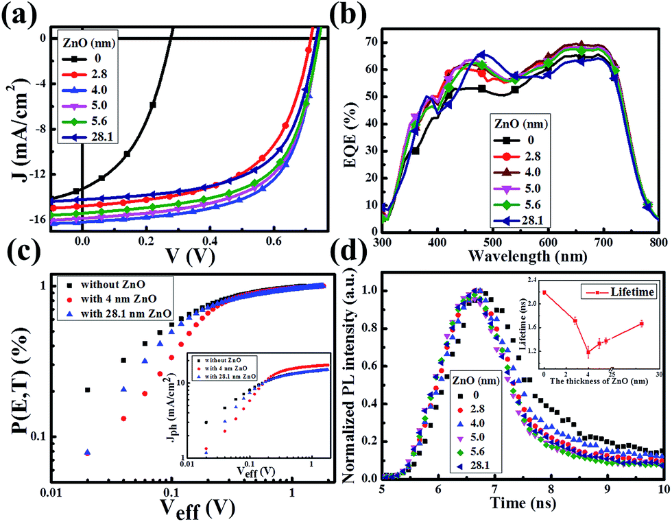
Owing to the great advantages of regulating the work function of an electrode and improving the charge carrier injection and extraction, buffer layers have been extensively utilized in organic-based thin-film optoelectronic devices, including organic solar cells (OSCs), organic light-emitting diodes (OLEDs) and perovskite solar cells (PSCs).1–6 In buffer layers, titanium oxide (TiOx), zinc oxide (ZnO) and cesium carbonate (Cs2CO3) have been incorporated into optoelectronic devices frequently as an electron transport layer and can improve the device performance effectively.7–10 In particular, ZnO is a promising candidate due to its relatively high electron mobility, environmental stability, and transmissivity in the visible region.11–19 There are already plenty of studies about ZnO use in organic solar cells, such as ZnO nanowires, ZnO nanorods, ZnO nanoparticles and ZnO films,15–18 which are all good for the device performance. In a previous study, K. Kim et al. increased the power conversion efficiency (PCE) of OSCs from 7.66% to 7.96% by atomic layer deposition of ZnO film.12 S. Cowan and his coworkers improved the performance of OSCs to 5.93% by modifying the surface of ZnO film.13 Furthermore, W. Qiu et al. improved the PCE of PSCs by using PCBM/ZnO as a double electron transport layer.14 Besides the complexity of these methods, the thickness of the ZnO film in the above studies is more than 45 nm, which will suppress the light harvesting of the active layer in the UV region. The thick film would also increase the transport length of the charge carriers, as a result, and enhance the according recombination possibilities.In light of these issues, we propose a solution process to fabricate an ultra-thin ZnO film, which offers an excellent platform for optimizing the performance of the OSCs without sacrificing the light absorption efficiency. In this work, ZnO films with various thicknesses in the range of 0 to 28.1 nm were introduced in the OSCs, and the device with 4 nm ZnO showed the highest PCE of 7.51%, much higher than that of the reference device with a conventional ZnO film (6.33%). We observe that the dramatically improved PCE is mainly due to an increase of 0.5% in VOC, 13.9% in JSC and 3.6% in fill factor (FF). Further experimental investigations show that the ZnO film improves the device performance by the following aspects: enhancing the built-in potential (Vbi) of the device and increasing the shunt resistance of the system by facilitating the exciton dissociation efficiency and reducing the charge carrier recombination in the ZnO film.
Results and discussion
The solution-processed ultra-thin ZnO films were produced using a carbon free aqueous Zn(OH)x(NH3)y(2−x)+ solution,20–23 and the thicknesses were gauged as 2.8, 4.0, 5.0 and 5.6 nm with the ZnO concentration increasing from 0.04 mol L−1 to 0.07 mol L−1, which are measured by TEM in ref. 22. The 28.1 nm thick ZnO film was fabricated using conventional zinc acetate dehydrate precursor solution.8 Fig. 1a shows the transmittance spectra of the as-prepared ZnO films on quartz glass. In order to make a better comparison, the absorption of the quartz glass has been dubbed out. The ultra-thin ZnO films present high light transmissivity. The transmittance of the ZnO films is in excess of 99% from 350 nm to 800 nm and decreases slightly with the increase of the ZnO thickness. However, the light transmissivity of the thick ZnO film is lower than those of the ultra-thin ZnO films in the range of 200 nm to 800 nm, which could suppress the light absorption efficiency of the active layer in the constructed OSCs. Fig. 1b shows the ultraviolet photoelectron spectroscopy (UPS) spectra of ITO and ZnO films on ITO glass (ZnO–ITO) with different thicknesses. The work function (WF) value can be calculated from the secondary electron cutoff region of the five samples. The value of ITO is 4.4 eV, while those of the ultra-thin ZnO–ITO and 28.1 nm ZnO–ITO are 3.7 eV and 4.1 eV. Obviously, the WF values of ultra-thin ZnO–ITO and 28.1 nm ZnO–ITO are moved upwards by 0.7 eV and 0.3 eV in regard to the pristine ITO, respectively. The low WF values of ZnO–ITO could make the material form good ohmic contact with the active layer. As is known, VOC is mostly affected by the difference between the highest occupied molecular orbital (HOMO) of the donor materials and the lowest unoccupied molecular orbital (LUMO) of the acceptor materials and the WF difference between the cathode and anode.24–27 Theoretically, the larger the WF difference the electrodes have, the larger the VOC presented by the OSCs. Moreover, the lower WF of the ultra-thin ZnO–ITO can increase the Vbi of the devices, which can be beneficial to improve the charge carrier extraction efficiency and reduce the recombination losses. As revealed by the UPS spectra, the thickness of the ultra-thin ZnO has no effect on the WF of ZnO–ITO, which is mainly affected by the synthesis approach. To be significant, the lower WFs of the ultra-thin ZnO compared to the conventional ZnO film make it superior.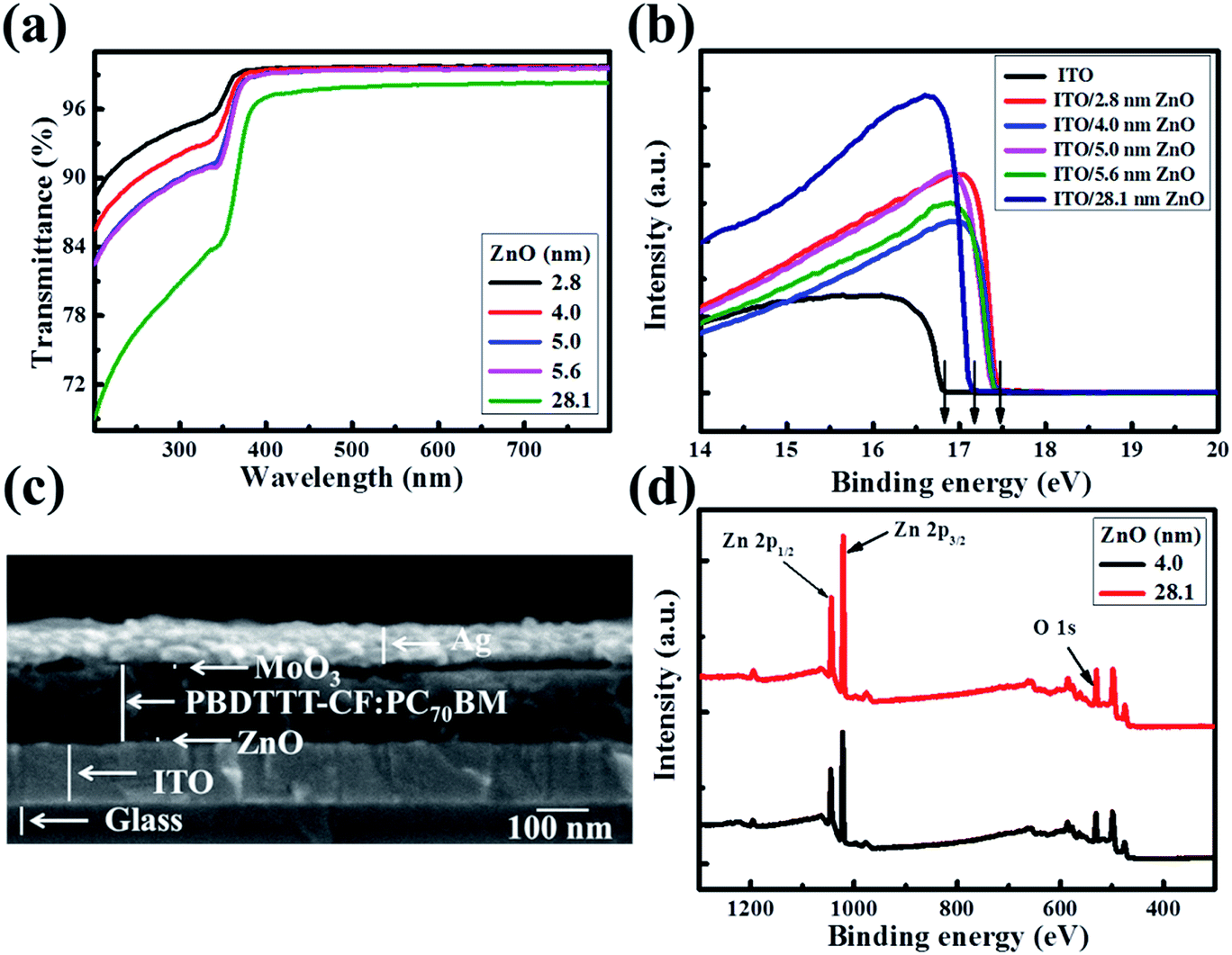 | ||
| Fig. 1 (a) Transmittance spectra of the ZnO films on quartz glass with different thicknesses. (b) UPS spectra of ITO and ZnO films with different thicknesses on ITO glass. The spectra show the energy region of the secondary electron cut-off. (c) The cross-sectional scanning electron microscopy image of the device with a structure of ITO/ultra-thin ZnO/PBDTTT-CF:PC70BM/MoO3/Ag by 0° titled view. (d) X-ray photoelectron spectroscopy (XPS) spectra for Zn 2p1/2, Zn 2p3/2 and O 1s. | ||
Fig. 1c displays the cross-sectional scanning electron microscopy (SEM) image of the device with a structure of ITO/ultra-thin ZnO/PBDTTT-CF:PC70BM/MoO3/Ag by 0° titled view. It can be clearly seen that the ZnO film is ultra-thin. Such a structure could reduce the inefficient light blocking by the ZnO layer, because of the fact that the incident light is from the ITO direction. The MoO3/Ag layer facilitates the hole collection and the ZnO layer is applied for harvesting the electrons generated in the active layer. As exhibited in Fig. S1,† we can see that the ultra-thin ZnO film is very smooth. The smoothness of the ZnO film, which helps to generate good interfacial contact between the cathode and active layer, can decrease the interfacial traps. Therefore, the electron transporting into the interface of the ZnO and active layer can be extracted by the ZnO layer and collected by the cathode successfully. Fig. 1d presents the X-ray photoelectron spectroscopy (XPS) spectra of the 4.0 nm ultra-thin ZnO film and 28.1 nm ZnO film, which exhibits strong Zn 2p1/2, Zn 2p3/2 and O 1s peaks at around 1045 eV, 1022 eV and 531 eV, respectively. This measurement reveals that the ZnO films have no difference in the material aspect. Moreover, it has been reported that the ultra-thin ZnO film has a highly uniform and polycrystalline nature.22 Due to the advantages of the ultra-thin ZnO film, we utilized it as an electron transport layer to optimize the performance of the OSCs herein, and a device with 28.1 nm ZnO was fabricated as a reference.
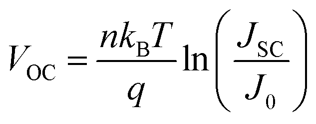
Fig. 2a presents the current density–voltage (J–V) curves of the relevant devices with different thicknesses of the ZnO films under illumination, and the corresponding performance parameters are summarized in Table 1, including the ideality factor (n) and the reverse saturation current density (J0). All the devices with 4 nm to 5.6 nm ultra-thin ZnO film performed better than the device with 28.1 nm thick ZnO film. The OSC works best when the thickness of the ZnO film is 4.0 nm. By introducing 4 nm ZnO into the device and comparing with the conventional device, the VOC, JSC, FF and PCE are prominently enhanced from 0.731 V to 0.735 V, 14.20 mA cm−2 to 16.18 mA cm−2, 61.0% to 63.2% and 6.33% to 7.51%, respectively. The improved properties are mainly due to the enhancement of about 13.9% in JSC. Fig. 2a and Table 1 show that the performances of the devices with 4 nm to 5.6 nm ZnO films are better than those of the devices without ZnO and with 28.1 nm ZnO film. The device parameters with different thicknesses of ZnO film are shown in Fig. S2.† The J–V curves of devices with and without ZnO films under darkness are presented in Fig. S3.† The n and J0, which could characterize the property of the diode, can be extracted from the J–V curves under darkness by fitting the data into the simplified Shockley eqn (1):
 | (1) |
 | ||
| Fig. 2 (a) J–V curves of the devices with different thicknesses of ZnO film under illumination of AM1.5 G, 100 mW cm−2. (b) EQE spectra of the devices with different thicknesses of ZnO film. (c) P[E,T]–Veff curves of the devices without ZnO and with 4 nm and 28.1 nm ZnO film. The inset shows the Jph–Veff curves of the devices without ZnO and with a 4 nm and 28.1 nm ZnO film. (d) Transient PL decays of the structures of ITO/ZnO/PBDTTT-CF:PC70BM with thicknesses of the ZnO film. The inset gives the dependence of the lifetime on the thickness of the ZnO film. | ||
| ZnO (nm) | VOC (V) | JSC (mA cm−2) | FF (%) | PCE(PCEave) (%) | n | J0 (mA cm−2) |
|---|---|---|---|---|---|---|
| 0 | 0.277 | 13.26 | 41.6 | 1.53(1.36) | 1.97 | 6.30 × 10⁻³ |
| 2.8 | 0.713 | 14.75 | 57.3 | 6.02(5.98) | 1.68 | 3.85 × 10⁻⁷ |
| 4.0 | 0.735 | 16.18 | 63.2 | 7.51(7.46) | 1.56 | 6.88 × 10⁻⁸ |
| 5.0 | 0.737 | 15.84 | 61.8 | 7.21(7.14) | 1.59 | 8.18 × 10⁻⁸ |
| 5.6 | 0.739 | 15.39 | 61.4 | 6.98(6.88) | 1.64 | 2.47 × 10⁻⁷ |
| 28.1 | 0.731 | 14.20 | 61.0 | 6.33(6.27) | 1.67 | 1.57 × 10⁻⁷ |
The approach of extracting the parameters has been detailed previously.28–31 As revealed in Table 1, the J0 decreases about 1 order of magnitude from the device with 28.1 nm ZnO to the device with 4 nm ultra-thin ZnO. Therefore the VOC is distinctly improved according to the simplified Shockley equation. The reduced J0 together with the reduced n implies that the ultra-thin ZnO film could inhibit charge carrier recombination, thus suppressing the photogenerated charge carrier loss. Obviously, all the devices with a ZnO film perform better than the device without ZnO (Table 1). This could be proved by the increased external quantum efficiency (EQE) spectra shown in Fig. 2b. The EQE values of the devices with ultra-thin ZnO films are higher than that of the device with a 28.1 nm ZnO film in the range from 550 nm to 800 nm and that of the device without ZnO film in the whole scanned wavelength range, which is consistent with the information in Fig. 2a and Table 1. Fig. 1a shows that the thick ZnO film absorbs more light from 300 nm to 800 nm compared with the ultra-thin ZnO films, especially in the range from 300 nm to 500 nm. Therefore, the device fabricated with a thick ZnO film will impede the absorption of the active layer and reduce the EQE of the device in the range from 300 nm to 500 nm. As a result, the peak in the EQE spectrum of the device with a thick ZnO film shifts toward longer wavelengths and the migration distance is about 25 nm. As demonstrated in Table 1, the ultra-thin ZnO films with thicknesses from 2.8 nm to 5.6 nm show an improved FF of the OSCs.
In order to further investigate the influence of an ultra-thin ZnO film on the exciton generation and dissociation, the maximum exciton generation rate (Gmax) and exciton dissociation probability (P[E,T]) of the device are particularly extracted based on the method previously reported.32–35 Fig. 2c displays the dependence of P[E,T] on the effective voltage (Veff) of the devices with a 4 nm and 28.1 nm ZnO film and the device without a ZnO film. The inset shows the dependence of the photocurrent density (Jph) of these three devices on Veff. Herein, Jph is described by Jph = JL − JD, where JL and JD are the current densities under illumination and under darkness, respectively. Veff is given by Veff = V0 − Va, where V0 is the voltage when Jph is equal to 0 and Va is the applied voltage. The value of the saturation photocurrent density Jsat can be directly extracted from the inset, and Gmax could be derived by Jsat = qGmaxL, if we hypothesise that all of the photogenerated excitons are dissociated and contribute to the current at high Veff, where q is the electronic charge and L is the thickness of the active layer. The values of Gmax for the device without ZnO and the devices with 4.0 nm and 28.1 ZnO are 9.02 × 1027 m−3 s−1 (Jsat = 14.58 mA cm−2), 10.72 × 1027 m−3 s−1 (Jsat = 17.31 mA cm−2) and 9.98 × 1027 m−3 s−1 (Jsat = 15.00 mA cm−2), respectively. The evident improvement of Jsat (about 15.4%) implies that an ultra-thin ZnO film is more beneficial to the transport of the charge carriers, and it is impressively larger than that of the 28.1 nm thick ZnO film, therefore facilitating the enhancement of JSC. As revealed by Fig. 2c, the exciton dissociation probability can be described as Jph = qGmaxP[E,T]L. Thus, the relevant values of P[E,T] at any Veff could be obtained by the normalized current density Jph/Jsat. It is calculated that the values of P[E,T] increased from 80.4% for the device without ZnO to 95.1% and 93.0% for the devices with the 4.0 nm and 28.1 nm ZnO films, which demonstrates that an ultra-thin ZnO film could facilitate the photogenerated excitons to dissociate into free charge carriers efficiently.
To further explore the influence of the ZnO film on exciton dissociation experimentally, we performed transient photoluminescence (PL) measurements for these devices. As shown in Fig. 2d, the samples with an ultra-thin ZnO film present a faster decay in comparison with the sample with a 28.1 nm thick ZnO film, which demonstrates that the ultra-thin ZnO film promotes the separation of the photogenerated excitons. For analyzing these results in more detail, we fit the decay curves using a bi-exponential model. The calculated lifetimes are 2.19 ns (without ZnO), 1.72 ns (2.8 nm ZnO), 1.18 ns (4.0 nm ZnO), 1.33 ns (5.0 nm ZnO), 1.37 ns (5.6 nm ZnO) and 1.67 ns (28.1 nm ZnO). The lifetime as a function of the ZnO film thickness is displayed as the inset in Fig. 2d. It could be noted that the tendency of the transient PL lifetime vs. ZnO film thickness matches well with the trend in the analysis of P[E,T].
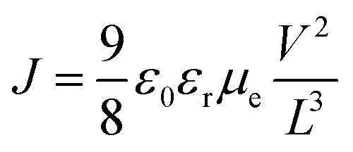
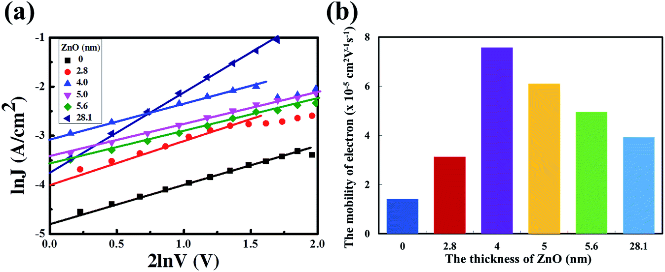
In order to investigate the functionality of the ZnO film, the device with a structure of ITO/ZnO/PBDTTT-CF:PC70BM/Ca/Al was fabricated and the electron mobility is calculated from the space charge limited current (SCLC) method according to eqn (2):
 | (2) |
![[thin space (1/6-em)]](https://www.rsc.org/images/entities/char_2009.gif) J vs. 2lnV curves are presented in Fig. 3a and the electron mobilities with different thicknesses of the ZnO film are shown in Fig. 3b. The electron mobility could be calculated as 1.41 × 10⁻⁵ cm2 V−1 s−1, 3.13 × 10⁻⁵ cm2 V−1 s−1, 7.58 × 10⁻⁵ cm2 V−1 s−1, 6.10 × 10⁻⁵ cm2 V−1 s−1, 4.96 × 10⁻⁵ cm2 V−1 s−1 and 3.93 × 10⁻⁵ cm2 V−1 s−1. Obviously, the electron mobilities of the devices with a 4 nm to 5.6 nm ultra-thin ZnO film are higher than that of the device with a 28.1 nm thick ZnO film. This is due to the highly uniform and polycrystalline nature of the ultra-thin ZnO film.22 The thick ZnO film (28.1 nm) could increase the transport length of the charge carriers, as a result, and enhance the according recombination possibilities, thus reducing the electron mobility. The lower electron mobility of the device with a 2.8 nm ultra-thin ZnO film could originate from the incomplete coverage of the ZnO film on ITO. The ZnO transistor was fabricated via the same aqueous carbon-free metal oxide precursor route showing an electron mobility of up to 11 cm2 V−1 s−1, which means that the electron mobility in the ultra-thin ZnO film is high enough for the electron transport from the active layer to cathode. The detailed results of the ZnO transistor are shown in ref. 22.
J vs. 2lnV curves are presented in Fig. 3a and the electron mobilities with different thicknesses of the ZnO film are shown in Fig. 3b. The electron mobility could be calculated as 1.41 × 10⁻⁵ cm2 V−1 s−1, 3.13 × 10⁻⁵ cm2 V−1 s−1, 7.58 × 10⁻⁵ cm2 V−1 s−1, 6.10 × 10⁻⁵ cm2 V−1 s−1, 4.96 × 10⁻⁵ cm2 V−1 s−1 and 3.93 × 10⁻⁵ cm2 V−1 s−1. Obviously, the electron mobilities of the devices with a 4 nm to 5.6 nm ultra-thin ZnO film are higher than that of the device with a 28.1 nm thick ZnO film. This is due to the highly uniform and polycrystalline nature of the ultra-thin ZnO film.22 The thick ZnO film (28.1 nm) could increase the transport length of the charge carriers, as a result, and enhance the according recombination possibilities, thus reducing the electron mobility. The lower electron mobility of the device with a 2.8 nm ultra-thin ZnO film could originate from the incomplete coverage of the ZnO film on ITO. The ZnO transistor was fabricated via the same aqueous carbon-free metal oxide precursor route showing an electron mobility of up to 11 cm2 V−1 s−1, which means that the electron mobility in the ultra-thin ZnO film is high enough for the electron transport from the active layer to cathode. The detailed results of the ZnO transistor are shown in ref. 22.
 | ||
| Fig. 3 (a) The lnJ vs. 2lnV curves with different thicknesses of the ZnO film. (b) Electron mobility of devices with different thicknesses of the ZnO film. | ||
Collectively, we have shown that the device with an ultra-thin ZnO film performs better than the device with a conventional ZnO film. To get more information on the charge transfer mechanism of the superior device, impedance spectroscopy was recorded. As revealed by Fig. 4a, all of the spectra present the standard semicircle feature of a Nyquist plot, and the semicircle diameters of the devices with an ultra-thin ZnO film are larger than that of the device without ZnO. When the ZnO thickness is 4 nm, the performance of the device reaches the maximum. To further analyze the spectra, we used a typical equivalent circuit shown in the inset to fit these spectra.36–38 The fitted curves are in good agreement with the measured ones, indicating the correctness of the simulation. In the equivalent circuit, we use R1 to represent the transfer recombination component from the active layer to the MoO3/Ag top electrode and R2 as the transfer recombination component from the active layer to ZnO/ITO. These two are connected with a series resistance (Rs) and the extracted data are given in Table S1.† R1 is invariable with the change in ZnO thickness, owing to the same architecture feature of the active layer and MoO3/Ag electrode in these devices. Rs decreases with the thickening of ZnO and reaches the minimum when the thickness is 4 nm. As we increase the thickness further, Rs begins to increase. This feature matches well with the feature of the device performance, which indicates that reduction of Rs is responsible for the performance improvement, particularly in the FF.33,39–43 The optimized ZnO thickness is beneficial for reducing the charge transfer resistance. Alternatively, R2 shows an increasing feature with the enlargement of the ZnO thickness and reaches the maximum when the thickness is 4 nm. Generally, R2 represents the shunt resistance at the ITO/ZnO/active layer, and a large value of R2 usually shows a lower possibility of charge recombination.44–46 A too thin film of ZnO would have a low ability to conduct the electrons to ITO, due to the imperfect coverage that induces a high recombination possibility at the interface of the ITO/ZnO/active layer. A too thick film of ZnO would have a large recombination possibility in ZnO, owing to the long charge transfer length. The charge transfer recombination could also be monitored by IS under different applied potentials and shows an increasing feature with the bias increasing from 0.1 V to 0.7 V, along with a decreased diameter of the semicircles. This is due to the fact that the density of the charge carriers inside the device increases tremendously under a high positive bias, thus more holes and electrons recombine with each other.
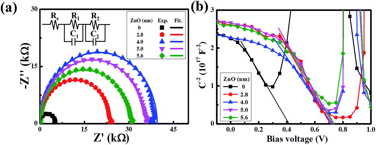 | ||
| Fig. 4 (a) Impedance spectra of the devices with different thicknesses of the ZnO film. (b) Built-in potential (Mott–Schottky plot) of devices with different thicknesses of the ZnO film. | ||
To support the analysis of the improved performance of devices with a ZnO film, we calculated the Vbi of the devices with different ZnO thicknesses from the Mott–Schottky analysis (Fig. 4b). According to eqn (3), we can estimate the Vbi using the following equation:45
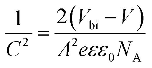 | (3) |
We have also fabricated OSCs with P3HT using a thick ZnO layer and 4 nm ZnO layer. The PCEs of P3HT:PC60BM fabricated using a thick ZnO layer and 4 nm ZnO layer as the electron transport layer are 2.22% and 2.63%, respectively. The J–V curves are shown in Fig. S6.† It can be demonstrated from the J–V curves that the device of P3HT:PC60BM with the ultra-thin ZnO film works better than that with the thick ZnO film. Therefore, the ultra-thin ZnO film can work well as the electron transport layer for P3HT.
Conclusion
In summary, a highly efficient PBDTTT-CF:PC70BM solar cell incorporated with an ultra-thin ZnO film has been fabricated. The ultra-thin ZnO film can improve the device performance in the following aspects: improving the built-in potential of the device by adjusting the work function of ITO; facilitating the exciton dissociation; promoting the charge carrier transportation; reducing the shunt resistance of the device. Therefore, an impressive enhancement in VOC and JSC has been achieved. The maximum PCE of 7.51% is attained for the device with 4.0 nm ZnO. In addition, the proposed carbon free aqueous process for preparing the ultra-thin ZnO is environmentally friendly and could be widely applied in solar cells and LEDs etc.Experimental
Device fabrication
All devices were fabricated on indium tin oxide (ITO) patterned glass substrates, which were cleaned with detergent and sonicated in deionized water, acetone, and then isopropanol for 10 min. Then, the ITO substrates were exposed to O2 plasma for 6 min prior to spin-coating the ZnO thin films at 2000 rpm for 30 s. The precursor solution for fabricating the ultra-thin ZnO films was prepared by dissolving zinc oxide hydrate (ZnO·xH2O, 97%, Sigma-Aldrich) in ammonium hydroxide (28–30%, Sigma-Aldrich) to molar concentrations in the range of 0.04–0.07 M. As-prepared solutions were then stirred rigorously at room temperature for 8 h and became a clear transparent Zn ammonium complex (Zn(OH)x(NH3)y(2−x)+) based solution.20–23 ZnO·xH2O dissolved quickly at a low temperature. Next, the ZnO-coated substrates were annealed at 200 °C for 60 min in air, and then taken into a nitrogen-filled glove box. The active blend layer of PBDTTT-CF (poly[1-(6-{4,8-bis[(2-ethylhexyl)oxy]-6-methylbenzo[1,2-b:4,5-b′]dithiophen-2-yl}-3-fluoro-4-methylthieno[3,4-b]thiophen-2-yl)-1-octanone]):PC70BM ([6,6]-phenyl-C70-butyric acid methyl ester) was spin-coated onto the substrates at 800 rpm for 90 s. The PBDTTT-CF:PC70BM solution consisted of 10 mg ml−1 PBDTTT-CF and 15 mg ml−1 PC70BM in o-dichlorobenzene (ODCB) with 3% 1,8-diiodooctane (1,8-DIO). Finally, a 2 nm MoO3 and 80 nm Ag electrode were evaporated at a base pressure of 9.0 × 10⁻⁵ Pa through a shadow mask. The diameters of oxygen and molybdenum are 0.132 nm and 0.272 nm, respectively. Therefore, the 2 nm MoO3 layer is thick enough to cover the entire surface of the active layer. The ultra-thin MoO3 layer can regulate and control the work function of Ag. The work function of Ag is 4.3 eV which is improper as the anode, while the MoO3 layer with the high work function of 5.4 eV combined with Ag will be perfect as the anode electrode. However, the conductivity of the MoO3 layer is poor. The thick MoO3 layer will reduce the hole extraction rate and thus reduce the device performance. Since the 2 nm MoO3 layer is thick enough to realize good performance for ITO/ZnO/PBDTTT-CF:PC70BM/MoO3/Ag, we just deposited the 2 nm MoO3 layer as the hole transport layer for our organic solar cell.Device measurements
The current density–voltage characteristics of these devices were measured with a computer-controlled Keithley 2400 under AM 1.5 illumination with an intensity of 100 mW cm−2 in a N2 atmosphere (450 W Newport 6279 NS solar simulator). The EQE spectra were collected using Oriel IQE-200™ in air. A He discharge lamp (He I 21.22 eV) was applied to measure the UPS spectra. The XPS measurement (using monochromatized Al Kα X-ray photons, i.e. hν = 1486.6 eV, discharge lamp) was applied to measure the peaks of Zn and O. The IS measurements were performed using a Zahner Zennium electrochemical workstation. The impedance spectra were recorded by utilizing an AC signal in a frequency range of 10 Hz to 1 MHz with an oscillation amplitude of 10 mV. The cross-sectional SEM image of the ZnO film was measured using a JSM-7401F. The thicknesses of the active layers were estimated using a Surface Profilometer (Tencor, ALFA-Step 500). The thicknesses of the ZnO films were measured by an ellipsometer. The principle of ellipsometry is as follows: ellipsometry is an optical technique for investigating the dielectric properties (complex refractive index or dielectric function) of thin films. Ellipsometry measures the change of the polarization upon reflection or transmission and compares it to a model. The measured signal is the change in polarization as the incident radiation interacts with the material structure of interest. The polarization change is quantified by the amplitude ratio (Ψ) and the phase difference (Δ). Upon the analysis of the change of the polarization of light, ellipsometry can yield information about layers that are thinner than the wavelength of the probing light itself, even down to a single atomic layer. Therefore, it can be used to characterize the thickness of the ultra-thin film, and it is very sensitive to the thickness of the material being investigated. In our experiment, the ZnO film is ultra-thin, so we use the Cauchy dispersion equation, which is a suitable model for fitting the data of the transparent thin film, to fit the data collected by the ellipsometer. The Cauchy dispersion equation is shown here: . The A parameter relates to the approximate amplitude for the material index, while the B and C parameters provide the shape or curvature of the index versus the wavelength.
Acknowledgements
This work was mostly supported by the National Basic Research Program of China (Grant No. 2014CB643503), National Natural Science Foundation of China (Contract No. 61504134, 21503209), Beijing Natural Science Foundation (2162042), the Open Project Program of Surface Physics Laboratory (National Key Laboratory) of Fudan University (no. KF2015_02), the Open Project Program of National Laboratory for Infrared Physics, Chinese Academy of Sciences (no. M201503), the Open Project Program of Key Laboratory of Semiconductor Materials Science, Institute of Semiconductors (Chinese Academy of Sciences), Zhejiang Provincial Science and Technology Key Innovation Team (no. 2011R50012), and Zhejiang Provincial Key Laboratory (No. 2013E10022). Z. Wang appreciates the support from the Hundred-Talent Program (Chinese Academy of Sciences).Notes and references
- Z. A. Page, Y. Liu, V. V. Duzhko, T. P. Russell and T. Emrick, Science, 2014, 346, 441 CrossRef CAS PubMed.
- Z. Qi, F. Zhang, C.-a. Di, J. Wang and D. Zhu, J. Mater. Chem. C, 2013, 1, 3072 RSC.
- H. Shen, W. Cao, N. T. Shewmon, C. Yang, L. S. Li and J. Xue, Nano Lett., 2015, 15, 1211 CrossRef CAS PubMed.
- P. Qin, S. Paek, M. I. Dar, N. Pellet, J. Ko, M. Gratzel and M. K. Nazeeruddin, J. Am. Chem. Soc., 2014, 136, 8516 CrossRef CAS PubMed.
- N. Benaziez, A. Ounissi and S. Benaziez, J. Semicond., 2016, 37, 064004 CrossRef.
- Y.-W. Su, S.-C. Lan and K.-H. Wei, Mater. Today, 2012, 15, 554–562 CrossRef CAS.
- X. Dai, C. Shi, Y. Zhang and N. Wu, J. Semicond., 2015, 36, 074003 CrossRef.
- D. Chi, S. Lu, R. Xu, K. Liu, D. Cao, L. Wen, Y. Mi, Z. Wang, Y. Lei, S. Qu and Z. Wang, Nanoscale, 2015, 7, 15251 RSC.
- H. B. Yang, Y. Q. Dong, X. Wang, S. Y. Khoo and B. Liu, ACS Appl. Mater. Interfaces, 2014, 6, 1092 CAS.
- J. Huang, Z. Yin and Q. Zheng, Energy Environ. Sci., 2011, 4, 3861 CAS.
- Y. Sun, J. H. Seo, C. J. Takacs, J. Seifter and A. J. Heeger, Adv. Mater., 2011, 23, 1679 CrossRef CAS PubMed.
- K. D. Kim, D. C. Lim, J. Hu, J. D. Kwon, M. G. Jeong, H. O. Seo, J. Y. Lee, K. Y. Jang, J. H. Lim, K. H. Lee, Y. Jeong, Y. D. Kim and S. Cho, ACS Appl. Mater. Interfaces, 2013, 5, 8718 CAS.
- S. R. Cowan, P. Schulz, A. J. Giordano, A. Garcia, B. A. MacLeod, S. R. Marder, A. Kahn, D. S. Ginley, E. L. Ratcliff and D. C. Olson, Adv. Funct. Mater., 2014, 24, 4671 CrossRef CAS.
- W. Qiu, M. Buffiére, G. Brammertz, U. W. Paetzold, L. Froyen, P. Heremans and D. Cheyns, Org. Electron., 2015, 26, 30 CrossRef CAS.
- J. Jean, S. Chang, P. R. Brown, J. J. Cheng, P. H. Rekemeyer, M. G. Bawendi, S. Gradecak and V. Bulovic, Adv. Mater., 2013, 25, 2790–2796 CrossRef CAS PubMed.
- S. Shoaee, J. Briscoe, J. R. Durrant and S. Dunn, Adv. Mater., 2014, 26, 263–268 CrossRef CAS PubMed.
- P. Zhong, W. Que, Y. N. Liang, X. Yin, Y. Liao, L. B. Kong and X. Hu, RSC Adv., 2013, 3, 17904–17913 RSC.
- S. Alem, J. Lu, R. Movileanu, T. Kololuoma, A. Dadvand and Y. Tao, Org. Electron., 2014, 15, 1035–1042 CrossRef CAS.
- H. C. Chen, S. W. Lin, J. M. Jiang, Y. W. Su and K. H. Wei, ACS Appl. Mater. Interfaces, 2015, 7, 6273–6281 CAS.
- Z. Jin, L. Gao, Q. Zhou and J. Wang, Sci. Rep., 2014, 4, 4268 Search PubMed.
- X. Xu, Q. Cui, Y. Jin and X. Guo, Appl. Phys. Lett., 2012, 101, 222114 CrossRef.
- Y. H. Lin, H. Faber, K. Zhao, Q. Wang, A. Amassian, M. McLachlan and T. D. Anthopoulos, Adv. Mater., 2013, 25, 4340 CrossRef CAS PubMed.
- C.-s. Li, Y.-n. Li, Y.-l. Wu, B.-S. Ong and R.-O. Loutfy, J. Mater. Chem., 2009, 19, 1626 RSC.
- H. Hoppe and N. S. Sariciftci, Adv. Polym. Sci., 2008, 214, 1 CAS.
- H. Hoppe and N. S. Sariciftci, J. Mater. Res., 2004, 19, 1924 CrossRef CAS.
- B. C. Thompson and J. M. Frechet, Angew. Chem., Int. Ed. Engl., 2008, 47, 58 CrossRef CAS PubMed.
- G. Dennler, M. C. Scharber and C. J. Brabec, Adv. Mater., 2009, 21, 1323 CrossRef CAS.
- D. Chi, C. Liu, S. Qu, Z.-G. Zhang, Y. Li, Y. Li, J. Wang and Z. Wang, Synth. Met., 2013, 181, 117 CrossRef CAS.
- B. Qi and J. Wang, J. Mater. Chem., 2012, 22, 24315 RSC.
- K. Vandewal, K. Tvingstedt, A. Gadisa, O. Inganäs and J. V. Manca, Nat. Mater., 2009, 8, 904 CrossRef CAS PubMed.
- W. J. Potscavage, S. Yoo and B. Kippelen, Appl. Phys. Lett., 2008, 93, 193308 CrossRef.
- B. Qi and J. Wang, Phys. Chem. Chem. Phys., 2013, 15, 8972 RSC.
- D. Chi, S. Qu, Z. Wang and J. Wang, J. Mater. Chem. C, 2014, 2, 4383 RSC.
- V. Mihailetchi, L. Koster, J. Hummelen and P. Blom, Phys. Rev. Lett., 2004, 93, 216601 CrossRef CAS PubMed.
- V. D. Mihailetchi, H. X. Xie, B. de Boer, L. J. A. Koster and P. W. M. Blom, Adv. Funct. Mater., 2006, 16, 699 CrossRef CAS.
- F. Tan, S. Qu, Q. Jiang, J. Liu, Z. Wang, F. Li, G. Yue, S. Li, C. Chen, W. Zhang and Z. Wang, Adv. Energy Mater., 2014, 4, 1400512 CrossRef.
- F. Tan, Z. Wang, S. Qu, D. Cao, K. Liu, Q. Jiang, Y. Yang, S. Pang, W. Zhang, Y. Lei and Z. Wang, Nanoscale, 2016, 8, 10198 RSC.
- A. Manjceevan and J. Bandara, Sol. Energy Mater. Sol. Cells, 2016, 147, 157 CrossRef CAS.
- U. Rau, P. O. Grabitz and J. H. Werner, Appl. Phys. Lett., 2004, 85, 6010 CrossRef CAS.
- M. S. Kim, B. G. Kim and J. Kim, ACS Appl. Mater. Interfaces, 2009, 1, 1264 CAS.
- J. Xue, S. Uchida, B. P. Rand and S. R. Forrest, Appl. Phys. Lett., 2004, 84, 3013 CrossRef CAS.
- J. D. Servaites, S. Yeganeh, T. J. Marks and M. A. Ratner, Adv. Funct. Mater., 2010, 20, 97 CrossRef CAS.
- B. Muhsin, J. Renz, K.-H. Drue, G. Gobsch and H. Hoppe, Phys. Status Solidi A, 2009, 206, 2771 CrossRef CAS.
- B. J. Leever, C. A. Bailey, T. J. Marks, M. C. Hersam and M. F. Durstock, Adv. Energy Mater., 2012, 2, 120 CrossRef CAS.
- J. Bisquert, J. Phys. Chem. B, 2002, 106, 325 CrossRef CAS.
- B. Qi, Z. G. Zhang and J. Wang, Sci. Rep., 2015, 5, 7803 CrossRef CAS PubMed.
Footnote |
| † Electronic supplementary information (ESI) available. See DOI: 10.1039/c6ra27543e |
| This journal is © The Royal Society of Chemistry 2017 |