
 Open Access Article
 This Open Access Article is licensed under a Creative Commons Attribution-Non Commercial 3.0 Unported Licence
Morphology-controlled synthesis and electron field emission properties of ZnSe nanowalls
Pei Xieab,
Shaolin Xue *b,
Youya Wangb,
Zhiyong Gaob,
Hange Fengb,
Lingwei Lib,
Dajun Wuc,
Lianwei Wangc and
Paul K. Chud
*b,
Youya Wangb,
Zhiyong Gaob,
Hange Fengb,
Lingwei Lib,
Dajun Wuc,
Lianwei Wangc and
Paul K. Chud
aSchool of Information Science and Technology, Donghua University, Shanghai 201620, China
bCollege of Science, Donghua University, Shanghai 201620, China. E-mail: peipeixie@163.com; slxue@dhu.edu.cn; 15026571630@163.com; gaozhiyong0829@163.com; 17721486315@163.com; li.lingwei.pink@163.com; djwu@ee.ecnu.edu.cn; lwwang@ee.ecnu.edu.cn; paul.chu@cityu.edu.hk; Fax: +86 21 67792089
cKey Laboratory of Polar Materials and Devices, Ministry of Education, and Department of Electronic Engineering, East China Normal University, 500 Dongchuan Road, Shanghai 200241, China
dDepartment of Physics and Material Science, City University of Hong Kong, Tat Chee Avenue, Kowloon, Hong Kong, China
First published on 8th February 2017
Abstract
ZnSe nanowalls are prepared on Zn substrates hydrothermally at 180 °C for 12 h. The structure, morphology, and chemical composition of the ZnSe nanowalls are determined by X-ray diffraction (XRD), scanning electron microscopy (SEM), transmission electron microscopy (TEM), energy-dispersive X-ray analysis (EDS), and Raman scattering. The concentration of hydrazine hydrate (N2H4·H2O) plays an important role in the formation and morphology of the ZnSe nanowalls and XRD reveals that all the ZnSe nanocrystals have a cubic zinc blende structure. The ZnSe nanowalls with an optimal morphology deliver a good field electron emission performance with a turn-on field of 1.51 V μm−1 and enhancement factor of 4797. The formation mechanism is discussed. The simple and controlled preparation procedures and good properties of the ZnSe nanowalls bode well for application in electronics and optoelectronics.
1. Introduction
Two-dimensional (2D) nanomaterials have attracted enormous interest due to their novel and unique characteristics which are different from those of the corresponding bulk materials.1–5 Previous studies have shown that some typical 2D nanomaterials are suitable for potential applications in photodetectors,6 humidity sensors,7 field effect transistors,8 etc. In particular, the field emission properties of 2D nanostructures9–19 have attracted interest due to their potential applications. In field electron emission, electrons are emitted from materials by quantum tunneling through the surface barrier under a strong electric field and the technique is common in high-energy accelerators, flat-panel displays, X-ray sources, microwave amplifiers, and vacuum microelectronic devices. Wang et al.20 reported that carbon nanosheets had a lower turn-on field and higher field enhancement factor than carbon nanorods and Rout et al.21 showed that flower-like VS2 nanosheets had large field enhancement factors due to surface protrusions.Zinc selenide, ZnSe, is an n-type semiconductor with a wide band gap (Eg = 2.67 eV) and used in blue-green light laser diodes,22 blue color light emitting devices,23 gas sensors,24 photo detectors,25 and catalyst supports.26 Hao et al.27 synthesized ZnSe spheres with good photoelectrochemical properties hydrothermally and Zeng et al.28 fabricated ZnSe nanocones and nanobelts on Zn foils and the materials delivered high field emission performance and had good optical characteristics. Zou et al.29 found that the microstructure had a significant effect on the photoluminescence properties of ZnSe nanoribbons and Zannier et al.30 used the vapor–solid–solid (VSS) method to fabricate ZnSe nanowires with a controllable diameter. Morphology-controlled growth of 2D ZnSe nanostructures has been demonstrated and their photovoltaic properties,31 optical properties,32 and photocatalytic properties33 have been investigated.
In this work, 2D ZnSe nanowalls with different morphologies are fabricated on a large scale by a hydrothermal method at 180 °C and the field emission properties are investigated. In the process, the morphology of the ZnSe nanowalls prepared on Zn substrates can be easily controlled by adjusting the concentration of N2H4·H2O so that ZnSe nanowalls with the optimal field emission performance can be obtained. The ZnSe nanomaterials are promising in applications such as field emission displays.
2. Experimental section
2.1 Materials
All the reagents used in this work were analytical grade and used as-received without any purification, including the zinc substrates (Zn) (≥99.0%) (Sinopharm Chemical Reagent Ltd., China), sodium hydroxide (NaOH) (≥97.0%) (Pinghu Chemical Reagent Ltd., China), Se powder (Se) (≥99.7%) (Sinopharm Chemical Reagent Ltd., China), hydrazine hydrate (N2H4·H2O, 85%) (Sinopharm Chemical Reagent Ltd., China), acetone (CH3COCH3) (≥99.7%) (Beijing Chemical Reagent Ltd., China), ethanol (C2H5OH) (≥99.7%) (Beijing Chemical Reagent Ltd., China). The aqueous solutions were prepared with deionized water.2.2 Synthesis of the ZnSe nanowalls
The typical synthesis is described as follows. 0.5 g of Se powder, 65 ml of NaOH (0.24 mol), and 12 ml of N2H4·2H2O were added to a 100 ml beaker under magnetic stirring. After 30 minutes, the Se powder was dissolved to form the solution. The Zn substrate with width of 1 cm, length of 1 cm and thickness of 0.3 mm was utilized also as a reactant. The Zn substrate was ultrasonically cleaned in acetone for 10 min and rinsed with ethanol and deionized water several times was immersed in the solution. The solution with the Zn substrate was put in a 100 ml Teflon-lined stainless steel autoclave and heated to 180 °C in an air-flow electric oven for 12 h. Afterwards, the autoclave cooled naturally to room temperature and the Zn substrate was taken from the solution. Finally, the substrate deposited with ZnSe nanosheets was washed with deionized water and ethanol several times sequentially and dried at room temperature under vacuum before use. ZnSe samples with different morphologies were prepared by changing the concentration of N2H4·2H2O in the solution. The samples obtained using 0, 5, 12, and 14 ml of N2H4·2H2O were termed as Samples 1–4 hereafter for simplicity.2.3 Characterization
The crystal structure and phase composition of the ZnSe nanowalls were determined by X-ray diffraction (XRD; Rigaku-Dmax 2550, Japan) with Cu Kα radiation (λ = 1.5406 Ǻ) at 40 kV and 200 mA in a 2θ range of 20–70°. The composition of the sample was determined by X-ray energy dispersive spectroscope (EDS; Oxford IE 300 X) and the surface morphology was examined by scanning electron microscopy (SEM; JEOL JSM-5600LV), transmission electron microscopy (TEM; Hitachi H-600), and high-resolution transmission electron microscopy (HR-TEM; JEOL JEM-2100). The crystallinity of the ZnSe nanowalls was evaluated by Raman scattering (JY LabRam-1B).2.4 Field emission measurements
The as-prepared sample pasted on polished Al substrate was used as the cathode and the ITO glass was used as the anode. In the measurements, the distance between electrodes was kept ∼500 μm to form a diode structure in the field emission system. Field emission properties of the samples were measured in a ball-type vacuum chamber under a pressure of ∼5 × 10⁻⁴ Pa and the voltage was swept from 0 V up to 3400 V with an interval of 50 V to measure the corresponding field emission current.3. Results and discussion
The XRD spectra of the as-synthesized samples are depicted in Fig. 1 and can be indexed to the cubic zinc blende ZnSe with a = 5.669 Å of the JCPDS file no.80-2346. The diffraction peaks of the ZnSe nanowalls are assigned to the (1 1 1), (2 0 0), (2 2 0), (3 1 1), (2 2 2) and (4 0 0) planes and no characteristic peaks of other crystalline forms are detected by XRD. The composition of the ZnSe nanosheets (Sample 3) determined by EDS indicates that the sample is composed of Zn and Se with a molar ratio of about 1![[thin space (1/6-em)]](https://www.rsc.org/images/entities/char_2009.gif) :1.
:1.
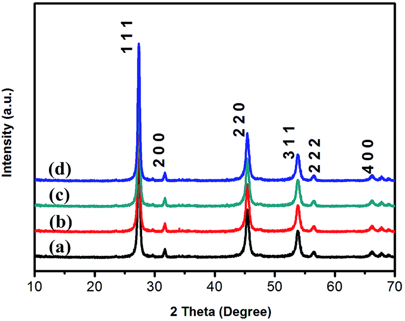 | ||
| Fig. 1 XRD patterns of the ZnSe nanowalls synthetized at 180 °C for 12 h with different concentrations of N2H4·2H2O: (a) Sample 1, (b) Sample 2, (c) Sample 3, and (d) Sample 4. | ||
In order to investigate the influence of the concentration of N2H4·2H2O on the morphology of the ZnSe nanowalls, different experimental procedures are implemented and the products are examined by SEM. Fig. 2(a–d) show the SEM images of 4 ZnSe nanowalls prepared with different concentrations of N2H4·2H2O. As shown in Fig. 2(a), several thick and cluttered wall-like microstructures with the thickness of 60–100 nm are formed without N2H4·2H2O and the nanowalls are distributed irregularly. In the presence of 5 ml N2H4·2H2O, more uniformly distributed and thinner nanowalls are formed, as shown in Fig. 2(b). Fig. 2(b) also shows that the nanowalls with the thickness of approximately 36 nm are thinner than those shown in Fig. 2(a). Fig. 2(c) reveals that the nanowalls are made of thin sheets with the thickness of 20 nm uniformly distributed on the Zn substrate when the amount of N2H4·2H2O is increased to 12 ml. Obviously, the ZnSe nanomaterials shown in Fig. 2(c) have been formed with the thinnest wall compared to Fig. 2(a) and (b). As shown in Fig. 2(d), if the amount of N2H4·2H2O exceeds 12 ml, the thin ZnSe nanowalls with the thickness of approximately 27 nm also uniformly distribute on the Zn substrate but these nanostructures are curlier than those in Fig. 2(c). In addition, the edges of these nanowalls shown in Fig. 2(c) are sharper and the structures are more symmetrical than those of other samples. According to our experimental results, the surface morphology of the ZnSe nanowalls can be controlled by using different concentrations of N2H4·2H2O and the nanostructures with thin and no curly ZnSe nanowalls expected to have the best field emission properties can be produced.
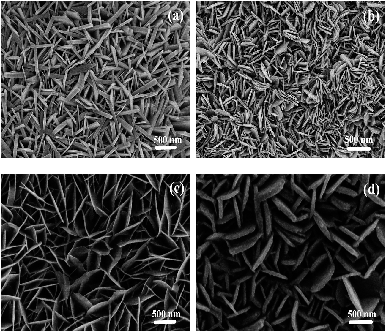 | ||
| Fig. 2 (a–d) SEM images demonstrating the growth of the ZnSe nanowalls at 180 °C for 12 h with N2H4·2H2O (0, 5, 12, and 14 ml, respectively). | ||
In addition, the influence of the different reaction time on the morphology of ZnSe nanowalls (Sample 3) were carried out with other conditions keeping constant. The SEM images obtained at different reaction time are presented in Fig. 3(a–d). When reaction time was performed for 2 h, random and aggregated ZnSe spherical particles were observed, as shown in Fig. 3(a). When the reaction time was continued for 6 h, underdeveloped sphere-like structures evolve into sheet-like structures with small size completely covered the substrate, as shown in Fig. 3(b). As can be seen from Fig. 3(c), when the hydrothermal reaction time was prolonged to 10 h, a large quantity of rough ZnSe nanowalls with large size gradually grow, but there are still some aggregates. Along with the prolonged reaction time (12 h), large-scale regular and uniform nanowalls are formed, as shown in Fig. 2(c).
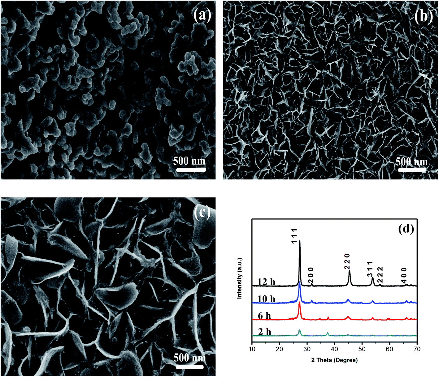 | ||
| Fig. 3 (a–c) SEM images of the as-prepared ZnSe nanowalls under various reaction time: 2 h, 6 h, 10 h, respectively. (d) XRD patterns of the as-prepared ZnSe nanowalls hydrothermally treated for various time. | ||
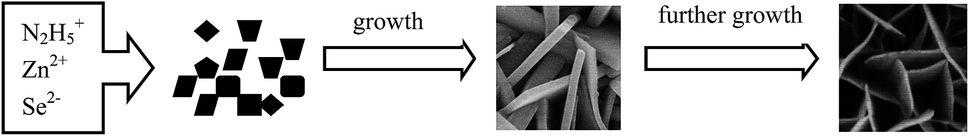
A formation mechanism of ZnSe nanowalls (Sample 3) based on the different reaction time was proposed. Initially, nuclei are formed in the solution and then self-assembled to form small sheet-like structures. As reaction proceeded further, the presence of these assembled nanosheets further develop to form nanowalls with large size. The evolution of the ZnSe nanowalls morphology can be explained by the involvement of Ostwald ripening process. The spontaneously Ostwald ripening in the growth process will decrease the surface free energy of the nanocrystals through increasing the size of nanocrystals, resulting in further growth of superior sheet-like architectures. The results suggest that the generation of nanocrystals with small size is crucial for the formation of nanowalls. Therefore, by controlling the hydrothermal reaction time, the uniform ZnSe nanowalls can be obtained.
The phase structure and composition of the obtained ZnSe nanowalls at different reaction time was investigated by XRD. As can be seen from Fig. 3(d), the XRD patterns of the samples obtained after 2, 6, 10 and 12 h hydrothermal heat treatment show the cubic zinc blende phase. The XRD pattern of the sample prepared by heating for 2 h shows some peaks from impurities such as Se (JCPDS file no. 47-1516). Besides, the intensity of ZnSe peaks are relatively weak indicating poor crystallinity. As the reaction time was prolonged to 6–10 h, the relative intensity diffraction peaks at 37.7° and 60° corresponding to Se become gradually disappeared, whereas the cubic zinc blende phase ZnSe grow rapidly and crystallization becomes better, indicating the formation of ZnSe from selenium. Finally, when the reaction time reached 12 h, ZnSe nanowalls without impurities were obtained. The results of XRD indicate that the crystallinity of ZnSe nanowalls would be enhanced with extended time.
The morphology and structure of the ZnSe nanowalls (Sample 3) are further investigated by TEM, HRTEM and FFT. Fig. 4(a) and (b) show the low-magnification TEM image of an individual nanowall disclosing that it is flat, smooth, and uniform in width. Fig. 4(c) shows the HR-TEM image of the nanowall in Fig. 4(a). The planes with a spacing of about 0.2 nm are parallel to the growth direction coinciding with the interplanar spacing of the cubic ZnSe (2 2 0) planes. Fig. 4(d) displays the corresponding FFT pattern of the nanowall confirming that the hierarchical ZnSe structure is single-crystalline.
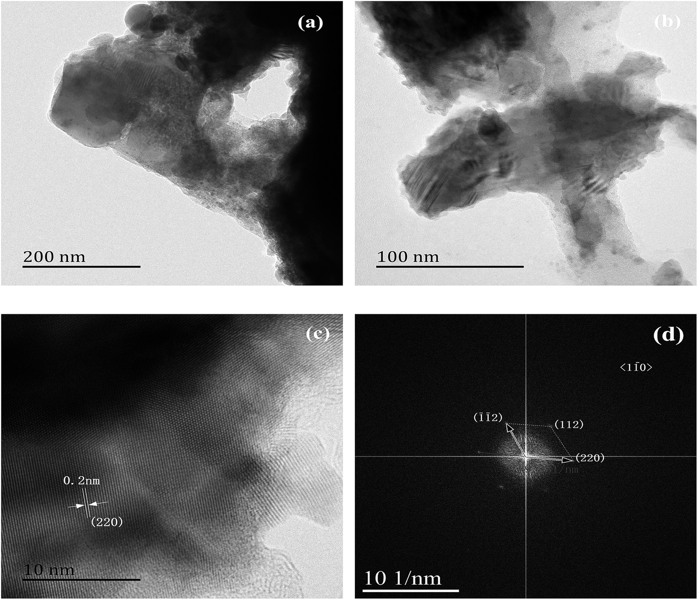 | ||
| Fig. 4 (a) and (b) TEM images of the nanowall, (c) HR-TEM image of the nanowall, and (d) corresponding FFT pattern (Sample 3). | ||
The ZnSe nanowalls are analyzed by Raman scattering34 using the 532 nm excitation wavelength at room temperature. Fig. 5 shows a dominant peak at 251 cm−1 which can be assigned to longitudinal optical (LO) phonon scattering of the ZnSe crystal. The sharp Raman peak indicates that the ZnSe nanowalls have high crystallinity and a pure phase in good agreement with HRTEM and XRD. Compared to the LO phonon scattering peak at 255 cm−1 of previously reported nanocrystalline ZnSe,35 the Raman peak at 250.8 cm−1 shifts to lower frequencies due to the small size and large surface effects.36
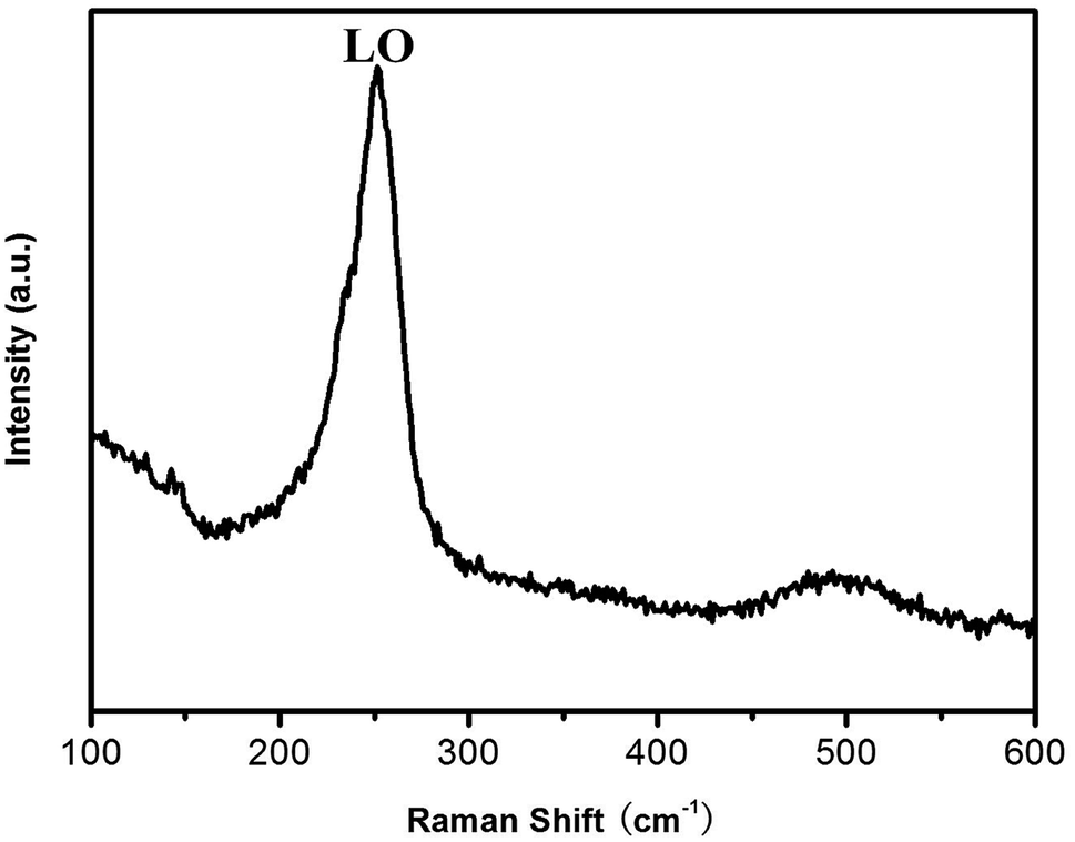 | ||
| Fig. 5 Raman scattering spectrum obtained from the ordered ZnSe nanowalls (Sample 3). | ||
The chemical reactions are shown in the following:
| N2H4·2H2O ⇆ N2H5+ + OH− | (1) |
| N2H5+ + 2Se + 5OH− = N2 + 2Se2− + 5H2O | (2) |
| Zn2+ + 2OH− = Zn(OH)2↓ | (3) |
| Zn(OH)2 + 2OH− = [Zn(OH)2]2− | (4) |
 | ||
| Scheme 1 Formation process of the ZnSe nanowalls. | ||
The FE characteristics are analyzed according to the Fowler–Nordheim (F–N) theory as shown in the following:39
| ln(J/E2) = ln(Aβ2/Φ) − (BΦ3/2/βE), | (5) |
|
ln(J/E2) = lna − b(1/E),
| (6) |
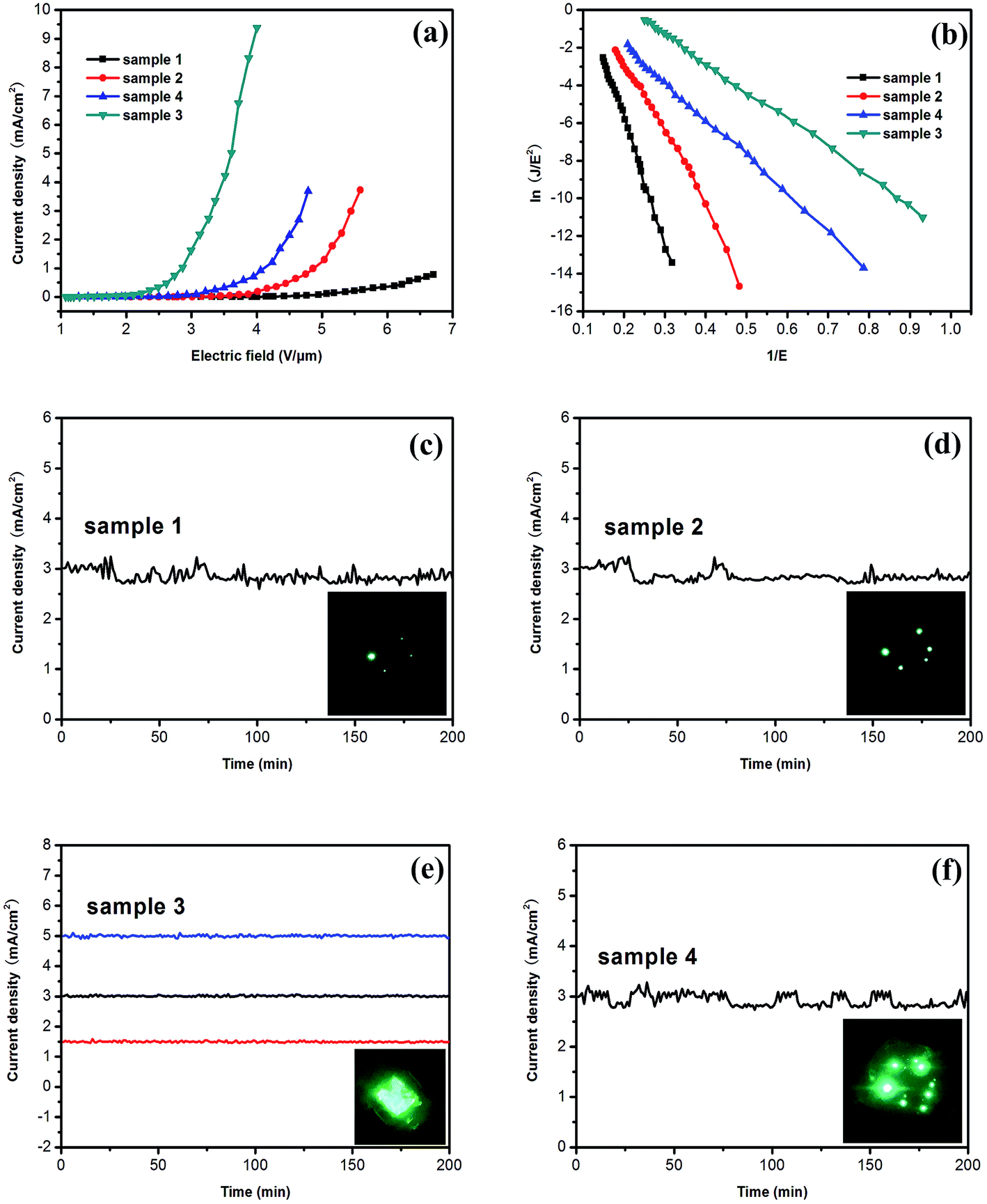 | ||
| Fig. 6 (a) Field emission J–E curve, (b) FN plot, and (c–f) long-term field emission current stability test conducted on samples 1–4 (the insets show the fluorescence field emission image of the corresponding samples). | ||
Fig. 6(b) shows the relationship between ln(J/E2) and 1/E. The F–N plots show a roughly linear relationship implying that quantum tunneling is responsible for the emission. By using the slopes of F–N plot and assuming a work function of 4.84 eV for bulk ZnSe,40 β was calculated to be 1109, 1896, 3678, and 4797 for samples 1, 2, 3, and 4, respectively. The field enhancement factor (β) depends on the areal density and geometry of the emitters. Comparing the four samples with different, the Sample 3 with medium density of emission spots shows higher field enhancement than the Sample 2 with high density of emission spots due to the relatively low density of emitters preventing the electrostatic screening effect.41 The Sample 3 with thin nanowalls exhibits higher emission than the Sample 1 with thick nanowalls due to the structures with thin sheets and sharp edges. Moreover, Sample 3 have sharper edge-like structures than Sample 4 with curly edges thus favoring field emission. All in all, ZnSe nanowalls composed of thin nanosheets (Sample 3) possessing low turn-on field and large enhancement factor may be ascribed to the desired thickness of nanowalls and sharp edges on the surface, as shown in Fig. 2(c). Hence, the enhanced field emission performance can be achieved by adjusting the thickness of ZnSe nanowalls.
Fig. 6(c–f) show the field emission stability of the 4 samples by plotting the emission current density as a function of time. The field-emission current density of 4 samples is monitored for 200 min at an initial emission current density of 3 mA cm−2. Besides, the field emission current density of Sample 3 was monitored at an initial emission current density of 1.5 mA cm−2 and 5 mA cm−2. The result suggests that the overall fluctuations in field emission current of Sample 3 does not show significant degradation indicating excellent emission stability.
Table 1 lists the turn-on fields and field enhancement factors of different ZnSe field emitters reported in the literature and from this work. The FE performance of the ZnSe nanowalls described here are generally comparable to other ZnSe nanostructures such as nanoribbons,40 nanoarrays,42 nanoflowers43 and nanograsses.44
4. Conclusion
High-quality sheet-based ZnSe nanomaterials with controlled morphologies are synthesized hydrothermally. The ZnSe nanowalls are composed of radially aligned ZnSe nanosheets of single-crystal ZnSe nanocrystals with a cubic zinc blende structure. The concentration of hydrazine hydrate plays an important role in the formation of the sheet-based ZnSe nanostructures. The investigation of field emission properties indicated that the ZnSe nanowalls composed of the thin and no curly nanosheets show a low turn-on field of 1.51 V μm−1 and high enhancement factor of 4797. The samples have potential in flat-panel-displays.Acknowledgements
This work was supported by the Natural Science Foundation of China (No. 61072003) and City University of Hong Kong Applied Research Grant (ARG) No. 9667122.References
- A. S. Pawbake, M. S. Pawar, S. R. Jadkar and D. J. Late, Nanoscale, 2016, 8, 3008–3018 RSC.
- K. K. Naik, R. T. Khare, R. V. Gelamo, M. A. More, R. Thapa, D. J. Late and C. S. Rout, Mater. Res. Express, 2015, 2, 095011 CrossRef.
- C. S. Rout, P. D. Joshi, R. V. Kashid, D. S. Joag, M. A. More, A. J. Simbeck, M. Washington, S. K. Nayak and D. J. Late, Sci. Rep., 2013, 3, 3282 Search PubMed.
- S. R. Suryawanshi, A. S. Pawbake, M. S. Pawar, S. R. Jadkar, M. A. More and D. J. Late, Mater. Res. Express, 2016, 3, 035003 CrossRef.
- M. S. Pawar, P. K. Bankar, M. A. More and D. J. Late, RSC Adv., 2015, 5, 88796–88804 RSC.
- M. B. Erande, M. S. Pawar and D. J. Late, ACS Appl. Mater. Interfaces, 2016, 8, 11548–11556 CAS.
- L. D. Bharatula, M. B. Erande, I. S. Mulla, C. S. Rout and D. J. Late, RSC Adv., 2016, 6, 105421–105427 RSC.
- Y. B. Zhu, C. Wang, N. Petrone, J. Yu, C. Nuckolls, J. Hone and Q. Lin, Appl. Phys. Lett., 2015, 106, 123503 CrossRef PubMed.
- D. J. Late, P. A. Shaikh, R. Khare, R. V. Kashid, M. Chaudhary, M. A. More and S. B. Ogale, ACS Appl. Mater. Interfaces, 2014, 6, 15881–15888 CAS.
- M. B. Erande, S. R. Suryawanshi, M. A. More and D. J. Late, Eur. J. Inorg. Chem., 2015, 19, 3102–3107 CrossRef.
- S. R. Suryawanshi, M. A. More and D. J. Late, RSC Adv., 2016, 6, 112103–112108 RSC.
- S. R. Suryawanshi, P. S. Kolhe, C. S. Rout, D. J. Late and M. A. More, Ultramicroscopy, 2015, 149, 51–57 CrossRef CAS PubMed.
- R. Khare, D. B. Shinde, S. Bansode, M. A. More, M. Majumder, V. K. Pillai and D. J. Late, Appl. Phys. Lett., 2015, 106, 023111 CrossRef.
- S. R. Suryawanshi, M. A. More and D. J. Late, J. Vac. Sci. Technol., B: Nanotechnol. Microelectron.: Mater., Process., Meas., Phenom., 2016, 34, 041803 Search PubMed.
- J. Q. Wu, S. Z. Deng, N. S. Xu and J. Chen, Appl. Surf. Sci., 2014, 292, 454–461 CrossRef CAS.
- S. Jana, S. Das, N. S. Das and K. K. Chattopadhyay, Mater. Res. Bull., 2010, 45, 693–698 CrossRef CAS.
- V. C. Anitha, A. N. Banerjee, S. W. Joo and B. K. Min, Nanotechnology, 2015, 26, 355705 CrossRef CAS PubMed.
- X. P. Feng, Y. X. Li, H. B. Liu, Y. L. Li, S. Cui, N. Wang, L. Jiang, X. F. Liu and M. J. Yuan, Nanotechnology, 2007, 18, 145706 CrossRef.
- Y. J. Zhang, H. Li, L. Jiang, H. B. Liu, C. Y. Shu, Y. L. Li and C. R. Wang, Appl. Phys. Lett., 2011, 98, 113118 CrossRef.
- B. B. Wang, K. Ostrikov, T. van der Laan, K. Zheng, J. J. Wang, Y. P. Yan and X. J. Quan, J. Mater. Chem. C, 2013, 1, 7703–7708 RSC.
- C. S. Rout, R. Khare, R. V. Kashid, D. S. Joag, M. A. More, N. A. Lanzillo, M. Washington, S. K. Nayak and D. J. Late, Eur. J. Inorg. Chem., 2014, 31, 5331–5336 CrossRef.
- G. Kiriakidis, K. Moschovis, P. Uusimaa, A. Salokatve, M. Pessa and J. Stoemenos, Thin Solid Films, 2000, 360, 195–204 CrossRef CAS.
- W. Y. Ji, P. T. Jing, W. Xu, X. Yuan, Y. J. Wang, J. L. Zhao and A. K.-Y. Jen, Appl. Phys. Lett., 2013, 103, 053106 CrossRef.
- K. M. Ip, Z. Liu, C. M. Ng and S. K. Hark, Nanotechnology, 2005, 16, 1144–1147 CrossRef CAS.
- X. Gao, G. C. Tang and X. G. Su, Biosens. Bioelectron., 2012, 36, 75–80 CrossRef CAS PubMed.
- T. T. Yao, Q. Zhao, Z. P. Qiao, F. Peng, H. J. Wang, H. Yu, C. Chi and J. Yang, Chem.–Eur. J., 2011, 17, 8663–8670 CrossRef CAS PubMed.
- Y. Z. Hao and Y. Feng, Chem. J. Chin. Univ., 2008, 29, 788–792 CAS.
- Q. Z. Zeng, S. L. Xue, S. X. Wu, K. X. Gan, L. Xu, J. W. Han, W. K. Zhou, Y. T. Shi and R. J. Zou, Mater. Sci. Semicond. Process., 2015, 31, 189–194 CrossRef CAS.
- Y. Q. Zou, H. L. Li, P. Y. Ren, J. Y. Xu, L. Ma, X. X. Wang, X. P. Fan, Z. P. Shan, X. J. Zhuang, H. Zhou, X. L. Zhu, Q. L. Zhang and A. L. Pan, Mater. Lett., 2014, 129, 118–121 CrossRef CAS.
- V. Zannier, V. Grillo and S. Rubini, J. Phys. D: Appl. Phys., 2014, 47, 394005 CrossRef.
- C. Fan, Q. L. Zhang, X. L. Zhu, X. J. Zhuang and A. L. Pan, Sci. Bull., 2015, 60, 1674–1679 CrossRef CAS.
- B. Feng, J. H. Yang, J. Cao, L. L. Yang, M. Gao, M. B. Wei, H. J. Zhai, Y. F. Sun and H. Song, J. Alloys Compd., 2013, 555, 241–245 CrossRef CAS.
- J. J. Yin, G. Y. Feng and S. H. Zhou, J. Optoelectron. Adv. Mater., 2015, 9, 682–687 CAS.
- Q. L. Bao, Y. Gan, J. Li and C. M. Li, J. Phys. Chem. C, 2008, 112, 19718–19726 CAS.
- X. Wang, X. Chen, H. Zheng, J. Jin and Z. Zhang, Appl. Phys. A: Mater. Sci. Process., 2005, 80, 511–513 CrossRef CAS.
- H. Q. Cao, Y. J. Xiao and S. C. Zhang, Nanotechnology, 2011, 22, 015604 CrossRef PubMed.
- Y. J. Dong, Q. Peng and Y. D. Li, Inorg. Chem. Commun., 2004, 7, 370–373 CrossRef CAS.
- L. L. Chai, J. Du, S. L. Xiong, H. B. Li, Y. C. Zhu and Y. T. Qian, J. Phys. Chem. C, 2007, 111, 12658–12662 CAS.
- J. Z. Xu, R. Pan, Y. W. Chen, X. Q. Piao, M. Qian, T. Feng and Z. Sun, J. Alloys Compd., 2013, 551, 348–351 CrossRef CAS.
- L. J. Zhao, Q. Pang, Y. Cai, N. Wang, W. K. Ge, J. N. Wang and S. H. Yang, J. Phys. D: Appl. Phys., 2007, 40, 3587–3591 CrossRef CAS.
- C. X. Wu, F. S. Li, Y. G. Zhang and T. L. Guo, Carbon, 2012, 50, 3622–3626 CrossRef CAS.
- Q. Su, L. J. Li, S. Y. Li and H. P. Zhao, Micro Nano Lett., 2012, 7, 1053–1055 Search PubMed.
- S. L. Xue, S. X. Wu, Q. Z. Zeng, P. Xie, K. X. Gan, J. Wei, S. Y. Bu, X. N. Ye, L. Xie, R. J. Zou, C. M. Zhang and P. F. Zhu, Appl. Surf. Sci., 2016, 365, 69–75 CrossRef CAS.
- W. K. Zhou, S. L. Xue, J. W. Han and P. Xie, Mater. Lett., 2014, 134, 256–258 CrossRef CAS.
| This journal is © The Royal Society of Chemistry 2017 |