
 Open Access Article
 This Open Access Article is licensed under a
 Creative Commons Attribution 3.0 Unported Licence
Influence of removing PMMA residues on surface of CVD graphene using a contact-mode atomic force microscope†
Woosuk Choi,
Muhammad Arslan Shehzad,
Sanghoon Park and
Yongho Seo *
*
Department of Nanotechnology, Advanced Material Engineering, Graphene Research Institute, Sejong University, Seoul, 143-747, Korea. E-mail: yseo@sejong.ac.kr; Tel: +82-2-3408-3689
First published on 20th January 2017
Abstract
For device fabrication based on 2D materials such as graphene, hexagonal boron nitride (hBN) and transition metal dichalcogenides (TMDs), polymethyl methacrylate (PMMA) is conventionally used in the wet transfer and lithography processes. All these processes are sources of polymer residue, which degrade the intrinsic electrical and optical properties of devices. In this work, we report the effect of mechanical cleaning via contact mode atomic force microscopy (AFM) on the surface morphology and electrical behavior of chemical-vapor-deposition grown graphene. An AFM tip with large contact force was used to scan, and multiple scanning was performed to remove the residues of PMMA. Raman mapping was incorporated to confirm the cleaning effect using AFM. Transconductance properties associated with a field-effect-transistor device based on the cleaned graphene were analyzed. It was observed that charge-neutrality point was shifted towards zero gate voltage and the charge carrier mobility was increased. We claim that our technique provides a facile route to fabricate devices with less polymer residue and higher efficiency.
Introduction
Since 2D materials such as graphene,1 hexagonal boron nitride (hBN), and the transition metal dichalcogenides were discovered, there have been many studies on the fabrication of 2D material-based efficient devices for the next generation.2–7 Polymethyl methacrylate (PMMA) is commonly used as a supporting layer, to transfer them into other substrates.8 After transfer, PMMA cannot be removed completely, and the residue of PMMA degrades intrinsic electric and optical properties of 2D materials.9–12 To address this issue, solutions such as annealing,13–17 chemicals,14 current-induced18,19 atomic force microscope (AFM) cleaning,20–23 rubbing cloth to induce electrostatic force,24 inductively coupled plasma,25 stencil mask patterning,26,27 andCO2 cluster28 are usually employed.Each solution can be useful but has its own limitation. Mostly, high temperature annealing in Ar/H2,13,14 N2/H2,15 or vacuum16 is employed to clean the graphene surface. It has been known that the annealing is not the ideal method to completely remove the residue.29 Moreover, due to its high temperature, structural damage deforms graphene which degrades the device performance.14,17 This deformation is due to coupling between the substrate and graphene.14 Cheng et al. suggested a chemical cleaning method using chloroform, but the solvent cannot remove all the residues, and its effect is insufficient compared to the annealing method.14 In order to use the current-induced cleaning, electrodes to induce current should be fabricated. Due to the high current density, this cleaning method may cause burning or ripping of graphene by heat.18,19
The AFM cleaning method20–22 utilizes the mechanical force from AFM, of which advantages include direct removal of polymer residue with no chemical reaction on the surface of graphene. Lindvall et al. cleaned the exfoliated graphene on various substrates such as barium titanium oxide (BTO) and SiO2 by using the AFM cleaning.22 In particular, the height roughness (Rrms) was reduced by 90% on BTO substrate, and the carrier mobility was increased by about 20% on the SiO2 substrate. Goossens et al. used the AFM cleaning combined with annealing methods to clean the exfoliated graphene on hBN substrate.21 Annealing at the temperature range from 360 to 440 °C was performed prior to the mechanical cleaning. As the result, 80% of device mobility was increased. These results indicate that the AFM cleaning could be more effective if it can be combined with other methods.
On the other hand, the chemical-vapor-deposition (CVD) grown graphene films can be synthesized in wafer scale and then processed by standard microfabrication techniques. However, the properties of CVD grown graphene is still poor compared to exfoliated graphene due to intrinsic and extrinsic defects.15,30,31 Many groups have investigated methods to improve the properties of CVD grown graphene,10,32 but the works are still far from satisfactory. Pirkle et al. reported that the cleaning of the residue remaining on the graphene surface in the transfer process caused a significant increment of the mobility.10
In this paper, the AFM cleaning method was applied to CVD grown graphene transferred to SiO2, to improve the electrical properties of CVD graphene. Also, the AFM cleaning can reduce the ripples that might occur in the transfer process.21 The cleaning effect and mechanical damage to the graphene by the AFM cleaning was analyzed by using a Raman spectroscopy mapping system. Also, transconductance properties of the back-gated field effect transistor based on the cleaned graphene were analyzed.
Experiment and method
Single-layer graphene was synthesized by CVD technique on copper foil (25 μm thick, 99.8% purity, Alfa Aesar) at 950 °C and pressure of 1 × 10⁻³ Torr in a silica tube with Ar/H2 mixture gas at the rate of 250/100 sccm was used, and 50 sccm of CH4 was adopted as the carbon source. To transfer the grown graphene from Cu foil to a SiO2/Si wafer, polymethyl methacrylate (PMMA) (950, A2 from MicroChem Inc.) film was spin-coated at a spin speed of 500 rpm for 5 s, followed by 4000 rpm for 40 s on top of the graphene layer to be ∼200 nm thick. The sample was dried under ambient conditions at room temperature for 15 min. As the graphene was grown on both sides of the copper foil, the unneeded back side graphene was etched by oxygen plasma. To remove the copper substrate, the Cu foil was dissolved in 1 M ammonium persulfate ((NH4)2S2O8) solution for one day and rinsed in deionized (DI) water. The standard-clean-2 (SC2) cleaning process (20![[thin space (1/6-em)]](https://www.rsc.org/images/entities/char_2009.gif) :1:1, 15 min at room temperature), DI water rinsing, and SC1 cleaning process were performed sequentially to remove metallic and organic residues. The resulting graphene/PMMA layer was transferred onto a clean Si/SiO2 substrate (300 nm thermal oxide) and baked at 150 °C for 15 min. In order to remove the PMMA layer, the sample was immersed into acetone for a day and rinsed in isopropyl alcohol (IPA).
:1:1, 15 min at room temperature), DI water rinsing, and SC1 cleaning process were performed sequentially to remove metallic and organic residues. The resulting graphene/PMMA layer was transferred onto a clean Si/SiO2 substrate (300 nm thermal oxide) and baked at 150 °C for 15 min. In order to remove the PMMA layer, the sample was immersed into acetone for a day and rinsed in isopropyl alcohol (IPA).
The samples for measurement by Raman spectroscopy were marked by a razor with X-shape in order to spot the area as shown in Fig. 2(a). After the AFM cleaning the surface was investigated by a micro Raman spectroscopy mapping system (Renishaw, InVia systems). The Raman system was equipped with a laser line of 514.5 nm (argon ion) and spectral resolution of 3 cm−1. The laser beam spot size was about 1 μm, and the laser power was set to about 2 mW to minimize laser heating effects. The Raman mapping was measured with a scanner having a spatial resolution of ∼800 nm. An auto-focus function was used in 2 steps to correct the tilt of the sample.
In order to measure electrical properties, a back-gated graphene field-effect-transistor (FET) device was fabricated by using photolithography. A photoresist (AZ GXR-601, Electronics Material, Inc.) was used to make a Hall bar geometry, and O2 plasma was applied for reactive ion etching (RIE). Electron-beam evaporation was used to make electrodes with Ti (1 nm) followed by Au (80 nm) for electrical contacts to the graphene channels (‘source’ and ‘drain’) (see ESI, Fig. S1†). Electrical measurements were performed at room temperature under vacuum conditions before and after the cleaning.
Results and discussion
1. AFM cleaning
To remove the residues of PMMA, the CVD graphene was scanned in contact-mode by a commercial AFM (XE-100 from Park's systems Inc.). To apply a strong force, a stiff cantilever (Multi75DLC, force constant: 3 N m−1) was used, which is 100 times stronger than conventional cantilever for the contact-mode (0.06–0.4 N m−1). The technical parameter of the AFM cleaning is normal force perpendicular to the surface of sample. The normal force was set to be 20 nN, referring to other groups.20–23 A specific area was scanned several times with a rate of 0.2 Hz, and residue was mechanically pushed to the sides (Fig. 1).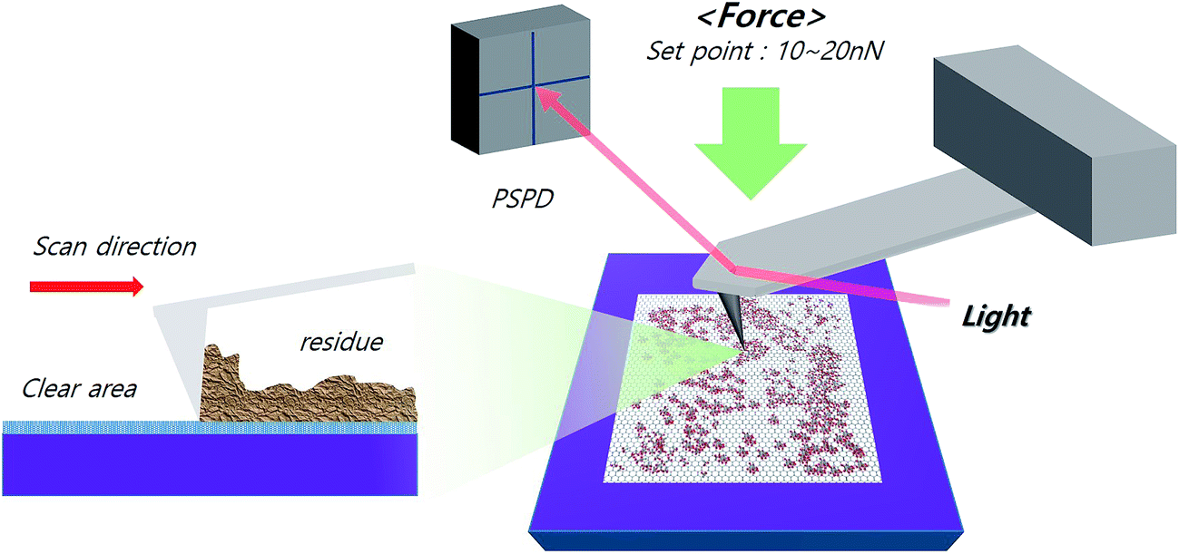 | ||
| Fig. 1 Schematic diagram of the AFM cleaning method. | ||
The CVD grown graphene was not damaged for the intermediate normal force from the tip, as it was durable. However, it was damaged via scanning at excessively high force (see ESI, Fig. S2†). Also, it was occasionally damaged at the beginning of the scanning, probably due to its high static frictional force. Thus, the sample was scanned with a small force at the beginning, and the force was gradually increased. This helped to prevent damage of the graphene, which was further confirmed by Raman measurement.
In order to confirm the removal of PMMA residue, the AFM topography was analyzed. Fig. 2(a) shows an optical microscopic image of CVD graphene transferred to Si/SiO2, which was scratched by a sharp blade as a mark. A red square in Fig. 2(a), depicts the area (10 × 10 μm2) for AFM cleaning. Fig. 2(b) and (d) show AFM topography images before and after cleaning, respectively. This confirms that the PMMA residue was brushed off, partially. However, some lumps of residue were found even after cleaning, in Fig. 2(d). As a result, the removal of residue by the AFM cleaning was not perfect, but it offers an adequate method to clean efficiently.
 | ||
| Fig. 2 (a) Optical image of CVD grown graphene transferred to SiO2. Red square indicates the cleaned area. AFM topographic image of transferred graphene before (b) and after (d) cleaning. (c) Line profiles before (along black line in (b)) and after (red line in (d)) the cleaning are shown. | ||
From comparison between line profiles extracted from the same location shown in Fig. 2(c), the base line after the cleaning was decreased about 3 nm, and peaks higher than 20 nm mostly disappeared. This shows that most large lumps of residue were removed. In comparison with Fig. 2(b) (before), some residues of PMMA in lower part of the scanned area became higher in the Fig. 2(d) as residue was gathered at the ends of the scanned area.
Surface roughness from AFM data can be used as a numerical evidence to quantify the removal effect. In this experiment, the root mean surface roughness values in Fig. 2 are 9.00 nm before cleaning and 8.51 nm after cleaning, respectively. The reduction of surface roughness was 0.49 nm, which is similar to others.22 But one can see that our roughness value is larger than that from the exfoliated graphene.22 This can be explained by the fact that, in the case of CVD graphene, bubbles and contaminants, as well as PMMA residue are trapped during the transfer process.
We confirmed that some residues scanned by AFM tip were shifted to the both sides and became lumpy, as shown in Fig. 3. After the second scan, one can see that lumpy residues were shifted to the right and grown gradually (Fig. 3(b)). Repeated scanning under the same conditions was performed as shown in Fig. 3(c), but this change was insignificant. As a result, once it was cleaned by scanning, the repeated scanning was not as effective as the first scanning. Those results also can be cross-checked by the lateral force microscopy (LFM) images, as shown in Fig. 3(d) and (f), simultaneously measured with the topographic images, respectively.
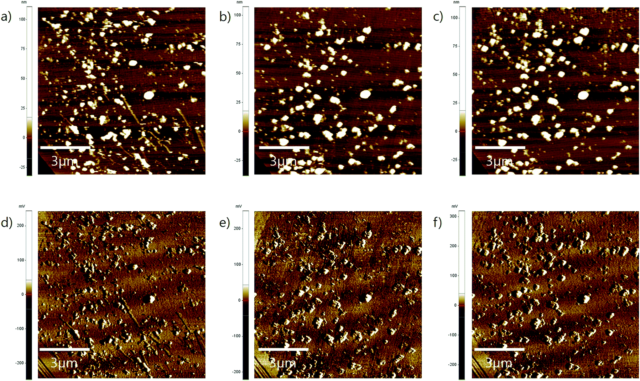 | ||
| Fig. 3 AFM images were taken at (a) 1st scan, (b) 2nd scan, and (c) 3rd scan in cleaning process. LFM images were obtained at (d) 1st scan, (e) 2nd scan, and (f) 3rd scan, also. | ||
For comparison, we conducted similar experiments on a mechanically exfoliated graphene sample. As shown in the ESI Fig. S3,† exfoliated graphene was cleaned, as explained before, to get a nearly perfectly cleaned surface. As CVD grown graphene has more defects which increase the probability of residues of PMMA, it was more difficult to clean than exfoliated graphene. Furthermore, the existence of winkles, grain boundaries, and trapped molecules under the graphene may cause the CVD grown graphene to be more strongly contaminated.
2. Raman spectroscopy
In order to investigate the effect of AFM cleaning on the electronic and crystalline property of graphene, the CVD grown graphene was analyzed using Raman spectroscopy. For comparison between the cleaned and uncleaned areas, the Raman mapping system was used for a wide scan area (20 × 18 μm2). Fig. 4(a)–(c) are the Raman mapping images of intensities of G, 2D, and D peaks from Raman spectra. The squares of white dotted line indicate the areas where the cleaning was done. Intensities of G and 2D peaks from cleaned area were slightly higher than the other area. These results indicated that the purity of graphene on the cleaned area was enhanced as the residues were removed. | ||
| Fig. 4 (a)–(c) Raman mapping images of graphene surface for G, 2D, and D peaks, respectively. (d) Raman spectroscopic data of graphene were taken from the cleaned (red line) and uncleaned (black line) area. The inset shows the microscopic image of the sample. (e) G and 2D peak intensities versus Raman shifts were plotted in an x–y graph, where uncleaned (black) and cleaned (red) locations are randomly selected. (f) D peak intensity versus Raman shift was plotted including uncleaned (black) and cleaned (red) locations. | ||
Raman data were quantitatively analyzed, comparing with the spectra at different locations of graphene in detail. In the Fig. 4(d), a representative spectrum with red line was taken from cleaned area, and a spectrum of black line was from uncleaned area. The peak intensities were increased by about 15%, for G and 2D bands, respectively. Comparing the images before and after the AFM cleaning, it was confirmed that the average intensity was increased about 5–7% after the AFM cleaning (see ESI, Fig. S4†). The G and 2D bands are representative signals originating from vibration of carbon atoms constituting graphene lattice. The residue of PMMA could weaken the Raman signal by partially blocking the laser beam.9 However, main reason of intensity increment should be related with removal of impurity, as the interactions between the carbon atoms and impurities were eliminated. The intensities of the D peak seem slightly different between the cleaned and uncleaned areas in Fig. 4(c), but a significant change of D peak was not found in the Fig. 4(f). The intensity of D peak related with defect of graphene33,34 was low, and the change of D peak was not clear. At least, the intensity of D peak was not increased, implying that there was no damage by AFM cleaning. This result shows that the damage by mechanical AFM cleaning was negligible, which was not found in prior papers reporting the AFM cleaning.20–22
After cleaning, the position of G peak and 2D peak was analyzed to investigate p-doping effect by the residue. In the Raman spectrum of un-doped graphene, G peak and 2D peak appear at about 1580 and 2680 cm−1. However, in the Fig. 4(e), G peak and 2D peak of uncleaned area were shifted to the left about 1–5 cm−1. Prior papers indicated that PMMA can be a source of p-type doping,35–37 and the position of the peaks were shifted to the left by p-doping.10 As a result of the data, CVD graphene transferred to Si/SiO2 was p-doped by the residue of PMMA. After the AFM cleaning, the positions of G peak and 2D peak were moved at 1581 cm−1 and 2678 cm−1, respectively closer to the positions of the un-doped graphene. Hence, the effect of p-doping was weakened by cleaning the residue of PMMA by using AFM tip. This result agrees with the Raman data of papers previously reported.10
3. Transconductance
We fabricated the CVD graphene based FETs, and the AFM cleaning was performed on the graphene surface. The electrical properties were investigated by measuring the residual doping and field effect mobility. Fig. 5(a) is an optical image of sample, where the graphene was patterned by using photolithography. The patterned graphene was connected to Au contact electrodes, and red circle indicates a cleaned area by AFM. An AFM topography image after the AFM cleaning is shown in Fig. 5(b). The central square is corresponding to the cleaned area and the outside is the uncleaned area. The cleaned area appears to be considerably smooth in comparison with the uncleaned area. Resistance of the conducting channel supported on the SiO2, including the cleaned area, was measured as a function of gate voltage applied to the Si substrate at room temperature in vacuum. The transconductance data were measured before (black line) and after (red line) the AFM cleaning, and representative data are shown in Fig. 5(c). Before cleaning, the Dirac peaks of samples were located at positive Vg = +21–33 V, while the Dirac peak of ideal un-doped graphene is zero. This result indicates that the CVD grown graphene was doped in p-type. After cleaning, Dirac peaks were found to be shifted toward the lower voltages (Vg = +7–22 V) (for list of Dirac peak shifts, see Table 1). This result agrees with other AFM cleaning papers20–22 and is explained by the removal of p-dopant. Prior papers reported that residue of PMMA was considered as a source of p-doping.35–38 The p-type dopants acted as electron acceptors, and H2O and O2 were adsorbed on residue surface. The decrease of p-doping can be explained by removal of residue due to AFM scanning. These results are compatible with the aforementioned Raman data analysis.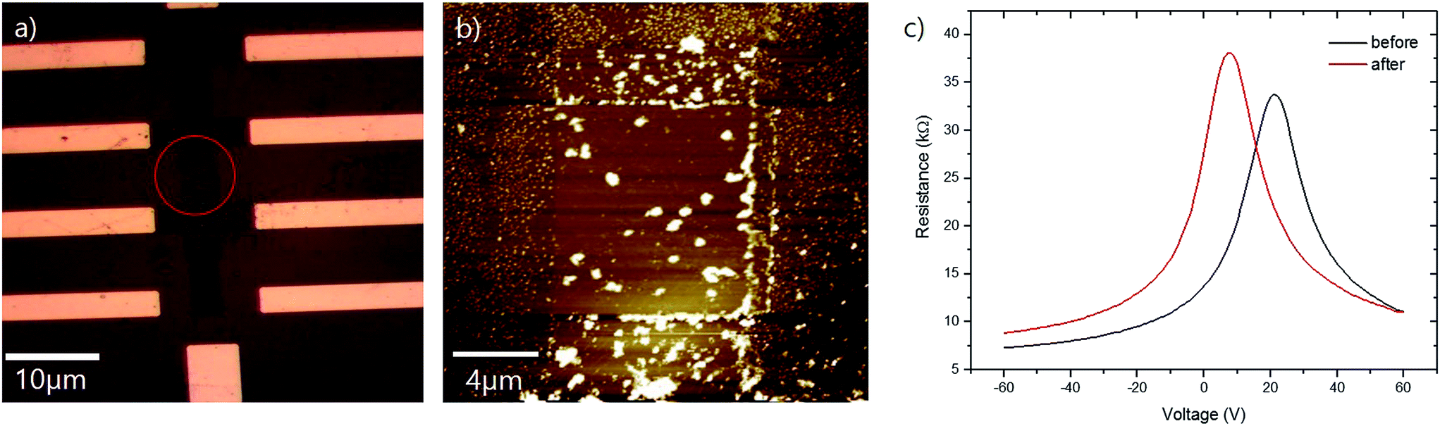 | ||
| Fig. 5 (a) Optical image of CVD grown graphene based FET, where red circle indicates the cleaned area. (b) AFM topographic image of the sample shows the cleaned state. (c) Resistances as functions of gate voltages were measured before (black line) and after (red line) the cleaning. | ||
| Sample name | Electron mobility (cm2 V−1 s−1) | Hole mobility (cm2 V−1 s−1) | Dirac point shift (V) | |||
|---|---|---|---|---|---|---|
| Before | After | Before | After | Before | After | |
| A | 788.2 | 842.5 | 631.5 | 702.0 | +33.0 | +22.1 |
| B | 789.9 | 835.3 | 645.8 | 617.9 | +21.6 | +8.4 |
| C | 2047.1 | 2257.5 | 1440.9 | 1500.3 | +24.2 | +7.9 |
| D | 716.0 | 849.3 | 619.8 | 630.3 | +22.3 | +7.6 |
As shown in Table 1, the carrier mobilities for four graphene based FET devices were increased up to 200 cm2 V−1 s−1 after AFM cleaning. In nearly all samples, increments of the mobility were confirmed after the cleaning (approximately 10%). This result also can be explained by removal of contamination causing carrier scattering. H2O and O2 adsorbed on residue surface result in an increase in carrier scattering, reducing the field effect mobility of graphene. Due to removal of residue, a source of p-type doping, carrier mobility was recovered. The increased value (10%) is less than that based on exfoliated graphene (80%) reported in other papers. In the case of CVD graphene, the graphene was synthesized to produce detects and grain boundaries, and the AFM cleaning does not remove the main causes of deterioration of mobility, such as detects and grain boundaries.39 In the case of exfoliated graphene, mobility is higher than that of CVD graphene, and the AFM cleaning can be more effective as the residue is reduced. In the paper of Lindvall et al., mobility of exfoliated graphene was increased by about 20% after the AFM cleaning.22 The mobility of the graphene can be further enhanced by reducing charged particles using electrostatic force.24
Conclusion
Here, we suggest an effective method to remove PMMA residues by using a contact-mode AFM on the surface of the CVD grown graphene. The proper loading force was in the range of 5 to 30 nN, for cleaning the graphene without damage. As a result of the AFM images, the removal of PMMA residue from the CVD graphene was clearly identified. To analyze the cleaning effects and damage due to the AFM cleaning, Raman spectroscopy was employed. From blue-shift of Raman spectrum after cleaning, we confirmed that p-doing effect by residue of PMMA was reduced. Also, G peak and 2D peak in Raman spectrum were intensified by the removal of the residue. Electrical properties of the CVD graphene based FETs on SiO2 were investigated. As the result, improvement of carrier mobility and shift of Dirac point were found. The AFM cleaning technique can be used to understand the basic characteristics of flow of electrons. Finally, we claim that our AFM cleaning technique can be a potential tool to clean the surface defects of 2D materials like TMDs, as well as graphene.Conflict of interest
The authors declare no competing financial interests.Acknowledgements
This research was supported by the Priority Research Centers Program (2010-0020207) through the National Research Foundation of Korea (NRF) funded by the Ministry of Education, and the Human Resources Development of the Korea Institute of Energy Technology Evaluation and Planning (KETEP) grant funded by the Korean government's Ministry of Trade, Industry & Energy (No. 20164030201340). Also, this work was supported by the industrial research innovation program (10051701), funded by the Ministry of Trade, Industry and Energy (MOTIE).References
- K. S. Novoselov, A. K. Geim, S. V. Morozov, D. Jiang, Y. Zhang, S. V. Dubonos, I. V. Grigorieva and A. A. Firsov, Science, 2004, 306, 666–669 CrossRef CAS PubMed.
- S. M. Kim, A. Hsu, P. T. Araujo, Y. H. Lee, T. Palacios, M. Dresselhaus, J. C. Idrobo, K. K. Kim and J. Kong, Nano Lett., 2013, 13, 933–941 CrossRef CAS PubMed.
- M. Buscema, D. J. Groenendijk, G. A. Steele, H. S. van der Zant and A. Castellanos-Gomez, Nat. Commun., 2014, 5, 4651 CrossRef CAS PubMed.
- A. Arab and Q. Li, Sci. Rep., 2015, 5, 13706 CrossRef PubMed.
- X. Chen, Y. Wu, Z. Wu, Y. Han, S. Xu, L. Wang, W. Ye, T. Han, Y. He, Y. Cai and N. Wang, Nat. Commun., 2015, 6, 7315 CrossRef CAS PubMed.
- L. Li, Y. Yu, G. J. Ye, Q. Ge, X. Ou, H. Wu, D. Feng, X. H. Chen and Y. Zhang, Nat. Nanotechnol., 2014, 9, 372–377 CrossRef CAS PubMed.
- N. R. Pradhan, D. Rhodes, S. Memaran, J. M. Poumirol, D. Smirnov, S. Talapatra, S. Feng, N. Perea-Lopez, A. L. Elias, M. Terrones, P. M. Ajayan and L. Balicas, Sci. Rep., 2015, 5, 8979 CrossRef CAS PubMed.
- A. Reina, X. Jia, J. Ho, D. Nezich, H. Son, V. Bulovic, M. S. Dresselhaus and J. Kong, Nano Lett., 2009, 9, 30–35 CrossRef CAS PubMed.
- Y. C. Lin, C. H. Jin, J. C. Lee, S. F. Jen, K. Suenaga and P. W. Chiu, ACS Nano, 2011, 5, 2362–2368 CrossRef CAS PubMed.
- A. Pirkle, J. Chan, A. Venugopal, D. Hinojos, C. W. Magnuson, S. McDonnell, L. Colombo, E. M. Vogel, R. S. Ruoff and R. M. Wallace, Appl. Phys. Lett., 2011, 99, 122108 CrossRef.
- R. S. Sundaram, C. Gomez-Navarro, E. J. H. Lee, M. Burghard and K. Kern, Appl. Phys. Lett., 2009, 95, 223507 CrossRef.
- A. Kozbial, F. Zhou, Z. Li, H. Liu and L. Li, Acc. Chem. Res., 2016, 49, 2765–2773 CrossRef CAS PubMed.
- Y. Dan, Y. Lu, N. J. Kybert, Z. Luo and A. T. Johnson, Nano Lett., 2009, 9, 1472–1475 CrossRef CAS PubMed.
- Z. Cheng, Q. Zhou, C. Wang, Q. Li, C. Wang and Y. Fang, Nano Lett., 2011, 11, 767–771 CrossRef CAS PubMed.
- J. Kedzierski, P. L. Hsu, A. Reina, J. Kong, P. Healey, P. Wyatt and C. Keast, IEEE Electron Device Lett., 2009, 30, 745–747 CrossRef CAS.
- M. Ishigami, J. H. Chen, W. G. Cullen, M. S. Fuhrer and E. D. Williams, Nano Lett., 2007, 7, 1643–1648 CrossRef CAS PubMed.
- W. Choi, Y.-S. Seo, J.-Y. Park, K. B. Kim, J. Jung, N. Lee, Y. Seo and S. Hong, IEEE Trans. Nanotechnol., 2015, 14, 70–74 CrossRef.
- K. I. Bolotin, K. J. Sikes, Z. Jiang, M. Klima, G. Fudenberg, J. Hone, P. Kim and H. L. Stormer, Solid State Commun., 2008, 146, 351–355 CrossRef CAS.
- J. Moser, A. Barreiro and A. Bachtold, Appl. Phys. Lett., 2007, 91, 163513 CrossRef.
- R. Jalilian, L. A. Jauregui, G. Lopez, J. F. Tian, C. Roecker, M. M. Yazdanpanah, R. W. Cohn, I. Jovanovic and Y. P. Chen, Nanotechnology, 2011, 22, 295705 CrossRef PubMed.
- A. M. Goossens, V. E. Calado, A. Barreiro, K. Watanabe, T. Taniguchi and L. M. K. Vandersypen, Appl. Phys. Lett., 2012, 100, 073110 CrossRef.
- N. Lindvall, A. Kalabukhov and A. Yurgens, J. Appl. Phys., 2012, 111, 064904 CrossRef.
- G. Fessler, B. Eren, U. Gysin, T. Glatzel and E. Meyer, Appl. Phys. Lett., 2014, 104, 041910 CrossRef.
- W. J. Choi, Y. J. Chung, S. Park, C. S. Yang, Y. K. Lee, K. S. An, Y. S. Lee and J. O. Lee, Adv. Mater., 2014, 26, 637–644 CrossRef CAS PubMed.
- D. Ferrah, O. Renault, C. Petit-Etienne, H. Okuno, C. Berne, V. Bouchiat and G. Cunge, Surf. Interface Anal., 2016, 48, 451–455 CrossRef CAS.
- F. Y. Shih, S. Y. Chen, C. H. Liu, P. H. Ho, T. S. Wu, C. W. Chen, Y. F. Chen and W. H. Wang, AIP Adv., 2014, 4, 067129 CrossRef.
- D. H. Tien, J. Y. Park, K. B. Kim, N. Lee and Y. Seo, Sci. Rep., 2016, 6, 25050 CrossRef CAS PubMed.
- S. Gahng, C. H. Ra, Y. J. Cho, J. A. Kim, T. Kim and W. J. Yoo, Appl. Phys. Lett., 2014, 104, 223507 CrossRef.
- W. Choi, Y. S. Seo, J. Y. Park, K. B. Kim, J. Jung, N. Lee, Y. Seo and S. Hong, IEEE Trans. Nanotechnol., 2015, 14, 70–74 CrossRef.
- A. Avsar, T. Y. Yang, S. Bae, J. Balakrishnan, F. Volmer, M. Jaiswal, Z. Yi, S. R. Ali, G. Guntherodt, B. H. Hong, B. Beschoten and B. Ozyilmaz, Nano Lett., 2011, 11, 2363–2368 CrossRef CAS PubMed.
- Y. G. Lee, C. G. Kang, U. J. Jung, J. J. Kim, H. J. Hwang, H. J. Chung, S. Seo, R. Choi and B. H. Lee, Appl. Phys. Lett., 2011, 98, 183508 CrossRef.
- A. Ambrosi and M. Pumera, Nanoscale, 2014, 6, 472–476 RSC.
- L. G. Cancado, A. Jorio, E. H. M. Ferreira, F. Stavale, C. A. Achete, R. B. Capaz, M. V. O. Moutinho, A. Lombardo, T. S. Kulmala and A. C. Ferrari, Nano Lett., 2011, 11, 3190–3196 CrossRef CAS PubMed.
- M. M. Lucchese, F. Stavale, E. H. M. Ferreira, C. Vilani, M. V. O. Moutinho, R. B. Capaz, C. A. Achete and A. Jorio, Carbon, 2010, 48, 1592–1597 CrossRef CAS.
- J. H. Chen, M. Ishigami, C. Jang, D. R. Hines, M. S. Fuhrer and E. D. Williams, Adv. Mater., 2007, 19, 3623–3627 CrossRef CAS.
- D. B. Farmer, R. Golizadeh-Mojarad, V. Perebeinos, Y. M. Lin, G. S. Tulevski, J. C. Tsang and P. Avouris, Nano Lett., 2009, 9, 388–392 CrossRef CAS PubMed.
- M. Na and S. W. Rhee, Org. Electron., 2006, 7, 205–212 CrossRef CAS.
- S. Ryu, L. Liu, S. Berciaud, Y. J. Yu, H. Liu, P. Kim, G. W. Flynn and L. E. Brus, Nano Lett., 2010, 10, 4944–4951 CrossRef CAS PubMed.
- P. Y. Huang, C. S. Ruiz-Vargas, A. M. van der Zande, W. S. Whitney, M. P. Levendorf, J. W. Kevek, S. Garg, J. S. Alden, C. J. Hustedt, Y. Zhu, J. Park, P. L. McEuen and D. A. Muller, Nature, 2011, 469, 389–392 CrossRef CAS PubMed.
Footnote |
| † Electronic supplementary information (ESI) available. See DOI: 10.1039/c6ra27436f |
| This journal is © The Royal Society of Chemistry 2017 |