
 Open Access Article
 This Open Access Article is licensed under a
 Creative Commons Attribution 3.0 Unported Licence
Electric field assisted growth and field emission properties of thermally oxidized CuO nanowires†
Chunmei Tanga,
Xinyue Liaob,
Weijie Zhonga,
Hongya Yua and
Zhongwu Liu *a
*a
aSchool of Materials Science and Engineering, South China University of Technology, Guangzhou, 510640, China. E-mail: zwliu@scut.edu.cn; Fax: +86-20-22236906; Tel: +86-20-22236906
bZhixin High School, No. 152, Zhixin South Road, Guangzhou, 510080, China
First published on 19th January 2017
Abstract
An electric field was introduced into the thermal oxidation synthesis of CuO nanowires (NWs) by heating Cu foils at 400 °C under ambient conditions using a hotplate. The morphology and crystal structure of the NWs on both sides of the foils synthesized under different electric field intensities and directions were characterized. The results indicated that adding an electric field increases the length and density of the CuO NWs. Particularly, the electric field can promote the growth of the NWs with the growing direction parallel to the electric field through accelerating the diffusion of Cu ions. Interestingly, a downward electric field and an upward temperature gradient change the growth direction of NWs on the bottom surface of the Cu foils. Besides, adding a downward electric field can increase the yield of CuO NWs with large aspect ratio, as they can grow on both sides of the Cu foil. The field emission properties of CuO NWs obtained under different electric fields indicated that these nanowire arrays could be used as the cathode of field emission displays.
1. Introduction
Nanoscale transition metal oxide nanostructures have been attracting much attention in recent years because of their unique physical and chemical properties as well as promising applications in micro/nanoscale devices.1–4 Cupric oxide (CuO) is a p-type semiconductor with a narrow band gap, and it has shown attractive properties and potential applications in field emissions,5 gas/bio sensors,6 photo detectors,7 photocatalysis,8 and superconductors.9 Thermal oxidation is a very simple, efficient, low temperature, and low-cost preparation method, which is suitable for the large scale synthesis of nanostructures.10–12 Many research groups13–15 have confirmed the feasibility of this simple method for growing CuO nanowires (NWs), but more effort is needed to study the growth mechanisms and more methods to control the growth morphology are needed.Theoretically, in thermal oxidation process, CuO NW growth is primarily governed by the diffusion and the reaction of Cu ions and O ions.14 Therefore, it is possible to control the growth and morphology of CuO nanostructures by adding an external electric or magnetic field to modify the velocity and direction of ion diffusion. Li et al.16 employed an electric field (0–5000 V m−1) on the Cu films during heating in the furnace at 600–730 °C, and they found that the length of the CuO nanoneedles increased with the electric field and the diameter became smaller and more uniform when the voltage was smaller than a certain value. Furthermore, Farbod et al.17 investigated the effect of high electric fields (13![[thin space (1/6-em)]](https://www.rsc.org/images/entities/char_2009.gif) 000–130000 V m−1) on the growth of CuO NWs at a relatively low temperature (500 °C) and found that annealing in the electric field increased the wire density, adhesion, and uniformity in diameter of the NWs. However, these previous works mainly focused on the effect of the electric intensity on the growth of Cu nanostructures on the top side only. It remains a question how the direction and intensity of the field affect the growth, morphology, and field emissions of the CuO NWs, especially under the consideration of the temperature configuration.
000–130000 V m−1) on the growth of CuO NWs at a relatively low temperature (500 °C) and found that annealing in the electric field increased the wire density, adhesion, and uniformity in diameter of the NWs. However, these previous works mainly focused on the effect of the electric intensity on the growth of Cu nanostructures on the top side only. It remains a question how the direction and intensity of the field affect the growth, morphology, and field emissions of the CuO NWs, especially under the consideration of the temperature configuration.
In order to enhance the field emission properties, the researchers employed various approaches to obtain surface modified,18,19 hybrid,20,21 and post-processed22,23 CuO nanostructures. Recently, noble metal nanoparticles, such as Ag18 and Au,24 are decorated on the 1D CuO nanostructures by wet chemistry and enhanced field emissions have been obtained due to the increased conductivity and improved semiconductor characteristics. Carbon materials (graphene oxide layers19 and carbon nanotube network films25) and metal oxides such as ZnO nanoparticles26 are also chosen to coat on the CuO nanostructures to improve the field emissions. Good field emitters have been made of 3D CuO nanowires produced by heating Cu rods fabricated by through silicon via process.5 However, there are no reports about the field emission properties of oxide nanostructures prepared under an electric field.
We recently found that the adhesion and field emission properties of CuO NWs can be enhanced by a simply modified thermal oxidation method using hotplate,27 which supplies a stable oxidation environment by introducing two stainless steel plates on the top and bottom of the Cu substrate. In this work, an electric field was further introduced on the two plates at a relatively low fixed temperature of 400 °C. The effects of field intensity and direction on the morphology, structure, and field emissions of CuO NWs were illustrated. The current research is important to realize the controllable synthesis of CuO nanomaterials and promote their practical applications in functional devices.
2. Experimental
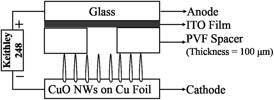
CuO nanostructures were grown on Cu foils by an electric field assisted thermal oxidation method. Before heating, the 99.999% pure Cu foils (0.2 mm) were polished, cleaned, and prepared, as described elsewhere.27 Fig. 1 shows that the Cu foil is placed between two steel plates with 3 mm on the hotplate. Various DC voltages (0 V, 30 V, and 50 V) were exerted between two plates and the field direction was set upwards and downwards. Cu foils were heated in ambient air at 400 °C for 0.5 h to 48 h. Black films were formed on both sides of the foil after heating, and their typical SEM images were also shown in Fig. 1. It is noted that an upward temperature gradient generally exists during hotplate heating. The temperature in the vertical direction decreases upwards from the top surface of hotplate to the air.27 | ||
| Fig. 1 Schematic diagram for illustrating the fabrication process of the electric field assisted thermal oxidation with different directions and typical morphologies after heating. | ||
The morphologies and crystalline structures of CuO NWs synthesized under different electric field directions (upward and downward), electric field intensities (0, 100, and 166.67 V cm−1), and with various heating durations were characterized via a field emission scanning electron microscopy (FEI Nova Nano SEM 430) and X-ray diffraction (Philips X'Pert, Cu Kα, λ = 0.15406 nm). The schematic configuration for field emission test system (Shenyang Tiancheng vacuum Technology Co., Ltd.) are shown in Fig. 2. The CuO NWs cathode and ITO anode are separated by polyvinyl fluoride (PVF) spacer with a thickness of 100 μm.
 | ||
| Fig. 2 Schematic diagram of the configuration for field emission measurements. | ||
3. Results and discussion
Non-flaking black films were obtained on the top surface of all Cu foils after heating, which were fully exposed to the ambient air. Black films were also formed on the bottom of the foil, which directly contacted the steel plate with relatively low air concentration. As described previously,27 this simply modified thermal oxidation setup is effective to enhance the adhesion between the oxides and Cu substrate, regardless of the intensity and direction of the applied electric field.3.1 Influences of an upward electric field
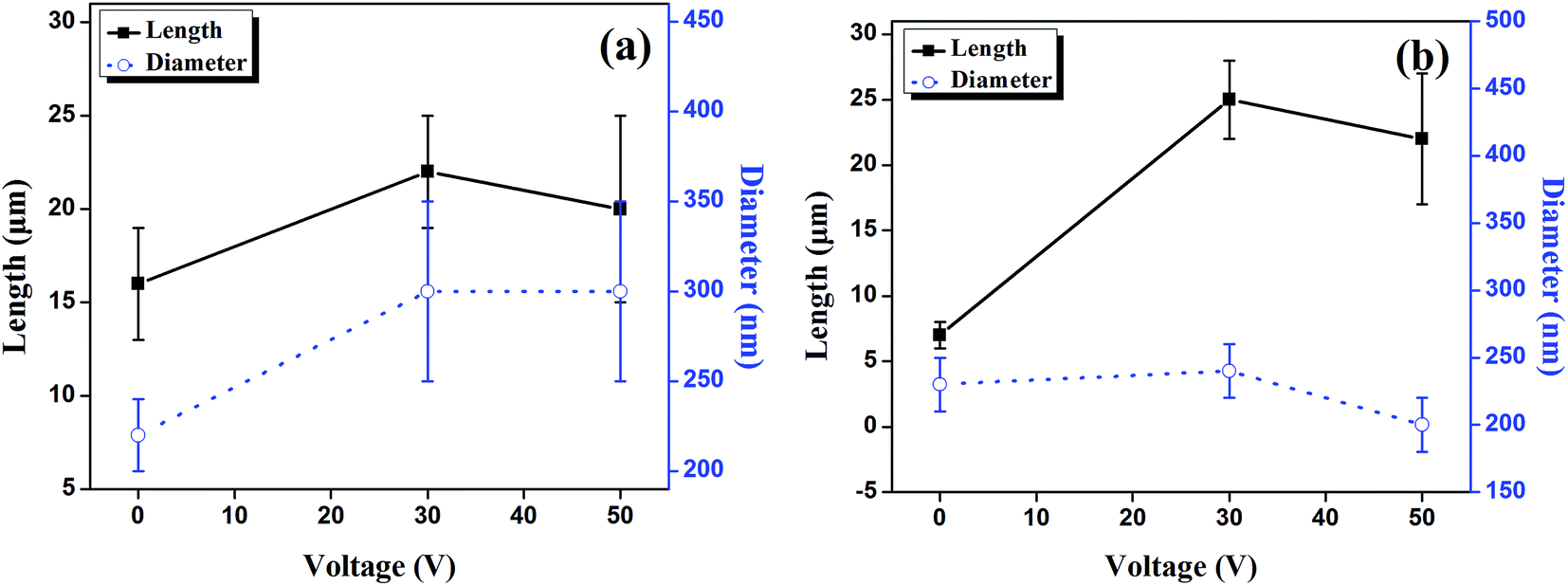
The samples prepared under different upward electric field intensities are shown in Fig. 3. The applied voltages of 0, 30, and 50 V are corresponding to the electric field intensities of 0, 100.00, and 166.67 V cm−1, respectively. Fig. 4 give the relationships between the NW length/diameter and the voltage. Based on our previous investigations,27 CuO NWs with good adhesion to Cu substrate are successfully obtained between the two plates on the hotplate with 0 V voltage. Under different field intensities, the NWs show different dimensions. Fig. 3a–c show that tapered CuO NWs are grown on all the top surfaces with direction perpendicular to the substrate. Adding a voltage of 30 or 50 V increases the length of CuO NWs from about 15 μm to 20 μm or 30 μm, respectively. Fig. 3d–f show that all the bottom surfaces were covered with some short, thick bar-like nanostructures. As far as the dimension is concerned, the NWs on bottom surface are not as good as those on top surface under the same condition. Most of the nanorods in Fig. 3e were broken off and left roots about 1 μm alone while being prepared for SEM, indicating that the nanorods on the bottom surface are unstable. The results indicate that introducing and increasing the intensity of an upward electric field promotes the growth of CuO NWs on the top surface, which are similar to the reported works.16,17 Meanwhile, the NWs on the bottom surface become thicker.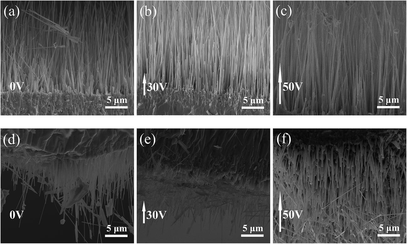 | ||
| Fig. 3 Cross-sectional SEM images of the top and bottom surfaces of Cu foils under various upward electric fields (↑): top surface (a) 0 V, (b) 30 V, (c) 50 V; bottom surface (d) 0 V, (e) 30 V, (f) 50 V. | ||
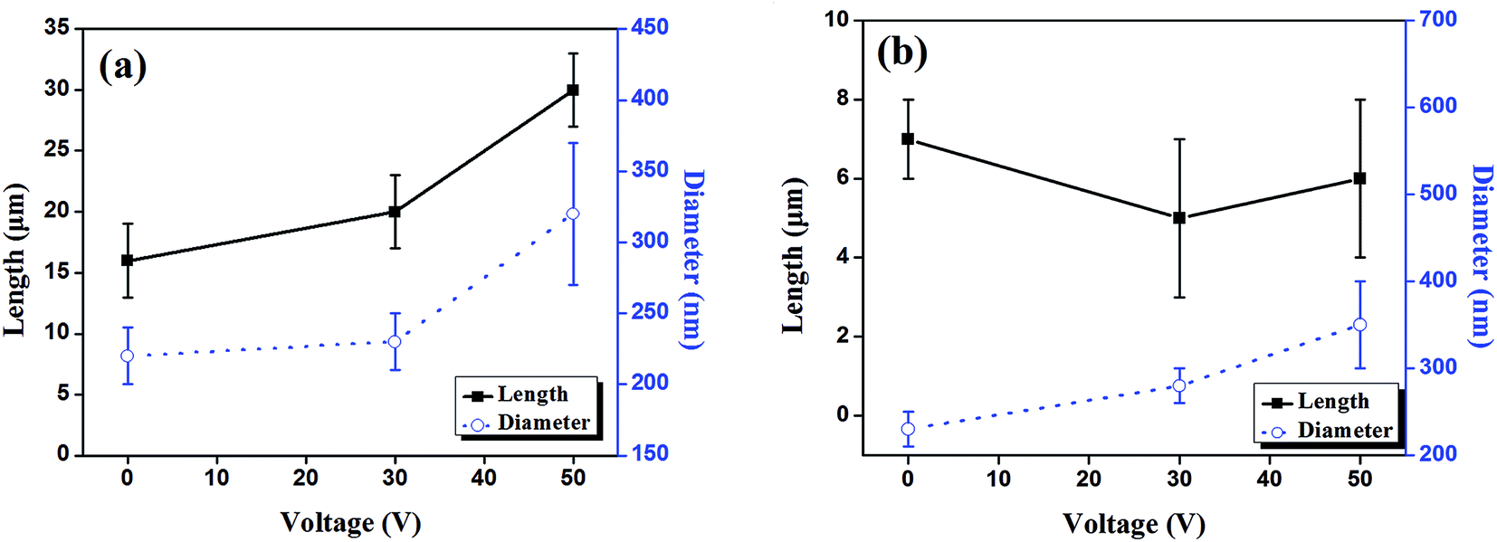 | ||
| Fig. 4 Voltage vs. length and voltage vs. diameter curves of CuO NWs on (a) top surfaces and (b) bottom surfaces of Cu foils under different upward electric field intensities (↑). | ||
3.2 Influences of a downward electric field
The samples prepared under different downward electric field intensities (30 and 50 V) are shown in Fig. 5. The plots of voltage vs. length and voltage vs. diameter curves are shown in Fig. 6. Fig. 5a and b show that the NWs on the top surfaces, which are prepared with an electric field opposite to the temperature gradient, are little longer and thicker than that prepared without field (Fig. 3a). Fig. 5c and d show that a downward electric field clearly promotes the growth of CuO NWs on the bottom surface, leading to the increased length from several micrometers (Fig. 3d) to >20 micrometers. However, the field intensity in the range of 30–50 V has little effect on the nanowire growth on both sides. Interestingly, the growth directions of the NWs in Fig. 5c and d are found to be significantly different from others. They did not grow perpendicular to the substrate but with some angle to the vertical plane and finally became parallel to the surface. This behavior should be the result of the interacting effect of an upward temperature gradient and a downward electric field.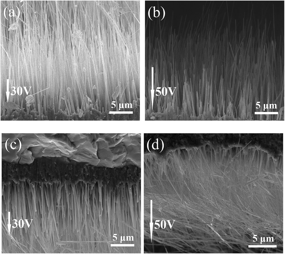 | ||
| Fig. 5 Cross-sectional SEM images of the top and bottom surfaces of Cu foils under different downward electric fields (↓): top surface (a) 30 V, (b) 50 V; bottom surface (c) 30 V, (d) 50 V. | ||
 | ||
| Fig. 6 Voltage vs. length and voltage vs. diameter curves of CuO NWs on (a) top surfaces and (b) bottom surfaces of Cu foils under different downward electric field intensities (↓). | ||
Above results clearly indicated that the electric field can promote the growth of NWs with growth direction parallel to the electric field direction, but has less effect on the NWs on the other surface if the direction of temperature gradient remains the same. Furthermore, as oxidations are always existed on two sides during heating, applying a downward electric field can increase the yield and quality of CuO NWs with large aspect ratio. Therefore, the length, diameter, density, and direction of NWs can be successfully changed through adjusting the electric field.
3.3 Influences of the heating duration
The cross-sectional SEM images of Cu foils heated at 400 °C with an upward electric field of 166.67 V cm−1 (50 V) for various time from 0.5 h to 48 h are shown in Fig. 7a–e. Only a few sharp, thin, and straight CuO NWs with varied lengths are found on Cu substrate heated for 0.5 h (Fig. 7a). This result indicates that only a small amount of Cu ions which obtained sufficient energy can react with oxygen and grow preferentially when the heating time is too short. Many short CuO NWs nucleate and grow on a large scale after 2 h (Fig. 7b). It is clearly from Fig. 7c–e that the length of the NWs exhibits a substantial increase and the NW diameter increases to 200 nm when heating over 8 h. Fig. 7f is the dependences of the NWs length and diameter on the heating time. Both the length and diameter increase with the heating time, although they may follow different laws. Therefore, the growth of CuO NWs synthesized by electric field assisted thermal oxidation involves four steps. At first, a few NWs nucleate and grow preferentially. Second, CuO NWs nucleate on a large scale. Third, the length and diameter increase. Finally, the NWs grow much longer.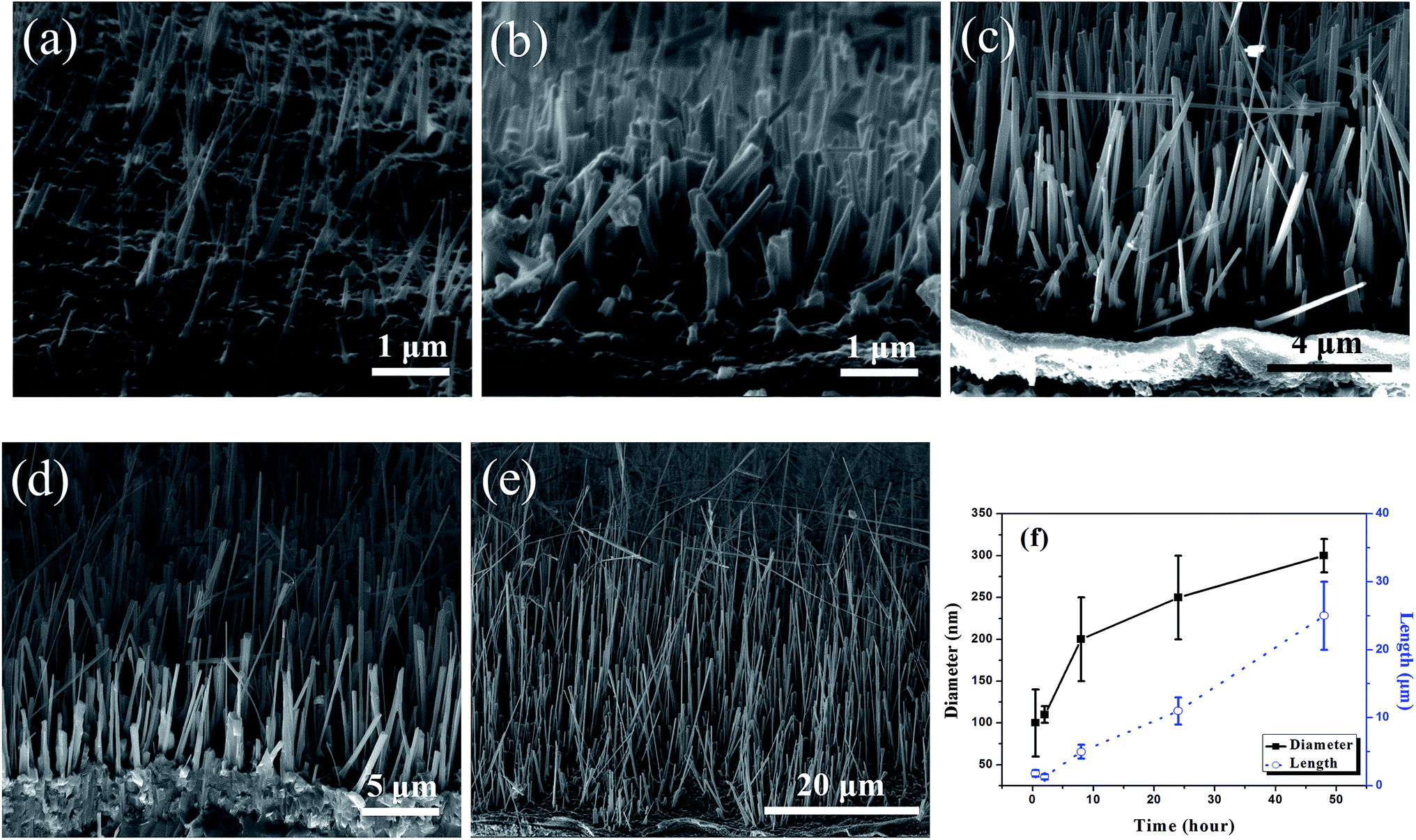 | ||
| Fig. 7 Cross-sectional SEM images of Cu foils heated at 400 °C with an upward electric field of 166.67 V cm−1 (50 V) for (a) 0.5 h, (b) 2 h, (c) 8 h, (d) 24 h, (e) 48 h, and (f) the corresponding time vs. length and time vs. diameter curves. | ||
3.4 Phase structure and layer structure of thermally oxidized products
The XRD patterns of the samples synthesized in different electric fields are shown in Fig. 8. CuO and Cu2O phases are detected in all samples. The appearance of Cu2O means that NWs do not grow directly from the Cu substrate, a behavior which coincides with most previous researches.12,15,28 The intensities of CuO peaks on the top surface were stronger than bottom surface for the samples prepared in 0 V and upward 50 V, indicating that the NWs preferably grow on the top surface. But for the samples prepared under a downward electric field, the CuO and Cu2O peaks have strong intensity on both sides, indicating that the nanowire grows well on both sides. In addition, the peak intensities of CuO phase on bottom surface are stronger than that on bottom surface, which results from the fact that a downward electric field can significantly promote the NWs growth on the bottom surface. The phase structure results are in good agreement with those in SEM images (Fig. 3 and 5).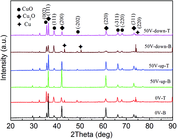 | ||
| Fig. 8 XRD patterns of Cu foils heated in different electric fields, where “up” and “down” mean the direction of electric field, T represents the top surface, and B represents the bottom surface. | ||
The oxide layers of Cu foils after heating under electric fields (Fig. 9) are similar to those obtained between two plates without an applied field (0 V).27 As shown in Fig. 9, the oxidized samples prepared under different electric field directions have a three-layer structure of CuO NWs/CuO layer/Cu2O layer, and the Cu2O layer is much thicker than the CuO layer. The results indicate that the nucleation and growth of CuO NWs are based on the oxide layers rather than Cu substrate, which was confirmed by many researches.12,14,27
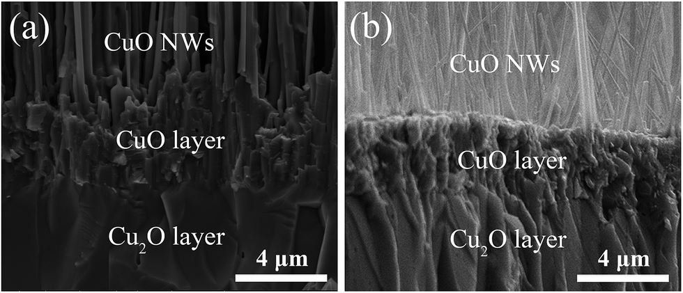 | ||
| Fig. 9 Cross-sectional SEM images of layers' structure of Cu foils after heated in (a) 50 V-upward and (b) 50 V-downward electric field. | ||
3.5 Underlying mechanism of electric field assisted-thermal oxidation
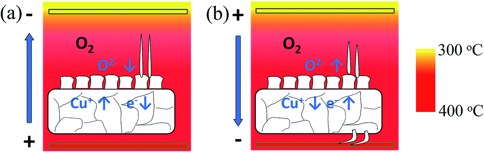
The effect of electric field direction on the ion diffusion can be employed to explain the differences in the CuO NW morphology. The growth of CuO NWs is a result of the reaction between Cu ions and O ions by 4Cu + O2 → 2Cu2O, and 2Cu + O2 → 2CuO.12 Hence, the ions supply is a key factor governing its growth. Although CuO NWs are found on both sides of the Cu substrate, their growth condition is different. The Cu ions supplies on two sides are similar, but the oxygen conditions are different. The Cu ions on the top surface are easy to get enough oxygen because they are directly contact with air. But the Cu ions on the bottom surface, which are directly contact the bottom plate, are relatively lacking of oxygen. Furthermore, the growing direction of CuO NWs on the top surface is along the upward temperature gradient in the hotplate, which is very important for thermal oxidation growth.27 Therefore, the Cu ions on the top surface are much easier to grow into NWs than those on the bottom surface under same temperature and voltage condition (Fig. 3a and d).El Mel et al.29 proposed that the diffusion of metal ions occurs due to the thermally activated ion diffusion and field driven diffusion. Field driven diffusion process is dominant at low temperatures, while the thermally activated ion diffusion becomes dominant as the temperature increases. The temperature employed in this work is only 400 °C, so the diffusion of metal ions is affected by both processes. Fig. 10a shows that an upward electric field makes Cu ions move upward, while O ions and electrons move downward. The Cu ions and O ions meet and react on the surface to form CuO NWs. The temperature gradient and electric field makes the Cu ions on the top surface move upward along the growing direction of the NWs, so they are the longest and the densest (Fig. 3b and c). On the contrary, the NWs on bottom surface are easy to grow short and stubby due to the opposite growing direction and lack of oxygen (Fig. 3e and f). Although the electric field makes O ions and electrons move downward, it is difficult for the O ions on the top surface to pass the copper layer and combine with the Cu ions on the bottom surface. Moreover, its movement is also hampered by the upward temperature gradient. Lack of oxygen also makes it difficult for the generation of O ions on the bottom surface.
 | ||
| Fig. 10 Schematics for the effect of the (a) upward and (b) downward electric field directions on ion motion during the thermal oxidation of Cu foils. | ||
Fig. 10b shows that a downward electric field makes Cu ions move downward and O ions and electrons upward. As a result, the NWs on the top surface are relatively shorter and thicker than those obtained under same upward field intensities. The downward movement of Cu ions, which is along their growth direction on the bottom surface, promote NWs growth significantly (Fig. 5c and d). The top of NWs on the bottom surface are away from the substrate and close to the hotplate when they grow longer. So, the effect of the electric field becomes less significant while the thermally activated diffusion increases. The combination of the effects of the opposite electric field and temperature gradient lead to a deflection of the nanowire and finally the tips of the NWs are parallel to the substrate surface (Fig. 5c and d).
When no electric field is employed, the diffusion of ions is mainly controlled by the temperature. Most Cu ions in the substrate have not gotten enough energy to move and react with oxygen on the tips of NWs, so the NWs are shorter and thinner with smaller tip radius. Therefore, adding an electric field can promote the movement of ions to pass through the oxide layer and diffuse along the NW, which leads to longer and denser NWs.
3.6 Field emission properties
The special morphology of the NWs has importance for field emission applications. Here we tested the field emission properties of the samples prepared without electric field (0 V), with 50 V upward, and 50 V downward voltages. To characterize the field emission properties, the turn-on field is defined as the electric field intensity at a current density of 10 μA cm−2. The threshold field is defined as the intensity at 1 mA cm−2, Jmax is the measured maximum current density, and Emax is the field intensity at the maximum current density.According to the well-known Fowler–Nordheim equation, the current density J (A cm−2) can be expressed as:30
 | (1) |
 | (2) |
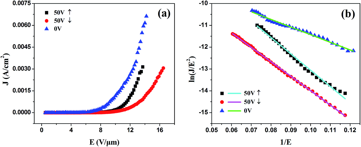
The J–E curves and F–N plots for our NWs are shown in Fig. 11a and b, respectively. The relevant properties and structure parameters, such as length, diameter, and density, are also shown in Table 1. In our previous work,27 the field emission properties of CuO NWs obtained between two plates (0 V) are much better than that from direct thermal oxidation, which may result from the stable, straight, and long NWs with sharp tips, appropriate density, and crack elimination. In this work, the field emission properties of the three samples are all better than that from direct thermal oxidation. The current density of all the CuO NWs samples has reached 1 mA cm−2, which indicated that they can be used as the cathode of field emission display. The good linearity of F–N plots (Fig. 11b) at high field means the emission mechanism is quantum tunneling.
 | ||
| Fig. 11 (a) Field emission J–E curves and (b) corresponding Fowler–Nordheim (F–N) plots of CuO NWs prepared under different electric field. | ||
| 0 V | 50 V-up (↑) | 50 V-down (↓) | ||
|---|---|---|---|---|
| a Note: length–diameter ratio is obtained through dividing length by diameter(Root). | ||||
| Morphology parameters | Length (μm) | 16 ± 2 | 30 ± 3 | 16 ± 3 |
| Diameter(Tip) (nm) | 80 ± 10 | 100 ± 20 | 110 ± 30 | |
| Diameter(Root) (nm) | 220 ± 20 | 320 ± 50 | 250 ± 30 | |
| Length–diameter ratio | 74.2 ± 15.8 | 97.6 ± 24.6 | 66.4 ± 20 | |
| Density (per cm2) | (1.97 ± 0.28) × 108 | (2.26 ± 0.3) × 108 | (1.01 ± 0.2) × 108 | |
| Field emission parameters | Eturn-on (V μm−1) | 5.31 | 7.11 | 8.1 |
| E1 mA cm−2 (V μm−1) | 9.8 | 11.9 | 13.9 | |
| Jmax (mA cm−2) | 6.62 | 3.14 | 3.06 | |
| Emax (V μm−1) | 14.2 | 13.7 | 16.5 | |
| SFN | −35.0 | −74.8 | −65.3 | |
| β | 1863 | 871 | 998 | |
Fig. 11 and Table 1 show that although the NWs prepared under an upward 50 V voltage have largest length, aspect ratio and density, its field emission performance is not the best. In order to analyze the properties better, the SEM images of the tip of NWs are shown in Fig. S1.† Their thicker tip diameters (∼100 nm) without sharp tips are not beneficial for the field emission (Fig. S1b†). The SEM images of the upper part of 50 V upward also show significant bending and lodging, as the NWs are too long (Fig. S2†). Many impurities are also found on the tips of the intertwined NWs (Fig. 3c). In addition, the overcrowding NWs generally lead to screening effect.33 All of those greatly reduce their field emission properties. The field emission properties of the NWs prepared at a downward 50 V voltage is worst, with the highest turn-on field (8.1 V μm−1) and threshold field (13.9 V μm−1), and lowest Jmax (3.06 mA cm−2). The smallest aspect ratio and density as well as the large tip diameter should be responsible for their relatively bad properties. Compared to these two samples, the NWs prepared at 0 V have proper density and smallest diameter with sharp tips (∼80 nm), which are beneficial for the field emission.34
As we know, the field enhancement factor is defined as the ratio of the local field to the applied field, which is most related to the aspect ratio, but the density and shape also have great effect. Although most of the work related to the field emission studied the field enhancement factor β, many definitions of β are proposed to explain the results.35 Some reports suggest that β is proportionally related to value of height of the emitters over the radius of curvature of tip. Ye et al.36 proposed that the field enhancement factor is determined by the shape and morphology of the emitters, proportional to the screening factor (s), and inverse proportionally related to the tip radius of the emitters (r), as shown in formula: 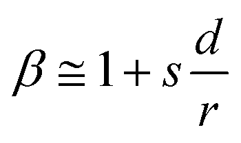 . The screening factor s become smaller when the emitter are densely packed. In spite of the highest aspect ratio of CuO NWs obtained at the 50 V-up, the relatively thicker tip radius and high density are not good for the β, making it smaller than 0 V (Table 1). So the NWs prepared at 0 V show the best field emission properties, with minimum turn-on field (5.31 V μm−1), lowest threshold field (9.8 V μm−1), maximum Jmax (6.62 mA cm−2), and largest enhancement factor β (1863). The field emissions properties obtained in this work are comparable to thermally oxidized CuO NWs after UV-illumination22 and low-energy Ar ion bombardment,23 whose best turn-on field is 5.16 V μm−1 and 5.25 V μm−1, respectively.
Above results indicate that the stable emission and reception of electrons are the keys of good field emission properties, which are associated with the specific morphology, growth direction and vertical stability of the NWs and so on. In the present work, although the electric field has a significant impact on growth and morphology of CuO NWs, it does not further improve the field emission properties yet. However, it can be believed that the field emission can be enhanced by designing oxidation process to make full use of the beneficial effects of both electric field and temperature gradient. By that way, the CuO NWs with sharp tips, proper density, and high aspect ratio but proper length can be achieved.
4. Conclusions
CuO NWs were successfully obtained on both sides of the Cu foils by a simple electric field assisted thermal oxidation method. Adding an electric field can increase length and density of thee NWs with growing direction parallel to the field through promoting the movement of ions to pass through the oxide layer and diffuse along the NW. Hence, an upward electric field can be used for the growth of extraordinarily long NWs, and a downward field increases the yield of CuO NWs with large aspect ratio on both sides. It provide more approaches to obtain the designed morphology by adjusting the temperature gradient and electric field. The relatively low temperature and voltage of this method broaden its applications for Cu oxidation on different substrates, especially for those metal substrates which cannot resist high temperature heating. Although the field emission properties have not been greatly improved, the synthesized CuO NWs with large aspect ratio reveal potential in other applications, such as gas sensors and photocatalysis.Acknowledgements
This work is partly supported by the Fundamental Research Funds for the Central Universities (Grant no. 2015ZP030). The field emission measurements by Prof. Xiaohong Ji at South China University of Technology are gratefully acknowledged.References
- R. S. Devan, R. A. Patil, J.-H. Lin and Y.-R. Ma, Adv. Funct. Mater., 2012, 22, 3326–3370 CrossRef CAS.
- Q. Zhang, K. Zhang, D. Xu, G. Yang, H. Huang, F. Nie, C. Liu and S. Yang, Prog. Mater. Sci., 2014, 60, 208–337 CrossRef CAS.
- J. Wang, Q. Zhang, X. Li, B. Zhang, L. Mai and K. Zhang, Nano Energy, 2015, 12, 437–446 CrossRef CAS.
- J. Zhang, X. Liu, G. Neri and N. Pinna, Adv. Mater., 2016, 28, 795–831 CrossRef CAS PubMed.
- Y. M. Juan, S. J. Chang, H. T. Hsueh, S. H. Wang, T. C. Cheng, S. W. Huang, T. J. Hsueh, Y. M. Yeh and C. L. Hsu, RSC Adv., 2016, 6, 47292–47297 RSC.
- J.-S. Lee, A. Katoch, J.-H. Kim and S. S. Kim, Sens. Actuators, B, 2016, 222, 307–314 CrossRef CAS.
- T. Zhai, X. Fang, M. Liao, X. Xu, H. Zeng, B. Yoshio and D. Golberg, Sensors, 2009, 9, 6504–6529 CrossRef CAS PubMed.
- L. Zhao, T. Cui, Y. Li, B. Wang, J. Han, L. Han and Z. Liu, RSC Adv., 2015, 5, 64495–64502 RSC.
- X. J. Zhang, W. H. Shi, J. X. Zhu, D. J. Kharistal, W. Y. Zhao, B. S. Lalia, H. H. Hng and Q. Y. Yan, ACS Nano, 2011, 5, 2013–2019 CrossRef CAS PubMed.
- X. C. Jiang, T. Herricks and Y. N. Xia, Nano Lett., 2002, 2, 1333–1338 CrossRef CAS.
- J. T. Chen, F. Zhang, J. Wang, G. A. Zhang, B. B. Miao, X. Y. Fan, D. Yan and P. X. Yan, J. Alloys Compd., 2008, 454, 268–273 CrossRef CAS.
- M. L. Zhong, D. C. Zeng, Z. W. Liu, H. Y. Yu, X. C. Zhong and W. Q. Qiu, Acta Mater., 2010, 58, 5926–5932 CrossRef CAS.
- A. M. B. Gonçalves, L. C. Campos, A. S. Ferlauto and R. G. Lacerda, J. Appl. Phys., 2009, 106, 034303 CrossRef.
- L. Yuan, Y. Wang, R. Mema and G. Zhou, Acta Mater., 2011, 59, 2491–2500 CrossRef CAS.
- Q. Zhang, J. Wang, D. Xu, Z. Wang, X. Li and K. Zhang, J. Mater. Chem. A, 2014, 2, 3865 CAS.
- X. Li, J. Zhang, Y. Yuan, L. Liao and C. Pan, J. Appl. Phys., 2010, 108, 024308 CrossRef.
- M. Farbod, N. Meamar Ghaffari and I. Kazeminezhad, Ceram. Int., 2014, 40, 517–521 CrossRef CAS.
- S. Wu, F. Li, L. Zhang and Z. Li, Mater. Lett., 2016, 171, 220–223 CrossRef CAS.
- W. Yu, H. Hu, D. Zhang, H. Huang and T. Guo, J. Vac. Sci. Technol., B: Nanotechnol. Microelectron.: Mater., Process., Meas., Phenom., 2016, 34, 02G102 Search PubMed.
- Y.-M. Juan, S.-J. Chang, H.-T. Hsueh, S.-H. Wang, T.-C. Cheng, S.-W. Huang and C.-L. Hsu, RSC Adv., 2015, 5, 54220–54224 RSC.
- C.-L. Hsu, J.-Y. Tsai and T.-J. Hsueh, RSC Adv., 2015, 5, 33762–33766 RSC.
- J. Zhao, D. Wang, Y. Chen, Q. Jin and G. Wang, Nano, 2016, 11, 1650056 CrossRef CAS.
- X. Song and J. Chen, Appl. Surf. Sci., 2015, 329, 94–103 CrossRef CAS.
- F. Li, S. Wu, L. Zhang and Z. Li, Appl. Phys. A, 2015, 120, 1383–1389 CrossRef CAS.
- H. Hu, D. Zhang, Y. Liu, W. Yu and T. Guo, Vacuum, 2015, 115, 70–74 CrossRef CAS.
- L. Sun, C. X. Wu, X. T. Zhou, Y. A. Zhang and T. L. Guo, Mater. Technol., 2014, 30, 177–181 CrossRef.
- C. M. Tang, Y. B. Wang, R. H. Yao, H. L. Ning, W. Q. Qiu and Z. W. Liu, Nanotechnology, 2016, 27, 395605 CrossRef CAS PubMed.
- L. Yuan and G. Zhou, J. Electrochem. Soc., 2012, 159, C205–C209 CrossRef CAS.
- A. A. El Mel, M. Buffiere, N. Bouts, E. Gautron, P. Y. Tessier, K. Henzler, P. Guttmann, S. Konstantinidis, C. Bittencourt and R. Snyders, Nanotechnology, 2013, 24, 265603 CrossRef CAS PubMed.
- L. W. Nordheim, Proc. R. Soc. A, 1928, 121, 626–639 CrossRef.
- Y. W. Zhu, T. Yu, F. C. Cheong, X. J. Xu, C. T. Lim, V. B. C. Tan, J. T. L. Thong and C. H. Sow, Nanotechnology, 2005, 16, 88–92 CrossRef CAS.
- T. Utsumi, IEEE Trans. Electron Devices, 1991, 38, 2276–2283 CrossRef.
- L.-C. Hsu, Y.-Y. Li and C.-Y. Hsiao, Nanoscale Res. Lett., 2008, 3, 330–337 CrossRef CAS.
- H.-F. Hsu, J.-Y. Wang and Y.-H. Wu, J. Electrochem. Soc., 2014, 161, H53–H56 CrossRef.
- C. M. Collins, R. J. Parmee, W. I. Milne and M. T. Cole, Adv. Sci., 2016, 3, 1500318 CrossRef PubMed.
- C. Ye, Y. Bando, X. Fang, G. Shen and D. Golberg, J. Phys. Chem. C, 2007, 111, 12673–12676 CAS.
Footnote |
| † Electronic supplementary information (ESI) available. See DOI: 10.1039/c6ra27426a |
| This journal is © The Royal Society of Chemistry 2017 |