
 Open Access Article
 This Open Access Article is licensed under a Creative Commons Attribution-Non Commercial 3.0 Unported Licence
Improved giant dielectric properties of CaCu3Ti4O12 via simultaneously tuning the electrical properties of grains and grain boundaries by F− substitution
Jutapol Jumpatama,
Bundit Putasaengb,
Narong Chanlekc,
Pinit Kidkhunthodc,
Prasit Thongbai *d,
Santi Maensirie and
Prinya Chindaprasirtf
*d,
Santi Maensirie and
Prinya Chindaprasirtf
aMaterials Science and Nanotechnology Program, Faculty of Science, Khon Kaen University, Khon Kaen 40002, Thailand
bNational Metal and Materials Technology Center, National Science and Technology Development Agency, Thailand Science Park, Pathumthani 12120, Thailand
cSynchrotron Light Research Institute (Public Organization), 111 University Avenue, Muang District, Nakhon Ratchasima 30000, Thailand
dIntegrated Nanotechnology Research Center (INRC), Department of Physics, Faculty of Science, Khon Kaen University, Khon Kaen 40002, Thailand. E-mail: pthongbai@kku.ac.th; Fax: +66 43 202374; Tel: +66 84 4190266
eInstitute of Science, School of Physics, Suranaree University of Technology, Nakhon Ratchasima 30000, Thailand
fSustainable Infrastructure Research and Development Center, Department of Civil Engineering, Faculty of Engineering, Khon Kaen University, Khon Kaen 40002, Thailand
First published on 16th January 2017
Abstract
A novel concept to simultaneously modify the electric responses of the grain and grain boundaries of CaCu3Ti4O12 ceramics was proposed, involving doping with F− anions to improve the giant dielectric properties. The grain growth rate of CaCu3Ti4O12 ceramics was enhanced by doping with F− anions, which were found to be homogeneously dispersed in the microstructure. Substitution of F− anions can cause an increase in the resistance of the insulating grain boundary and a decrease in the grain resistance. The former originated from the ability of the F− dopant to enhance the Schottky barrier height at the grain boundaries, leading to a great decrease in the dielectric loss tangent by a factor of 5 (tan![[thin space (1/6-em)]](https://www.rsc.org/images/entities/char_2009.gif) δ < 0.1). The latter was primarily attributed to the increase in Ti3+ and Cu+ concentrations due to charge compensation, resulting in a significantly enhanced intensity of space charge polarization at the grain boundaries. This is the primary cause of the increase in dielectric permittivity from ≈104 to ≈105. The giant dielectric and electrical properties were well described by the Maxwell–Wagner polarization relaxation based on the internal barrier layer capacitor model of Schottky barriers at the grain boundaries.
δ < 0.1). The latter was primarily attributed to the increase in Ti3+ and Cu+ concentrations due to charge compensation, resulting in a significantly enhanced intensity of space charge polarization at the grain boundaries. This is the primary cause of the increase in dielectric permittivity from ≈104 to ≈105. The giant dielectric and electrical properties were well described by the Maxwell–Wagner polarization relaxation based on the internal barrier layer capacitor model of Schottky barriers at the grain boundaries.
1. Introduction
Recently, oxide materials with giant dielectric permittivity have found an important role in microelectronic devices and high-density storage applications such as capacitors and memory devices.1–4 One of the most interesting giant dielectric materials is CaCu3Ti4O12 (CCTO) ceramics. CCTO exhibited giant dielectric permittivity (ε′ > 104 at 1 kHz) over a wide temperature range from 100 to 600 K.5 The ε′ value of CCTO ceramics was also weakly dependent on frequency in the radio frequency range. Unfortunately, the loss tangent (tanδ) of CCTO was still too large for practical applications in ceramic capacitors.6–19
Even now, the origin of giant dielectric response is still open to scientific debate. Most research groups believe that the extrinsic origin of the internal barrier layer capacitance (IBLC) mechanism at grain boundaries (GBs) is the primary cause of the giant dielectric response in CCTO ceramics.12,14,20–23 According to the IBLC mechanism, the giant dielectric response in a polycrystalline ceramic is driven by its electrically heterogeneous microstructure. This special microstructure can be fabricated using a one-step processing method that forms insulating GBs sandwiched between n-type semiconducting grains. The electrical responses of the grain and GB can have a remarkable influence on the dielectric properties of CCTO ceramics.12,13,15,22 Moreover, due to the existence of this special microstructure, CCTO ceramics can also exhibit the non-ohmic properties (or nonlinear current density–electric field, J–E).24,25 This special behavior is believed to originate from the existence of an intrinsic potential barrier (i.e., Schottky barrier) at GBs.20 The presence of an electrostatic barrier at the GBs of CCTO ceramic was clearly confirmed using Kervin probe force microscopy.24
To improve the dielectric properties of CCTO ceramics, most investigations have focused on substitution of one of several doping cations into CCTO ceramics to tune the electrical properties of the grains and GBs. It has been widely demonstrated that enhancement of the GB resistance (Rgb) can reduce the low-frequency tanδ value.15,23,26 According to the space charge polarization theory (or interfacial polarization), an increase in mobile charges inside the semiconducting grains can lead to the possibility of accumulating free charges at the interface of insulating layers. This gives rise to a stronger intensity of the polarization at internal insulating interfaces, leading to an increase in ε′. The giant dielectric properties of CCTO ceramics were first reported by Subramanian et al.6 There are further several reports of dopant cations substituted into CCTO ceramic such as Sr2+,23 La3+,7 Ni2+,27 Mg2+,9,28–30 Zn2+,31,32 Ga3+,14 Zr4+,33,34 Sn4+,11 Nb5+,8 Ta5+ (ref. 12) and W6+.13,35 Substitution of many cations into Ca2+, Cu2+ and Ti4+ sites in CCTO ceramics have significant effects on the values of their ε′, tanδ, electrical conductivity of the GBs (σgb) and activation energies at the GBs (Egb) and inside the grain (Eg). Usually, most of these dopants can be successfully used to improve a particular dielectric property (e.g., to reduce tanδ or enhance ε′), while they simultaneously worsen other important dielectric properties of these materials. For example, substitution of higher cations into Ti4+ sites would increase free charges inside the semiconducting grains due to the excess electron of a dopant (e.g., Nb5+ or Ta5+). This can cause an increase in ε′, which resulted from the enhanced space charges at the insulating interfaces. Unfortunately, it also causes a large decrease in Rgb, leading to a significant increase in a low-frequency tanδ.8,12 Alternatively, doping CCTO with Mg2+ into Cu2+ sites can decrease tanδ However, the ε′ value of Mg-doped CCTO was also decreased due to the decrease in free charges inside the grains, considering by the increase in Rg.9,36
It is expected that doping CCTO with an anion can increase free charges inside the grains due to charge compensation. Substitution of F− into O2− sites is electrically compensated by reduction of valance state of Ti4+ to Ti3+ and Cu2+ to Cu+. It was clearly demonstrated that filling oxygen vacancies at the GBs can strongly increase the Rgb value by annealing in an O2 atmosphere.15,20,37 Alternatively, Rgb can be reduced by creating the oxygen vacancies at the grain boundaries via annealing in a N2 atmosphere. Thus, it is also expected that substitution of F− anions may have no effect on the insulating properties of the GBs because oxygen vacancies along the GBs are usually filled during cooling step of the sintering process. This also helps retain the insulating nature of the GBs. To the best our knowledge, there have been few reports of an anion dopant being substituted into CCTO ceramics.38 The effects of an anion dopant on the microstructure and electrical properties of the grain and GB have never been reported.
In this work, a new strategy to improve the dielectric properties of CCTO ceramics was used by doping with F− anions to modify the electrical responses of the grains and GBs. The effects of F− anions on the microstructural evolution and associated dielectric properties were studied and discussed. As expected, doping CCTO ceramics with F− anions at O2− sites resulted in improved dielectric properties via a large enhancement of ε′ and significant decrease in tanδ.
2. Experimental procedure
CaCu3Ti4O12−xFx ceramics, where x = 0, 0.05, 0.1, and 0.2 (referred to as the CCTO, F05, F10 and F20 samples, respectively), were prepared using a solid state reaction method. The starting materials used were CaCO3 (Aldrich, ≥99.0% purity), CuO (Merck, 99% purity), CuF2 (Sigma-Aldrich, 99.9% purity) and TiO2 (Sigma-Aldrich, 99.9% purity). First, a stoichiometric mixture of the starting materials for each composition was mixed by ball milling using zirconia (ZrO2) media in ethanol for 12 h. Second, the mixed slurries were dried and calcined at 900 °C for 15 h. Then, the calcined powders were ground and pressed into pellets with 9.5 mm in diameter and 1–2 mm in thickness by a uniaxial compression at 200 MPa. Finally, these pellets were sintered in air at 1075 °C for 3 h.The phase composition and crystal structure were characterized using X-ray diffraction (XRD; PANanalytical EMPYREAN). Rietveld quantitative phase analysis was done using the X'Pert High Score Plus v3.0e software package by PANalytical. The as-sintered ceramics were carefully polished to obtain smooth surfaces. The grain and GB structure of the polished-samples was formed by thermally etching at 1050 °C for 1 h. Surface morphologies of sintered ceramics were revealed using scanning electron microscopy (SEM; SEC, SNE-4500M). Elemental distribution of the F dopant atoms and the major elements (i.e., Ca, Cu, Ti, and O) in the sintered CCTO ceramics was examined using a field-emission scanning electron microscopy (FE-SEM) with energy-dispersive X-ray analysis (EDX) (HITACHI SU8030, Japan). X-ray Absorption Near Edge Structure (XANES) spectra were collected at the SUT-NANOTEC-SLRI XAS beamline (BL5.2) (using an electron energy of 1.2 GeV, a bending magnet, beam current of 80–150 mA, and 1.1 to 1.7 × 10¹¹ photons per s) at the Synchrotron Light Research Institute (SLRI), Nakhon Ratchasima, Thailand. Details of this characterization technique have been published.26 The normalized XANES data were processed and analyzed after background subtraction in the pre-edge and post-edge region using ATHENA software that is included in the IFEFFIT package.39 The chemical states of Cu and Ti were analyzed using X-ray photoelectron spectroscopy (XPS), PHI5000 VersaProbe II, ULVAC-PHI, Japan) at the SUT-NANOTEC-SLRI Joint Research Facility, Synchrotron Light Research Institute (SLRI), Thailand. The XPS spectra were fitted using PHI MultiPak XPS software with a combination of Gaussian–Lorentzian lines.
Before electrical measurements, both surfaces of the sintered ceramics were polished until smooth, washed, and dried at 150 °C overnight. The polished samples were coated by sputtering Au on their surfaces for 8 min at 25 mA using a Polaron SC500 sputter coating unit. The dielectric properties were measured over the temperature range of −70 to 220 °C using a KEYSIGHT E4990A Impedance Analyzer in the frequency range of 102 to 107 Hz with an oscillation voltage of 0.5 V. Each measurement temperature was kept constant with a precision of ±0.1 °C. Nonlinear J–E properties at room temperature (RT) were determined using a high voltage measurement unit (Keithley Model 247). The breakdown electric field (Eb) was achieved at J = 1 mA cm−2. The nonlinear coefficient (α) was calculated using the following formula:
 | (1) |
3. Results and discussion
The crystal structure and phase composition of all the sintered ceramic samples were studied. Fig. 1 shows the Rietveld refinement profile fits of the XRD patterns for all the samples. The profile fits confirmed the formation of a single CCTO phase (JCPDS 75-2188) in the CCTO and all F−-doped CCTO (CCTOF) ceramics. It was found that all the diffraction peaks were well indexed based on the bcc structure within space group Im![[3 with combining macron]](https://www.rsc.org/images/entities/char_0033_0304.gif) . Impurities (e.g., TiO2, CuO, Cu2O and CaTiO3) were not seen in the profile fits. The lattice parameters (a) of all the samples are summarized in Table 1. The a values of all the samples can be compared to 7.391 Å for un-doped CCTO (JCPDS 75-2188). It is notable that the a values of CCTOF did not change with F− dopant concentration. This result is similar to that reported in previous work with CaCu3Ti4O12−xFx where x = 0–0.2.38 The unchanged lattice parameter was likely because the ionic radii of the substituted F− anion (r4 = 1.31 Å) and the host O2− ion (r4 = 1.38 Å) are not greatly different.40
. Impurities (e.g., TiO2, CuO, Cu2O and CaTiO3) were not seen in the profile fits. The lattice parameters (a) of all the samples are summarized in Table 1. The a values of all the samples can be compared to 7.391 Å for un-doped CCTO (JCPDS 75-2188). It is notable that the a values of CCTOF did not change with F− dopant concentration. This result is similar to that reported in previous work with CaCu3Ti4O12−xFx where x = 0–0.2.38 The unchanged lattice parameter was likely because the ionic radii of the substituted F− anion (r4 = 1.31 Å) and the host O2− ion (r4 = 1.38 Å) are not greatly different.40
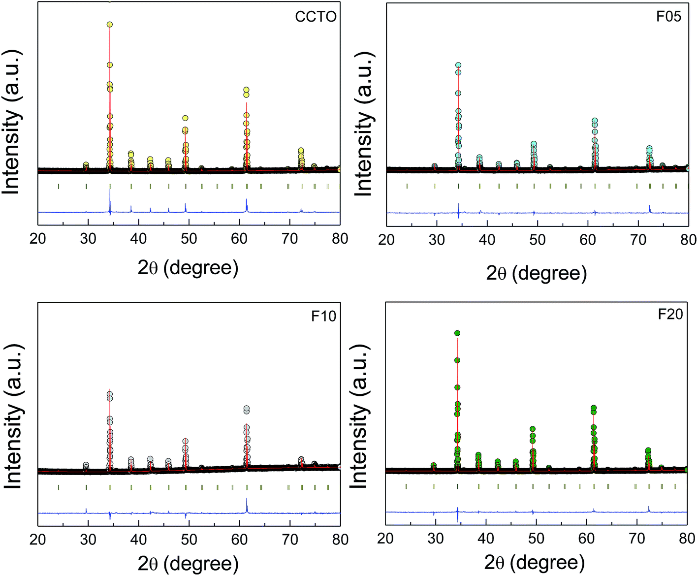 | ||
| Fig. 1 Profile fits for the Rietveld refinements of the XRD patterns of CCTO, F05, F10 and F20 samples. | ||
δ) at RT and 1 kHz, conduction activation energies of the grain (Eg) and grain boundary (Egb), nonlinear coefficient (α) and nonlinear breakdown electric field (Eb)
| Samples | a (Å) | ε′ | tanδ |
Eg | Egb | α | Eb |
|---|---|---|---|---|---|---|---|
| CCTO | 7.393(2) | 23263 |
0.145 | 0.083 | 0.630 | 3.77 | 308.1 |
| F05 | 7.393(9) | 69732 |
0.098 | 0.091 | 0.696 | 3.57 | 345.5 |
| F10 | 7.392(7) | 81306 |
0.077 | 0.091 | 0.714 | 3.58 | 331.5 |
| F20 | 7.393(8) | 98396 |
0.087 | 0.116 | 0.739 | 4.18 | 345.8 |
Surface morphologies of the CCTO and CCTOF ceramics sintered at 1075 °C for 3 h are shown in Fig. 2. As can be clearly seen, there was abnormal grain growth in the microstructure of the CCTO ceramic, where the large sized grains (≈30–50 μm) were surrounded by small grains (≈5–10 μm). This is generally reported in literature and was ascribed to the liquid phase sintering mechanism.14,26,32 It was found that the mean grain size of CCTO ceramics was greatly enlarged by doping with F− anions. Almost all grains of the F05, F10 and F20 samples were very large (≈40–100 μm).
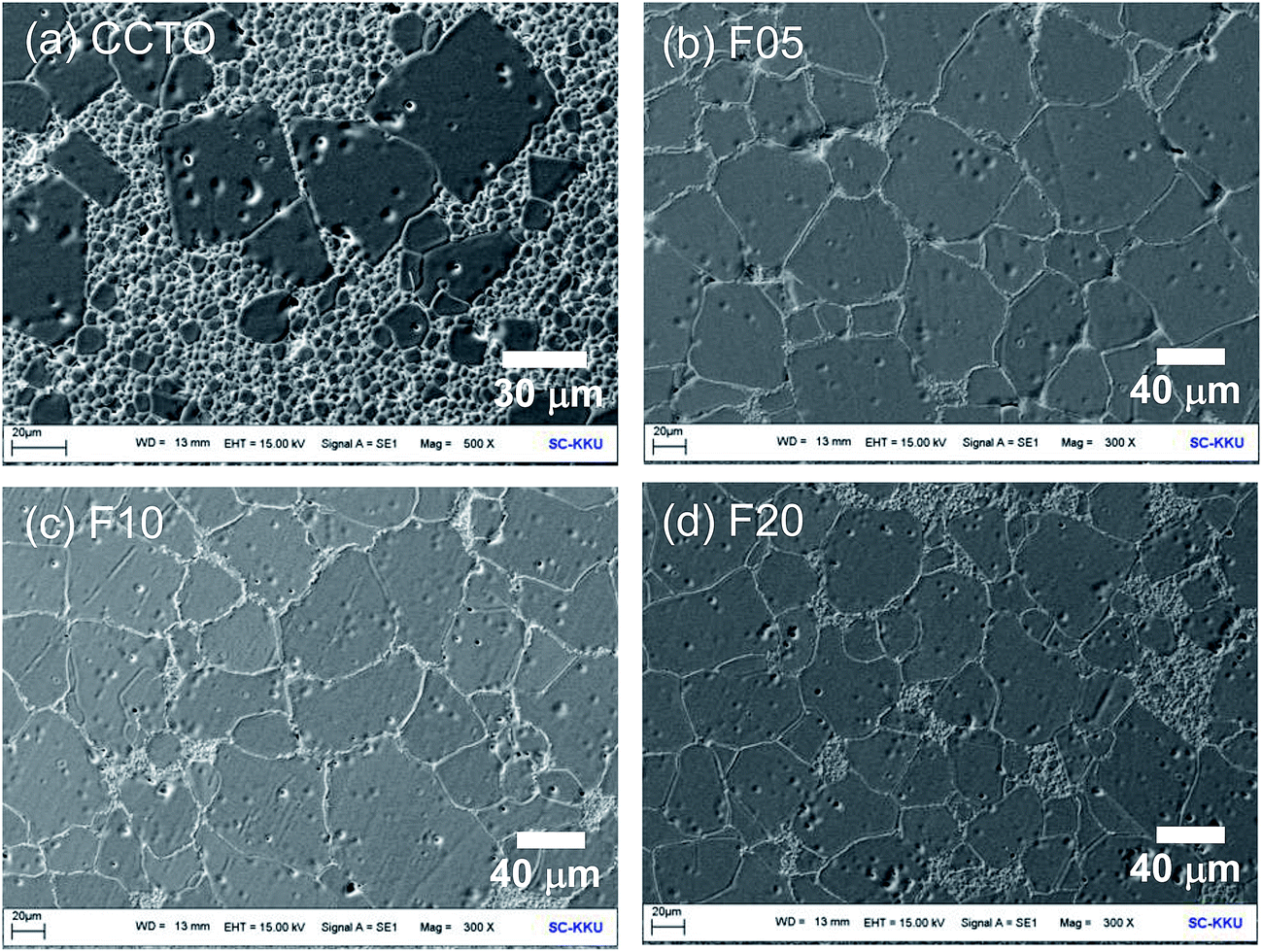 | ||
| Fig. 2 SEM images of polished surfaces of (a) CCTO, (b) F05, (c) F10 and (d) F20 samples. | ||
Usually, the grain growth mechanism of a polycrystalline ceramic is associated with mass transport by diffusion of ions (or atoms) across the GB layer. During sintering, the dopant directly melts and/or reacts with a small part of the major phase to form a eutectic liquid. These can cause a formation of a liquid phase in the microstructure. The liquid was present at the contact areas between the particles in the ceramic microstructure. This can contribute to promotion of the diffusion of ions. For polycrystalline ceramics, a liquid phase generally originates from a eutectic liquid. The eutectic temperature for CuO–TiO2 is about 950 °C for CCTO ceramics.35 Although the liquid phase formed by melting of the dopant usually occurs in metallic systems, it is also possible in CCTOF ceramics. This is due to the low melting point of CuF2 (836 °C). Thus, the formation of a liquid phase is likely caused by these two mechanisms. Enhancement of GB mobility resulted from the presence of the liquid phase(s) and was suggested an important factor for increasing grain growth rate in CCTOF ceramics.
Fig. 3 shows the SEM mapping images of the F05 sample. This result confirms the existence of all major elements (i.e., Ca, Cu, Ti, and O) and confirms the homogeneous dispersion of F− dopant in both of the grains and GBs. Segregation of the F− dopant in any specific region was not seen. In contrast, segregation of Cu was observed along the GBs, which is also generally reported in previous studies.22 This result strongly confirms that the liquid phase is closely associated with a Cu-rich phase, which likely originated from melting of CuF2 and the eutectic phase of CuO–TiO2.
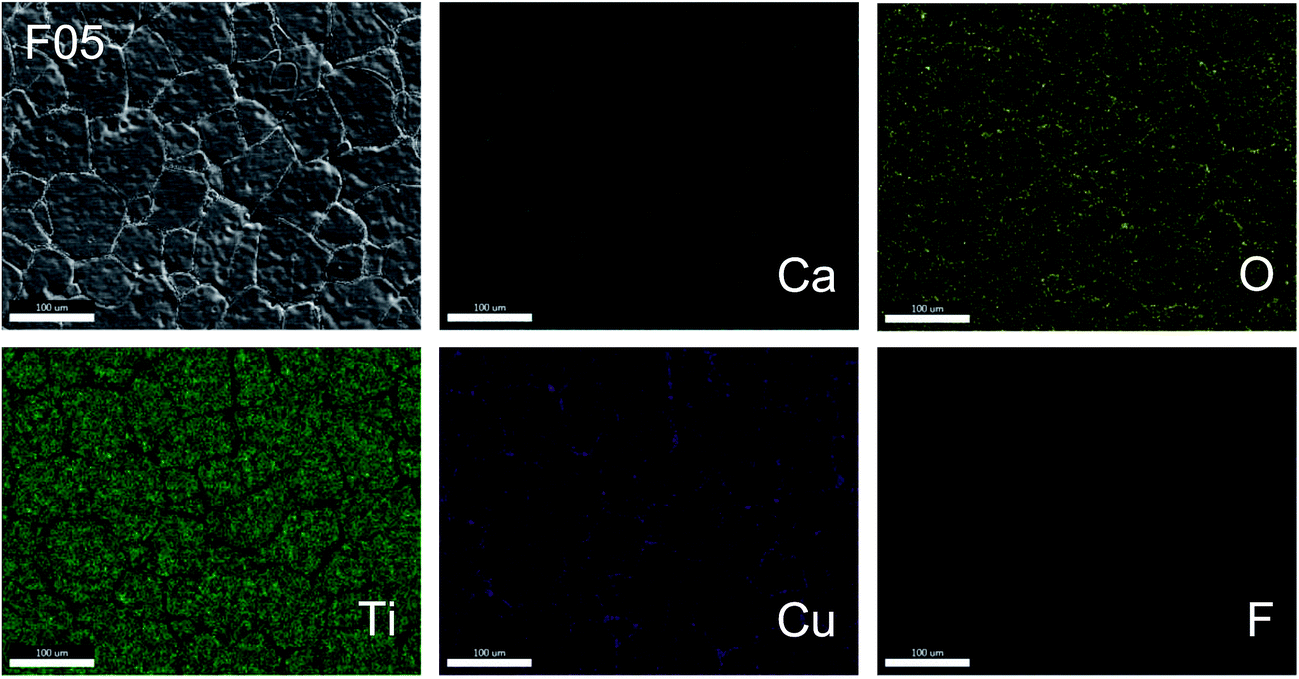 | ||
| Fig. 3 Element mapping of the F05 sample for Ca, Cu, Ti, O and F. | ||
The frequency dependence of the dielectric properties of all the ceramic samples is shown in Fig. 4 ε′ was slightly dependent on frequency in the range of 102 to 105 Hz. Notably, ε′ can be enhanced from ≈104 to ≈105 by doping with F− anions. Considering the microstructural change in CCTOF ceramics, the enlarged grain size is one of the most important parameters that increased ε′. However, the linear and continuous increase in ε′ of the F−-doped CCTO ceramics was not correlated with their grain sizes. ε′ increased with increasing anion dopant concentration, but not for the mean grain sizes. Therefore, variation in ε′ cannot be attributed to the change in the microstructure only. As illustrated in the inset of Fig. 4, a low-frequency tanδ of CCTO ceramics was greatly decreased by doping with F− anions. At 102 Hz, the tanδ of the CCTOF ceramics was reduced by a factor of 5. At frequencies higher than 105 Hz, the frequency dependent behaviors of tanδ for all of the samples were similar, i.e., tanδ increased with increasing frequency. This indicates the dielectric relaxation behavior of primary polarization, which will be discussed below. The ε′ and tanδ values at RT and 1 kHz of all the ceramic samples are summarized in Table 1. It is notable that the low-frequency tanδ of the CCTOF ceramics was significantly reduced to <0.1, while ε′ greatly increased. Generally, this result is hard to achieve in CCTO ceramics because variations in tanδ and ε′ values are usually directly proportional. The ε′ and tanδ values of the CCTO and CCTOF ceramics compared to those reported in literature for both of un-doped and metal ions-doped CCTO ceramics prepared by using different method and sintered under various conditions are shown in Table 2.
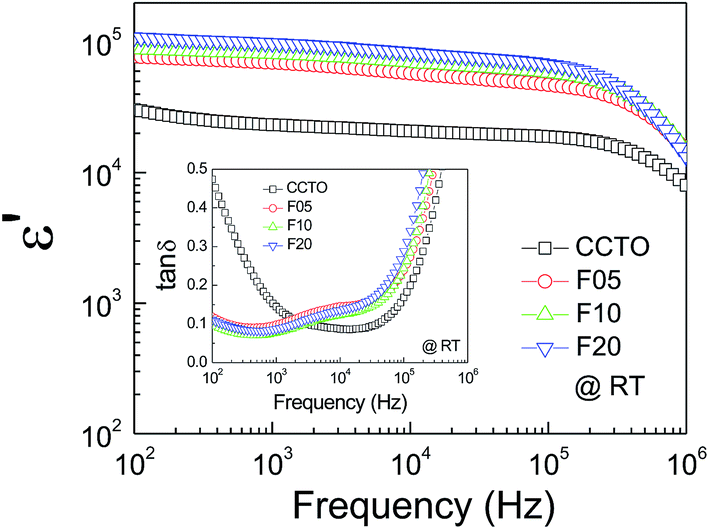 | ||
| Fig. 4 Frequency dependency of dielectric permittivity (ε′) at RT for CCTO, F05, F10 and F20 samples; inset show the loss tangent (tanδ) as a function of frequency at RT. | ||
δ) at RT and 1 kHz of un-doped CCTO and metal ion-doped CCTO ceramics doping with different ions
| Doped-CCTO ceramics (preparation method) | Sintering condition | ε′ | tanδ |
|---|---|---|---|
| Ni-Doped CCTO (SSR method)44 | 1040 °C/4 h | 69833 |
0.073 |
| Sn-Doped CCTO (SSR method)44 | 1040 °C/4 h | 51443 |
0.061 |
| Si-Doped CCTO (SSR method)44 | 1040 °C/4 h | 55240 |
0.136 |
| Al-Doped CCTO (SSR method)44 | 1040 °C/4 h | 30226 |
0.100 |
| Un-doped CCTO (SSR method)44 | 1040 °C/4 h | 45972 |
0.109 |
| Un-doped CCTO (sol–gel method)16 | 1060 °C/48 h | ∼42250 |
∼0.15 |
| Un-doped CCTO (SSR method)17 | 1060 °C/48 h | ∼100000 |
∼1.0 |
| Un-doped CCTO (molten salt method)19 | 1060 °C/1 h | ∼10000 |
∼0.15 |
| 1060 °C/3 h | ∼10000 |
∼0.15 | |
| Un-doped CCTO (SSR method with quenching in water)18 | 1060 °C/3 h | ∼17500 |
∼0.085 |
| Un-doped CCTO (SSR method) [in this work] | 1075 °C for 3 h | 23263 |
0.145 |
| CaCu3Ti4O11.9F0.10 (SSR method) [in this work] | 1075 °C for 3 h | 81306 |
0.077 |
The dielectric relaxation behavior of CCTO and CCTOF ceramics was studied. As shown in Fig. 5, two dielectric relaxations were observed in distinct frequency ranges. The low-frequency dielectric relaxation likely originated from the sample-electrode effect.41 The relatively high-frequency dielectric relaxation (i.e., the primary relaxation) has widely been accepted as associated with the IBLC effect, i.e., the Maxwell–Wagner polarization relaxation.13,21 The step-like decrease in ε′ and relaxation peak of ε′′ (ε′′ is the imaginary part of the complex dielectric permittivity or dielectric loss, ε′′ = ε′ × tanδ) shifted to a higher frequency with increasing temperature, indicating a thermally activated relaxation mechanism. The activation energy for dielectric relaxation can be calculated from the critical frequency (fmax) at various temperatures at which the relaxation peak appeared as:
 | (2) |
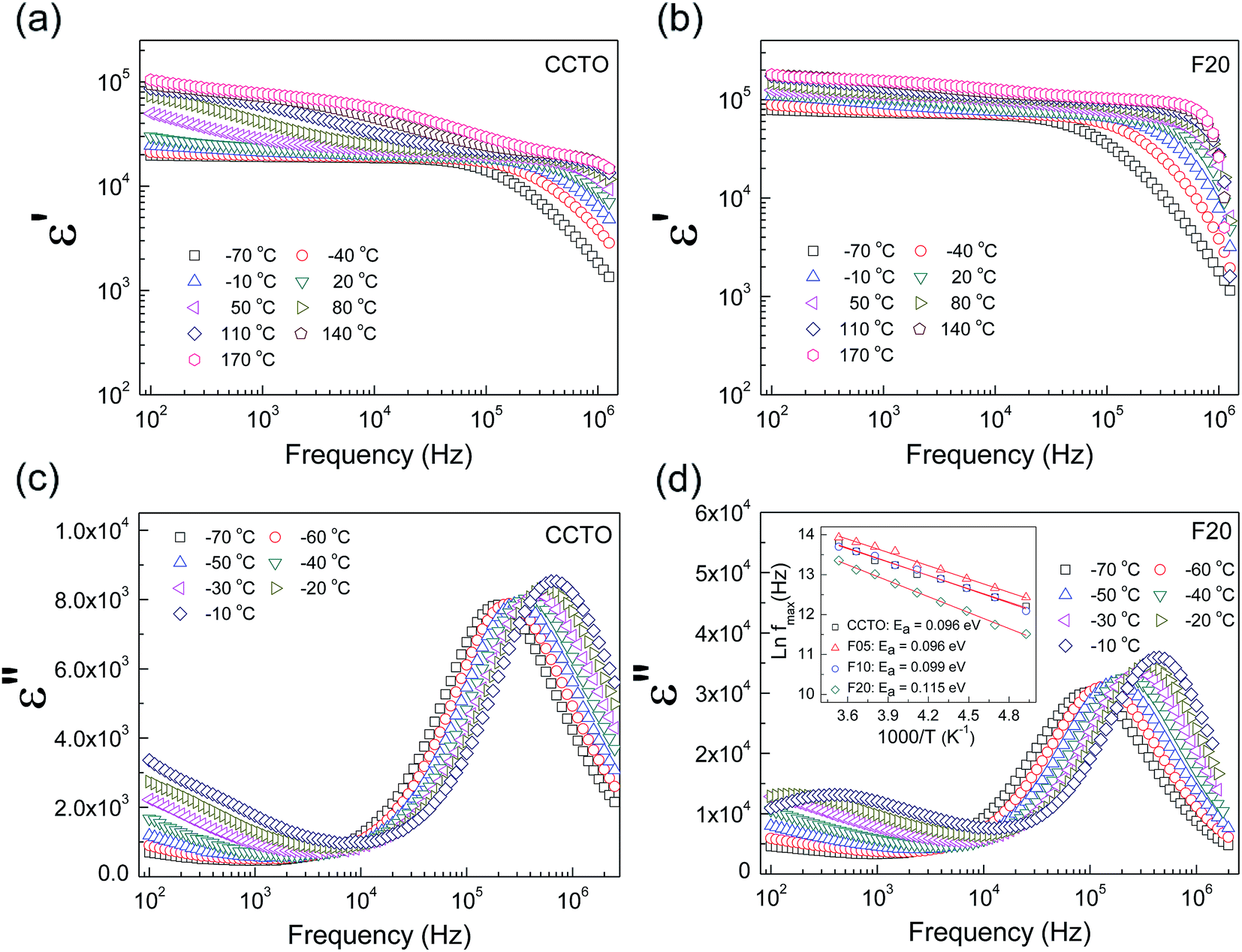 | ||
| Fig. 5 Frequency dependencies of dielectric permittivity (ε′) and dielectric loss (ε′′) at various temperatures for (a, c) CCTO and (b, d) F20 samples; inset of (d) shows Arrhenius plots of fmax for the dielectric relation. | ||
To elucidate the influences of F− anion dopant ions on the dielectric properties of CCTO ceramics, the grain and GB responses were studied using an impedance spectroscopy technique. Fig. 6(a) and (b) show Z* plots for all the samples at RT and 80 °C, respectively. Only the linear part of the semicircular arcs was observed at RT in the frequency range of 102 to 106 Hz. A nonzero intercept on the Z′ axis was observed, inset of Fig. 6(a), indicating an electrical response of the semiconducting grains.42,43 Thus, the linear part of the semicircular arcs should be due to the electrical response of the GBs. The grain resistance (Rg) values (estimated from the nonzero intercept) of the CCTOF ceramics were smaller than that of the undoped CCTO ceramic by a factor of 2. At RT, Rg of the CCTO sample was ≈100 Ω cm, while Rg values of the CCTOF ceramics were nearly the same in value with Rg ≈ 50 Ω cm. At RT, it is very difficult (or perhaps impossible) to accurately calculate the value of Rgb in the measured frequency range since just few data points on the full arcs appeared in these Z* plots. The trend of Rgb values for the CCTOF ceramics cannot be determined. To obtain this, a Z* plot at a high temperature should be performed. In Fig. 7(b), the Rgb of each sample was estimated and found to be significantly increased by doping with F−. Rgb of the CCTOF ceramics was enhanced even through the mean grain size increased compared to that of the CCTO sample. This result gives a significant clue, reflecting the largely enhanced resistance of individual GB layers. This is one of the most important factors contributing to reduction in a low-frequency tanδ in CCTOF ceramics [inset of Fig. 4]. Thus, the distribution of dopants near GBs can cause an increase in the GB resistivity, which often make great influence on the low-frequency dielectric properties,44 as clearly seen in Fig. 5. It is worth noting that all the samples were electrically heterogeneous, consisting of grains with very small Rg values and very high values of Rgb. Therefore, it is reasonable to suggest that the giant dielectric response in CCTOF ceramics originated from the IBLC effect.
 | ||
| Fig. 6 (a and b) Impedance complex plane (Z*) plots of CCTO, F05, F10 and F20 samples at room temperature and 80 °C, respectively; inset of (a) shows an expanded view of high frequency Z* plots at RT, revealing the nonzero intercept on Z′ axis. (c and d) Arrhenius plots of σg and σgb, respectively. | ||
 | ||
| Fig. 7 XPS spectra of CCTO and F10 samples: (a, c) Ti 2p regions and (b, d) Cu 2p regions. | ||
Rg and Rgb values can be calculated in various temperatures. The conductivities of the grain (σg) and GB (σgb) were calculated from Rg and Rgb, respectively. As demonstrated in Fig. 6(c) and (d), the temperature dependencies of σg and σgb follow the Arrhenius law:
 | (3) |
 | (4) |
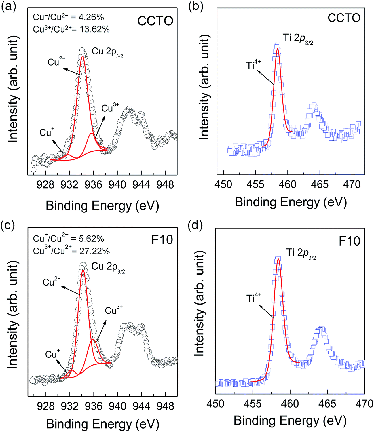
As shown in the inset of Fig. 6(a), Rg of CCTO ceramics was reduced by doping with F− anions, indicating an increase in the concentration of free charge carriers in the grain interiors. To clarify the effect of F− doping on the electrical properties of the grains, variation in valence states of Cu2+ and Ti4+ ions in CCTO and CCTOF samples was investigated using XPS and XANES techniques. As illustrated in Fig. 7(a) and (c), the main XPS peaks at ≈933 eV for the CCTO and F10 samples confirm the existence of large numbers of Cu2+ ions.9,28,32 The Cu 2p3/2 region can be divided into three peaks using Gaussian–Lorentzian profile fitting. The small XPS peaks at relatively lower and higher binding energies at ≈931 and ≈936 eV indicated the existence of Cu+ and Cu3+, respectively.9,28,32 The Cu+/Cu2+ ratios of the CCTO and F10 samples were, respectively, about 4.26% and 5.65%, while their respective Cu3+/Cu2+ ratios were 13.62% and 27.22%. Doping CCTO with F− caused an increase in both Cu+ and Cu3+ concentrations.
In addition to Cu+ and Cu3+, the presence of Ti3+ ions is usually considered a major cause of the formation of n-type semiconducting grains in CCTO ceramics. As depicted in Fig. 7(b) and (d), the primary XPS peak at ≈458 eV for Ti4+ was confirmed in all the samples. Unfortunately, the presence of Ti3+ cannot be modeled using Gaussian–Lorentzian profile fitting. This may be due to a small amount of Ti3+ in both the samples.2 Thus, XANES was used to further investigate to the existence of Ti3+. Fig. 8 shows normalized Ti K-edge XANES spectra of the CCTO and F10 samples as well as the standard TiO2 (Ti4+) and Ti2O3 (Ti3+) samples. It was found that the position of the edge energy of both samples was very close to the TiO2 standard. As expected, a small amount of Ti3+ was confirmed to exist. To obtain the ratios of Ti3+/Ti4+, the edge value was calculated from the maximum value of the first derivative in the edge region.15 The ratio of Ti3+/Ti4+ can be calculated from the energy edge value.39 The ratios of Ti3+/Ti4+ in the CCTO and F10 samples were found to be 0.82% and 2.46%, respectively.
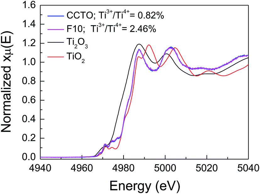 | ||
| Fig. 8 Normalized X-ray absorption near edge structure (XANES) spectra for Ti K-edge of the CCTO and F10 samples. | ||
Substitution of O2− with F− anions requires charge compensation, which can be achieved by reduction in cation valence (Cu2+ → Cu+ and Ti4+ → Ti3+). This charge compensation behavior is similar to that observed in the case of Y3+ doped-CCTO ceramics, which Rg of CCTO was reduced by doping with Y3+.45,46 It is worth noting that the Cu3+/Cu2+ ratio of the F10 sample was significantly increased. As shown in the SEM-mapping image for Cu dispersion, Fig. 3, segregation of Cu-rich phase along the GBs was observed. This indicated the decomposition of CuO from the CCTO lattice, creating cation vacancies. Therefore, it is possible that the increased Cu3+/Cu2+ ratio of the F10 sample might be due to the creation of Cu vacancies.9
Generally, the conductivity of n-type semiconducting grains is elevated by increasing the number of free electrons. Thus, the reduction in Rg of the CCTOF samples should be correlated with the increase in Cu+/Cu2+ and Ti3+/Ti4+ ratios over those found in the CCTO sample. For p-type semiconductor CuO ceramics, conduction is primarily caused by hole hopping between Cu3+ ↔ Cu2+. The increase in the Cu3+/Cu2+ ratio may also be an important cause of the reduced Rg. Form this point of view, hopping of charge carriers between Cu+ ↔ Cu2+, Cu3+ ↔ Cu2+, and Ti3+ ↔ Ti4+ sites in the CCTO structure can result in electrical conductivity. According to our previous report, we found that the variation in Rg of Na0.5Y0.5Cu3Ti4O12 ceramics was only consistent with a change in the Ti3+/Ti4+ ratio, whereas changes in Cu+/Cu2+ and Cu3+/Cu2+ ratios was not correlated to Rg values.47 The conduction mechanism inside the n-type semiconducting grains might be primarily attributed to electron hopping from a Ti3+–O–Ti4+ to a Ti4+–O–Ti3+. Hopping of charge carriers between complex defects, i.e., Cu+–O–Cu2+ ↔ Cu2+–O–Cu3+, was likely difficult owing to much different valance states of Cu+ and Cu3+.
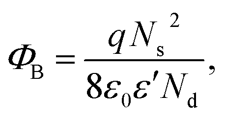
The effect of F− anions on the non-ohmic properties of CCTO ceramics is illustrated in Fig. 9. All the samples exhibited nonlinear J–E characteristics. Accordingly, Eb and α values were calculated and summarized in Table 1. According to the improved dielectric properties and the observed nonlinear electrical properties of CCTOF ceramics, it was suggested that the sample could be applied as capacitor-varistors.48 α values for all the samples were not significantly different, while Eb values of the CCTOF samples were greater than that of the undoped CCTO sample, even though their grain sizes were larger than those of the CCTO sample. The volume fraction of the GB, which is inversely proportional to its mean grain size, was decreased by doping with F− anions. The increase in Eb of the CCTOF samples was consistent with their enhanced Rgb values over that of the CCTO sample. Although the volume fraction of the GB in the CCTOF samples was lower than that of the CCTO sample, the total resistance of their GBs (Rgb) and Eb were larger. Thus, the resistivity of an individual GB layer of the CCTOF samples should much be larger than that of the CCTO sample. These results indicate that the intrinsic property (i.e., potential barrier height) of the GB of CCTO ceramics was enhanced by F− doping. It was reasonably proposed that based on the n-type semiconducting grains of CCTO ceramics, the electronic energy band structure across the GB layer was equivalent to n–i–n.20,49 Double Schottky potential barriers can be created at interfaces between n-type grains caused by trapping at acceptor states. This resulted in the bending of the conduction band across the GB. A potential barrier (ΦB) was created at the GB sandwiched by n-type semiconducting grains.20 In the absence of a DC bias, ΦB can be expressed as:
 | (5) |
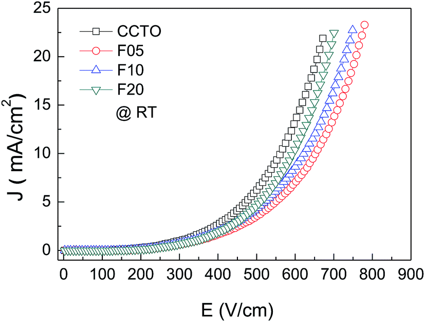 | ||
| Fig. 9 Nonlinear current density–electric field (J–E) characteristics at RT of CCTO, F05, F10 and F20 samples. | ||
Substitution of F− anions into CCTO ceramics can simultaneously improve the electrical properties of the grains and GBs. These can cause increases in both of the free charge carrier concentration inside the semiconducting grains and Schottky barrier height at the GBs, respectively. Under an applied electric field, more charges accumulated at the interface between the semiconducting grain and GB layer due to a high concentration of free charges inside the grain producing a stronger intensity of interfacial polarization (Maxwell–Wagner polarization). This gave rise to a large increase in ε′. Enhanced ΦB resulting in Rgb is the major cause the reduced low-frequency tanδ.
4. Conclusions
Significantly improved giant dielectric properties of CCTO ceramics via simultaneously tuning the electric properties of the grains and GBs was successfully done by doping CCTO with F− anions. The grain size of CCTO ceramics was thus enlarged. The low-frequency tanδ of F−-doped CCTO ceramics was greatly reduced by a factor of 5 compared to that of the undoped CCTO ceramic, which was attributed to a large increase in Rgb and potential barrier height at the GBs. These results were confirmed by the slight increase in electric breakdown strength of F−-doped CCTO ceramics, even though the mean grain size was greatly increased. According to the XPS and XANES results, it was shown that the charge carrier concentration inside the semiconducting grains of F−-doped CCTO ceramics was increased corresponding to the observed reduction in Rg. This was responsible for the observed increase in ε′ from ≈104 to ≈105 at 1 kHz due to the increased intensity of interfacial polarization at the GBs. Maxwell–Wagner polarization relaxation based on the internal barrier layer capacitor model of Schottky barriers at the GBs can be used to clearly explain the variations of the giant dielectric behavior and nonlinear electrical properties of F−-doped CCTO ceramics.
Acknowledgements
This work was financially supported by the Thailand Research Fund (TRF) and Khon Kaen University (Contract No. RSA5880012) and under the TRF Senior Research Scholar (Contract No. RTA5780004). The authors would like to thank the Synchrotron Light Research Institute (BL5.2) (Public Organization), Nakhon Ratchasima, Thailand for XANES measurements and the SUT-NANOTEC-SLRI Joint Research Facility for XPS facility. J. Jumpatam thanks the Thailand Research Fund under The Royal Golden Jubilee Ph.D. Program [Grant number PHD/0079/2557] for his Ph.D. scholarship.References
- C. C. Homes, T. Vogt, S. M. Shapiro, S. Wakimoto and A. P. Ramirez, Science, 2001, 293, 673–676 CrossRef CAS PubMed.
- W. Hu, Y. Liu, R. L. Withers, T. J. Frankcombe, L. Norén, A. Snashall, M. Kitchin, P. Smith, B. Gong, H. Chen, J. Schiemer, F. Brink and J. Wong-Leung, Nat. Mater., 2013, 12, 821–826 CrossRef CAS PubMed.
- G. Liu, H. Fan, J. Xu, Z. Liu and Y. Zhao, RSC Adv., 2016, 6, 48708–48714 RSC.
- W. Tuichai, S. Danwittayakul, S. Maensiri and P. Thongbai, RSC Adv., 2016, 6, 5582–5589 RSC.
- A. O. Turky, M. M. Rashad, Z. I. Zaki, I. A. Ibrahim and M. Bechelany, RSC Adv., 2015, 5, 18767–18772 RSC.
- M. A. Subramanian, D. Li, N. Duan, B. A. Reisner and A. W. Sleight, J. Solid State Chem., 2000, 151, 323–325 CrossRef CAS.
- B. Shri Prakash and K. B. R. Varma, J. Mater. Sci.: Mater. Electron., 2006, 17, 899–907 CrossRef CAS.
- S.-H. Hong, D.-Y. Kim, H.-M. Park and Y.-M. Kim, J. Am. Ceram. Soc., 2007, 90, 2118–2121 CrossRef CAS.
- M. Li, G. Cai, D. F. Zhang, W. Y. Wang, W. J. Wang and X. L. Chen, J. Appl. Phys., 2008, 104, 074107 CrossRef.
- L. Liu, H. Fan, P. Fang and X. Chen, Mater. Res. Bull., 2008, 43, 1800–1807 CrossRef CAS.
- L. Ni, X. M. Chen and X. Q. Liu, Mater. Chem. Phys., 2010, 124, 982–986 CrossRef CAS.
- P. Thongbai, J. Jumpatam, T. Yamwong and S. Maensiri, J. Eur. Ceram. Soc., 2012, 32, 2423–2430 CrossRef CAS.
- P. Thongbai, J. Jumpatam, B. Putasaeng, T. Yamwong and S. Maensiri, J. Appl. Phys., 2012, 112, 114115 CrossRef.
- J. Jumpatam, B. Putasaeng, T. Yamwong, P. Thongbai and S. Maensiri, Ceram. Int., 2013, 39, 1057–1064 CrossRef CAS.
- J. Boonlakhorn and P. Thongbai, J. Electron. Mater., 2015, 44, 3687–3695 CrossRef CAS.
- L. Liu, H. Fan, P. Fang and L. Jin, Solid State Commun., 2007, 142, 573–576 CrossRef CAS.
- L. Liu, H. Fan, X. Chen and P. Fang, J. Alloys Compd., 2009, 469, 529–534 CrossRef CAS.
- L. Liu, D. Shi, S. Zheng, Y. Huang, S. Wu, Y. Li, L. Fang and C. Hu, Mater. Chem. Phys., 2013, 139, 844–850 CrossRef CAS.
- Y. Huang, L. Liu, D. Shi, S. Wu, S. Zheng, L. Fang, C. Hu and B. Elouadi, Ceram. Int., 2013, 39, 6063–6068 CrossRef CAS.
- T. Adams, D. Sinclair and A. West, Phys. Rev. B: Condens. Matter Mater. Phys., 2006, 73, 094124 CrossRef.
- J. Liu, C.-G. Duan, W.-G. Yin, W. Mei, R. Smith and J. Hardy, Phys. Rev. B: Condens. Matter Mater. Phys., 2004, 70, 144106 CrossRef.
- R. Schmidt, M. C. Stennett, N. C. Hyatt, J. Pokorny, J. Prado-Gonjal, M. Li and D. C. Sinclair, J. Eur. Ceram. Soc., 2012, 32, 3313–3323 CrossRef CAS.
- Z. Yang, L. Zhang, X. Chao, L. Xiong and J. Liu, J. Alloys Compd., 2011, 509, 8716–8719 CrossRef CAS.
- S.-Y. Chung, I.-D. Kim and S.-J. L. Kang, Nat. Mater., 2004, 3, 774–778 CrossRef CAS PubMed.
- M. A. Ramírez, P. R. Bueno, J. A. Varela and E. Longo, Appl. Phys. Lett., 2006, 89, 212102 CrossRef.
- J. Boonlakhorn, P. Kidkhunthod and P. Thongbai, J. Eur. Ceram. Soc., 2015, 35, 3521–3528 CrossRef CAS.
- L. Sun, R. Zhang, Z. Wang, E. Cao, Y. Zhang and L. Ju, RSC Adv., 2016, 6, 55984–55989 RSC.
- L. Ni and X. M. Chen, Solid State Commun., 2009, 149, 379–383 CrossRef CAS.
- A. Nautiyal, C. Autret, C. Honstettre, S. De Almeida-Didry, M. El Amrani, S. Roger, B. Negulescu and A. Ruyter, J. Eur. Ceram. Soc., 2016, 36, 1391–1398 CrossRef CAS.
- M. F. Ab Rahman, S. D. Hutagalung, Z. A. Ahmad, M. F. Ain and J. J. Mohamed, J. Mater. Sci.: Mater. Electron., 2015, 26, 3947–3956 CrossRef CAS.
- L. Singh, I. W. Kim, B. C. Sin, K. D. Mandal, U. S. Rai, A. Ullah, H. Chung and Y. Lee, RSC Adv., 2014, 4, 52770–52784 RSC.
- L. Ni and X. M. Chen, J. Am. Ceram. Soc., 2010, 93, 184–189 CrossRef CAS.
- W. L. Li, Y. Zhao, Q. G. Chi, Z. G. Zhang and W. D. Fei, RSC Adv., 2012, 2, 6073 RSC.
- M. Gao, D. Feng, G. Yao, Y. Zhang, C. L. Chen and Y. Lin, RSC Adv., 2015, 5, 92958–92962 RSC.
- L. Singh, B. C. Sin, I. W. Kim, K. D. Mandal, H. Chung, Y. Lee and J. Varela, J. Am. Ceram. Soc., 2016, 99, 27–34 CrossRef CAS.
- J. Boonlakhorn and P. Thongbai, Jpn. J. Appl. Phys., 2015, 54, 06FJ06 CrossRef.
- R. Yu, H. Xue, Z. Cao, L. Chen and Z. Xiong, J. Eur. Ceram. Soc., 2012, 32, 1245–1249 CrossRef CAS.
- A. E. Smith, T. G. Calvarese, A. W. Sleight and M. A. Subramanian, J. Solid State Chem., 2009, 182, 409–411 CrossRef CAS.
- M. Newville, J. Synchrotron Radiat., 2001, 8, 96–100 CrossRef CAS PubMed.
- R. D. Shannon, Acta Crystallogr., Sect. A: Cryst. Phys., Diffr., Theor. Gen. Crystallogr., 1976, 32, 751–767 CrossRef.
- M. Li, Z. Shen, M. Nygren, A. Feteira, D. C. Sinclair and A. R. West, J. Appl. Phys., 2009, 106, 104106 CrossRef.
- S. I. R. Costa, M. Li, J. R. Frade and D. C. Sinclair, RSC Adv., 2013, 3, 7030–7036 RSC.
- R. Schmidt, S. Pandey, P. Fiorenza and D. C. Sinclair, RSC Adv., 2013, 3, 14580–14589 RSC.
- L. Liu, Y. Huang, Y. Li, D. Shi, S. Zheng, S. Wu, L. Fang and C. Hu, J. Mater. Sci., 2012, 47, 2294–2299 CrossRef CAS.
- J. Deng, X. Sun, S. Liu, L. Liu, T. Yan, L. Fang and B. Elouadi, J. Adv. Dielectr., 2016, 06, 1650009 CrossRef CAS.
- G. Li, Z. Chen, X. Sun, L. Liu, L. Fang and B. Elouadi, Mater. Res. Bull., 2015, 65, 260–265 CrossRef CAS.
- J. Jumpatam, A. Mooltang, B. Putasaeng, P. Kidkhunthod, N. Chanlek, P. Thongbai and S. Maensiri, Ceram. Int., 2016, 42, 16287–16295 CrossRef CAS.
- Y. Huang, D. Shi, Y. Li, G. Li, Q. Wang, L. Liu and L. Fang, J. Mater. Sci.: Mater. Electron., 2012, 24, 1994–1999 CrossRef.
- L. Liu, L. Fang, Y. Huang, Y. Li, D. Shi, S. Zheng, S. Wu and C. Hu, J. Appl. Phys., 2011, 110, 094101 CrossRef.
- M. Li and D. C. Sinclair, J. Appl. Phys., 2013, 114, 034106 CrossRef.
| This journal is © The Royal Society of Chemistry 2017 |