
 Open Access Article
 This Open Access Article is licensed under a Creative Commons Attribution-Non Commercial 3.0 Unported Licence
Seeds triggered massive synthesis and multi-step room temperature post-processing of silver nanoink—application for paper electronics†
Xiao-Yang Zhangabc,
Jia-Jia Xuac,
Jing-Yuan Wuac,
Feng Shanac,
Xiao-Dan Maa,
Yu-Zhang Chena and
Tong Zhang*abc
aJoint International Research Laboratory of Information Display and Visualization, School of Electronic Science and Engineering, Southeast University, Nanjing, 210096, People's Republic of China. E-mail: tzhang@seu.edu.cn
bKey Laboratory of Micro-Inertial Instrument and Advanced Navigation Technology, Ministry of Education, School of Instrument Science and Engineering, Southeast University, Nanjing, 210096, People's Republic of China
cSuzhou Key Laboratory of Metal Nano-Optoelectronic Technology, Suzhou Research Institute of Southeast University, Suzhou, 215123, People's Republic of China
First published on 22nd December 2016
Abstract
Paper electronics based on ink-jet printing has become a promising technology for building new concepts of flexible and three dimensional (3D) electronic circuits and devices in a simple, cost-effective and untraditional way. In this paper, we focus on the development of massive silver nanoink syntheses and room temperature post-processing methods to meet the particular technical features of paper electronics. We firstly proposed a seed triggered synthesis method to achieve uniform silver nanoparticles without the existence of large nanostructures. Such a silver nanoparticle solution can be easily centrifuged to nanoink at a relatively low speed. Then we showed that the electric conductivities of the printed silver tracks can be improved significantly by a multi-step room temperature post-processing (MRTP) method including organic solution washing, white LED irradiation and electroless deposition in sequence. Conductivities of up to 17% of that of bulk silver can be achieved which is nearly 2 times that of the printed silver tracks treated by a conventional heating process at 120 °C for a long time. Moreover, by combining together with 3D paper folding art, we systematically investigated the electrical performances of the printed circuits associated with the printing uniformity, mechanical flexibility and strain sensitivity. These overall characteristics of the room temperature treated printing technology show great potential for the development of innovative 3D electronic products in the future.
Introduction
Ink-jet printing, as a drop-on-demand method, has gained much attention as an alternative to conversional photolithography for the fabrication of flexible electronic circuits and devices. It has shown great potential applications in various fields such as displays, solar cells, and sensing.1–6 Paper, as one of the flexible substrates used, has shown its popularity in electronic circuit fabrication because of its inexpensive nature, biodegradability, and light weight.7–12 The concept of paper electronics, as a complete subversion of traditional fabrication techniques of electronic devices, may bring about a new technology revolution in the electronics industry in the near future.Currently, there are two main challenges in the field of ink-jet printing, especially for paper based electronic applications. The first one is the development of highly reliable fabrication methods of conductive inks. Among various conductive inks, silver nanoink is the best candidate because of its high conductivity, relatively low cost and oxidation resistance.13–17 Different from conventional optical applications focusing on the accurate control of their shape and optical characteristics, the requirements of silver nanoparticle synthesis methods for ink-jet printing can be categorized as two parts. (a) How to obtain a large amount of nanoparticles without micrometer-sized large crystals and aggregations.18–20 It is a critical factor to enhance the cost control and promote the industrialization of ink-jet printing, however, still difficult to realize. It is because the mainstream strategy of silver nanoparticle synthesis is the seed control at the initial reaction stage.21,22 Such methods are effective to obtain nanostructures with well controlled shapes and sizes in small batch. However, the particle yields of these methods are easily declined by many factors such as the reaction temperature fluctuation, ambient humidity and chemical purity which may strongly influence the crystal types and the amount of the seeds at the initial stage. Therefore, once the reaction is extended to gram level, by-products such as various large crystals and nanowires are usually difficult to eliminate. (b) How to purify the original nanoparticle solution in the ink preparation step using an easy way. Currently, since large crystal and aggregations are difficult to avoid in the synthesis, most of the as-synthesized solutions need to be filtered before using as inks.16,19,20 Moreover, the silver nanoparticle solutions with high amounts of capping agents and helpers used for shape and size control are difficult to wash unless very high centrifugation speeds, usually over 10![[thin space (1/6-em)]](https://www.rsc.org/images/entities/char_2009.gif) 000 rpm are used. These complicated treatment processes result in high time and money cost to obtain silver ink with high solid content. Therefore, new particle synthesis methods suitable for large-quantity production and easy purified process are highly required.
000 rpm are used. These complicated treatment processes result in high time and money cost to obtain silver ink with high solid content. Therefore, new particle synthesis methods suitable for large-quantity production and easy purified process are highly required.
Post-processing of the ink-jet printed silver tracks is another focused critical technology for paper-based electronics.23 Most commonly used method is thermal sintering which prompts the coalescence of silver nanoparticles by high-temperature heating. It is because that the shells consisted of stabilizers and capping agents between the adjacent nanoparticles can be removed thermally.24 However, such high-temperature treatment could also cause massive damage to flexible substrates, especially papers, because of their sensitivity to heat. Therefore, low-temperature nanoparticle joining methods have been invented to meet the requirements of paper electronics. These technologies, mainly applied in electronic packaging,25–29 are aimed to remove the shells of nanoparticles by various methods in a relative low temperature way. Obviously, innovative post-processing methods of printed silver tracks at low temperature, or even at room temperature, are highly desirable technique18,30–33 for the development of paper electronics.
In the present work, we firstly proposed a highly reliable synthesis strategy to improve the yield of silver nanoparticles and avoid the formation of large crystal structures. Different from conventional synthesis strategies focusing on the initial stage of seed control, we used hydrogen peroxide (H2O2) to etch all the initial seeds and then trigger the crystal growth process by adding new seeds. This synthesis strategy reduces the requirements of the reaction condition and is suitable for massive production of silver ink. Next we exhibited that the conductivities of the printed silver tracks can be improved to over 17% of that of bulk silver at room temperature. This conductivity is near two times of that of the printed silver tracks treated by conventional thermal sintering process. The proposed multistep room-temperature post-processing (MRTP) method integrated various techniques including organic solvent washing, white light emitting diode (LED) based photonic sintering and electroless deposition. This post-processing method avoids the thermal damage of the substrates, promotes the joining of nanoparticles and enhances the compactness of the silver tracks. Finally, we demonstrated the application of the paper based electronic circuits for new concept three-dimensional (3D) flexible electronics and systematically explored the uniformity of the printed circuits and their mechanical flexibility during bending.
Experimental section
Chemicals
Silver nitrate (AgNO3, 99.9%), polyvinyl pyrrolidone (PVP, molecular weight 29000), sodium chloride (NaCl, 99.9%), and sodium citrate (99.9%) were purchased from Sigma-Aldrich. Hydrazine hydrate (99.5%) was purchased from Hujiang Co., Ltd. Chloroauric acid (99%) was purchased from Sinopharm Chemical Reagent Co., Ltd. All materials were used as received without further purification. In all experiments, ultra-pure water (18.4 MΩ cm) was used.
Silver nanoparticles synthesis and ink formulation
The synthesis process includes ethylene glycol (EG) reflux, initial nucleus etching, seeds triggered nucleation and crystal structure growth as illustrated in Fig. 1, the second line. In the first stage, 4.5 g AgNO3 was dissolved in 50 mL EG at room temperature. Meanwhile, 1 g PVP and 0.012 g NaCl were dissolved in 450 mL EG and the solution was heated at 145 °C for 1.5 h with continuous stirring. In the second stage, the AgNO3 solution was added into resultant solution under drastic stirring, and about 13 mL H2O2 was added in sequence immediately. Then the solution was heated up to 170 °C. In the third stage, 40 mL gold seed solution prepared using a reported method34 was added. Finally, the solution was heated up to 200 °C for about 0.5 h, and then the temperature was decreased to room temperature. Silver nanoparticle solution was obtained as shown in Fig. 2. Note that as the reaction temperature was high, and large amounts of chemicals were added in a relative short time, condenser was needed in the reaction to cool down the vapor rapidly, and the reaction flask should be well ventilated to keep a safety pressure. | ||
| Fig. 1 Schematically strategy comparison between (a) conventional seed control method and (b) the present seeds triggered synthesis method of silver nanoparticles. | ||
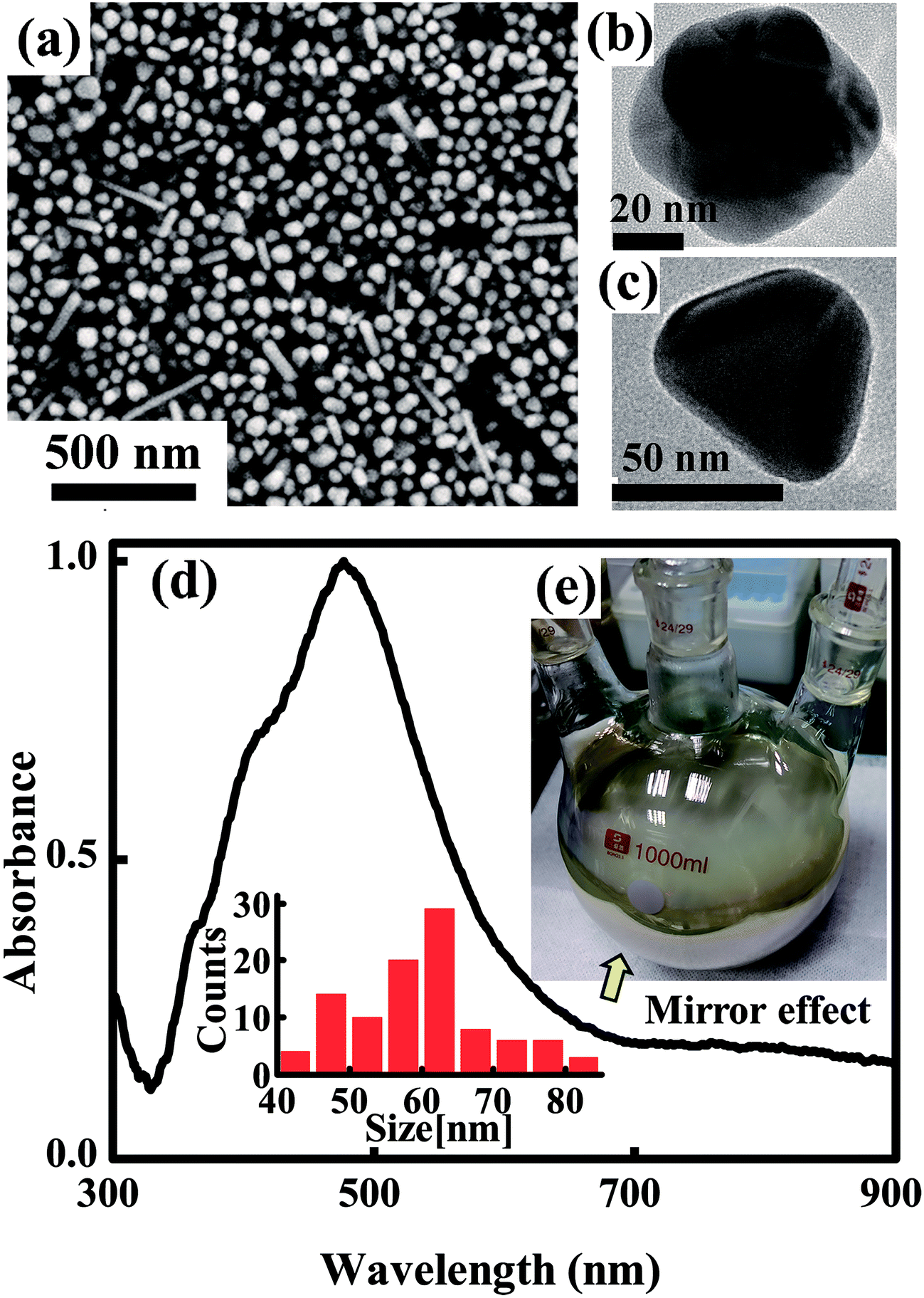 | ||
| Fig. 2 (a) SEM image of the synthesized silver nanoparticle. (b and c) High resolution TEM images of isolated silver nanoparticles. (d) UV-vis absorbance spectrum of silver nanoparticles and the histograms of particle size distributions. (e) Optical photograph of the as-prepared silver nanoparticles solution. | ||
For the ink preparation, the as-synthesized silver nanoparticles were washed three times by centrifugation at 9000 rpm for 20–30 min using ethanol. Then EG was added to adjust the viscosity of ink. Volume ratio between ethanol and EG was 3:2 in the ink with a solid content of ∼15%.
Steps of ink-jet printing and post-processing
Paper based silver patterns and tracks were printed using Epson R270 ink-jet printer on photo papers. The printing process can be repeated several times to increase the thickness of the tracks. The relation between the thickness of the tracks and the printing cycles is shown in Fig. S1, ESI.† The printed samples were then treated by MRTP as illustrated in Fig. 3. It contains two steps: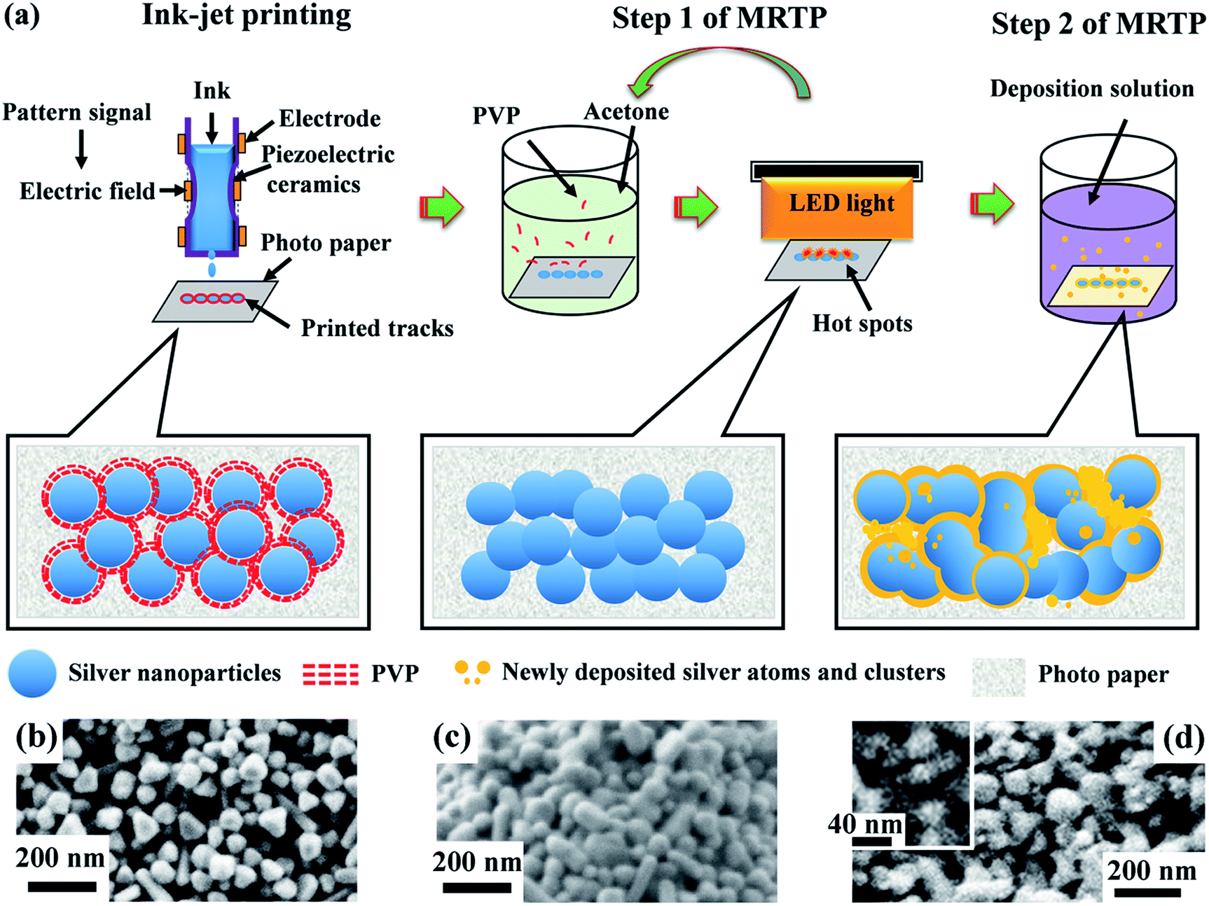 | ||
| Fig. 3 (a) Schematic representation of MRTP. SEM images show the morphologies of the silver tracks at different steps. (b) Before sintering, (c) treated by the Step 1 of MRTP and (d) treated by Step 2 of MRTP. The inset in (d) shows the high resolution image of small nanoparticles newly deposited on to the silver track. | ||
Step 1. Acetone assisted photonic sintering. The printed samples were immerged in acetone solvent for 10 min, and then dried out. After that, they were illuminated by a white LED panel light for 20 min. The solvent immersion and the following LED irradiation processes, seen as one cycle, were repeated several times until the conductivity of samples became stable.
Step 2. Electroless deposition of printed tracks using silver atoms and clusters. The samples treated by Step 1 were then immersed in 20 mL water. 50 μL hydrazine hydrate (0.5 M) and 50 μL sodium citrate solution (0.4 M) solution were added under stirring. 5 mL of AgNO3 solution (0.57 mM) was then added at a rate of 30 mL h−1. After the silver deposition, the samples were washed by water and acetone. This process was repeated one more time to achieve the optimal conductivity.
Characterization
The absorbance and reflectivity spectra were characterized by fiber optic spectrometer (NOVA, Ideaoptics Technology Ltd. China). Morphologies of the samples are observed using scanning electron microscope (SEM, Zeiss Ultra Plus) and transmission electron microscope (TEM, JEOL JEM-2100). Resistances of printed tracks were measured using either a multimeter or a microohm meter by a two-probe method.Results and discussion
Mechanism analysis of the seed triggered synthesis method
Fig. 1 shows the strategy comparison between the conventional synthesis method and the present seed triggered synthesis method. For conventional synthesis strategy (Fig. 1a), various capping agents and ions with fine amounts are used in the initial nucleation stage. The final shape and the size are mainly dependent on the crystal type and the amount of seeds formed in the nucleation stage.21,22 However, the seeds formation in this stage may be sometimes random and usually very sensitive to many factors such as the purity and dropping speed of chemicals, the reaction temperature fluctuations as well as the ambient humidity. Two problems could occur when such strategies are used for the preparation of large amount of silver nanoparticles (gram level) for ink production. (1) Once the amount of seeds in the initial stage is not enough, the size of the final grown crystal structures may be much larger than expected. (2) Randomly survived anisotropic seeds may grow rapidly into long nanowires or big nanoplates with micrometer size. These big crystal structures increase the probability of nozzle clogging in the ink-jet printing process. To decrease the yield of big crystal structures, we introduce a polyol synthesis strategy as illustrated in Fig. 1b to improve the amount and uniformity control of seeds in the nucleation stage. After the EG reflux step, adequate amount of the obtained CH3CHO as shown in eqn (1) serves as reducer. Once AgNO3 is added, the reduction reaction for the formation of silver seeds at the initial stage starts following eqn (2).| 2HOCH2–CH2OH → 2CH3CHO + H2O | (1) |
| 2CH3CHO + 2AgNO3 → CH3CO–COCH3 + 2Ag + 2HNO3 | (2) |
At this stage, we found that all the silver seeds can be etched rapidly by adding appropriate amount of H2O2 because the color of the solution changed from yellow to nearly transparent after the addition of H2O2. The role of H2O2 in the etching reaction has be mentioned before.35 The etching of silver seeds by H2O2 follows eqn (3).
| 2Ag + H2O2 + 2H+ → 2Ag+ + 2H2O | (3) |
At this time, the generated Ag+ are soon reduced to Ag0 again by CH3CHO following eqn (1). However, oversaturated Ag0 maintain atomic free stage in the reaction solution as few nuclei survived after H2O2 etching. In this moment, the solution is transparent and unstable. Growth reaction can be easily triggered by adding new nuclei. Here we used uniform and adequate gold crystalline grains (see ESI, Fig. S2†) as seeds to trigger the silver crystal growth process rapidly. Once the gold seeds were added, the free silver atoms grew soon and a large amount of chemical energy released into the solution which promoted the self-nucleation of silver nuclei soon. This nucleation process induced to a rapid color change in the reaction solution. In the following stage of silver nanoparticle growth, both the gold added and silver nuclei newly generated serve as the seeds for the following silver nanoparticle growth stage. The TEM images in Fig. 2 further established our mechanism explanation. The final obtained silver nanoparticles mainly exhibit two different types of morphology, polycrystalline grown from gold seeds (seen in Fig. 2b) and monocrystalline grown from self-nucleated silver seeds (Fig. 2c). Another noticeable point is that the polycrystalline particles are smaller than those monocrystalline, corresponding to the statistic particle distribution containing two main sizes at ∼45 nm and ∼65 nm. It is mainly because the speed of anisotropic growth is relatively slower than that of monocrystalline nuclei. The advantage of this synthesis strategy is that we can control the amount and the crystal type of the seeds easily by adding adequate amount of gold crystalline grains. The SEM image in Fig. 2a show the final synthesized products were mainly poly-dispersed nanoparticles accompanied with small amounts of nanorods. The absorbance spectrum of the solution and the particle size distribution histogram taken from SEM image shown in Fig. 2d further established the uniformity and the size distribution of the synthesized nanoparticles. The importance of the H2O2 is obviously. Without the addition of H2O2 in the initial stage of the reaction, self-nucleation was difficult to control once large amount of AgNO3 was added rapidly. Randomly generated seeds with different crystal types lead to complicated and irregular products, such as thick nanowires and big nanospheres (shown in Fig. S3a, ESI†). This phenomenon consists with the schematic illustration of the reaction process shown in Fig. 1a.
The synthesized silver nanoparticles have two advantages for ink application. (1) Compared with mono-dispersed nanoparticles with big size, currently synthesized poly-dispersed nanoparticles with different sizes are more suitable for the formation of dense compacted silver tracks after solvent evaporation. It is because smaller particles easily fill in the gaps between larger particles, leading to better levelling property and more uniform printability. Such dense distribution of poly-dispersed silver nanoparticles results in the so called silver mirror effect.36 This silver mirror effect is also observed clearly from the photograph of our synthesized silver nanoparticle solution (Fig. 2e). Uniform light-reflecting film can be seen from the lateral wall of the container clearly. (2) We also observed there is a small quantity of short and thin nanorods distributed in the solution seen from Fig. 2a. The existence of small amount of nanorods in ink is also beneficial to improve the bending resistance of the printed tracks. The role of the nanorods embedded in silver track resembles the rebars embedded in construction material which greatly enhance the mechanical reinforcement of the building, as studied in ref. 37 and 38.
For the preparation of ink, the as-synthesized silver nanoparticles should be washed and concentrated. This step is aimed at removing redundant capping agent and increasing the solid content of ink. Note that in the present synthesis only PVP with low molecular weight of 29000 was used as capping agent. Meantime, the weight ratio between PVP and AgNO3 was as low as 1:4.5. Therefore, the silver nanoparticles can be readily precipitated by centrifugation with a relative low speed. In this step, ethanol is used to improve the precipitation without serious agglomeration of particles.
Details were discussed in the ESI, Fig. S4 and S5.†
The concept of multi-step room temperature post-processing (MRTP) method
Post-processing of printed tracks is to decompose polymer capping agents and promote coalescence of nanoparticles, forming a percolation path in the tracks for electric current transmission. However, there are still many voids and gaps in the sintered tracks which seriously restrict further improvement in conductivity. Based on these considerations above, we designed a multistep method as illustrated in Fig. 3a to treat the printed silver tracks. It contains two steps. Step 1 is acetone assisted photonic sintering and Step 2 is electroless deposition of silver. In Step 1, the stabilizer around particles is detached, and particles become clean and active. Combined with photonic sintering, the unprotected silver particles coalesce to each other and form necks. In Step 2, the quality of conductive tracks is improved by filling voids, leading to more conductive passways and significantly increased conductivity. Fig. 4 shows the resistivity change of the printed silver tracks during the MRTP, and will be discussed here after. | ||
| Fig. 4 (a) Comparison of the resistivity of printed silver tracks treated by the MRTP and hot plate heating at 120 °C. (b) Comparison of the resistivity changes of the printed silver tracks treated by Step 1 of MRTP using different organic solvents. | ||
The first step is acetone assisted photonic sintering. Silver nanoparticles is a typical plasmonic material which excites strongly localized surface plasmon resonance (LSPR) when they are illuminated by light.39,40 Especially when the particles are closely packed together, the light intensity at local area such as the gaps between aggregated particles is enhanced by several orders of magnitude.41,42 This phenomenon induces to selectively heating of nanoscale area of silver nanoparticles to remove the organic shells in a low-temperature way due to the local photo-thermal effect. Therefore, photonic sintering has been regarded as an effective low-temperature post-processing approach for ink-jet printing.9,29 However, previous reported works usually used light source containing wide spectral lightwaves extended to the infrared waveband, such as xenon lamp and halogen lamp. The accumulated heating effect arising from the infrared wavelength range may damage paper substrates under long-time illumination which limits their scope of application in paper electronics. Furthermore, previous reported photon-sintering is still not sufficient enough to promote a complete connection of nanoparticles at a room-temperature condition. Hot plate heating is still needed when the samples are illuminated by light.29
To make the biggest use of photon-sintering and promote joining efficiently, the surface activity of silver nanoparticles has to be improved before light illumination.39 Here we found that organic solvents can partly dissolve the organic shells surrounding the silver nanoparticles by simply immersion of the as-prepared silver tracks. The dissolving ability comparison experiment of different organic solvents including acetone, ethanol, methylbenzene and dichloromethane is shown in Fig. 4b. After two-cycle treatment by different solvent immersion and light illumination, the resistances of the tracks decreased to different levels. Among these organic solvents, acetone is the best which can effectively dissolve the organic shells and greatly improve the surface activity of the silver particles. The strong dissolve ability of acetone was further demonstrated by a comparison experiment shown in the ESI, Fig. S4 and S5.†
After the acetone immersion, the silver tracks were then illuminated by a white LED panel light (shown in Fig. 5). Using this strategy, the nanoparticles can be well linked together as shown in Fig. 6. It results in a significant decrease of the resistivity as shown in Fig. 4. Different from the above mentioned light source, the spectrum of the white light LED mainly covers the range from 400 nm to 700 nm without large proportion of near-infrared wavelength (shown in Fig. 5), which totally covers the LSPR bands of silver nanoparticle aggregations with gaps of a few nanometers and avoids the heating accumulation arising from infrared irradiation. To clarify the validity of the white light LED sintering, we exhibited the wavelength dependence of the hot spots effect inside the silver nanoparticle aggregations by using a numerical simulation based on 3D finite element method.40,43 There are two layers of closely packed silver spheres with a 5 nm separation between each ones. Each layer contains six silver spheres with a similar diameter of 50 nm. More details are described in the ESI.† Fig. 6a–d show the simulation results of the electric field distribution surrounding the silver nanosphere arrays viewed from the lateral section at different wavelengths. It is seen that the hot spots distribute at different locations when the wavelength of the light varies. When λ = 459 nm, light penetrates deeply into the second layer of the spheres. When λ = 467.5 nm, light diffuses in both the top layer and the second layer. When λ = 470.5 nm, light is mainly localized in the surface of the top layer. However, the localization effect of light is no longer obvious when the wavelength of light red shifts to 640 nm. These simulation results established that both the surface and the inside particles can be effectively sintered together by white LED irradiation. Therefore, the relative concentrated distribution of wavelength ranging from 400 nm to 700 nm makes white LED an effective and low energy consumption light source covering the main LSPR bands of silver nanoparticle aggregations without heating damage of paper substrates.
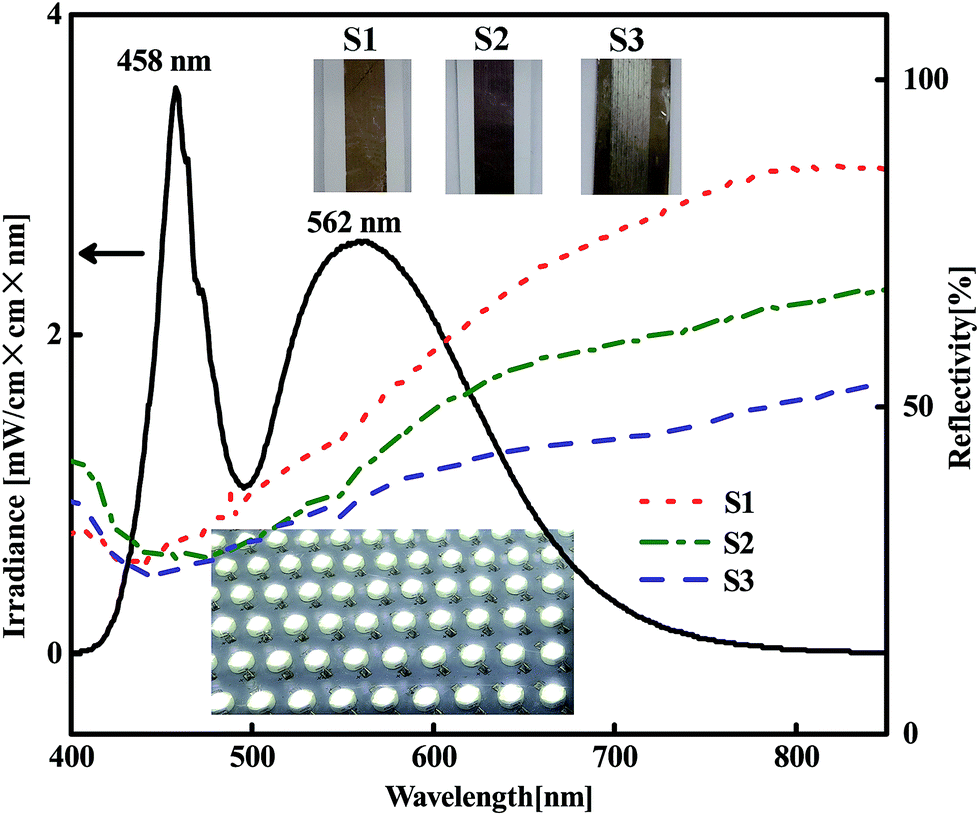 | ||
| Fig. 5 Irradiance spectra of white light LED and reflectivity spectra of the printed tracks. S1 to S3 represent the reflectivity spectra of the as-prepared silver track, the ones treated by Step 1 of MRTP and by Step 2 of MRTP, respectively. The photographs in the insets show the silver tracks of S1 to S3, and the LED light source. | ||
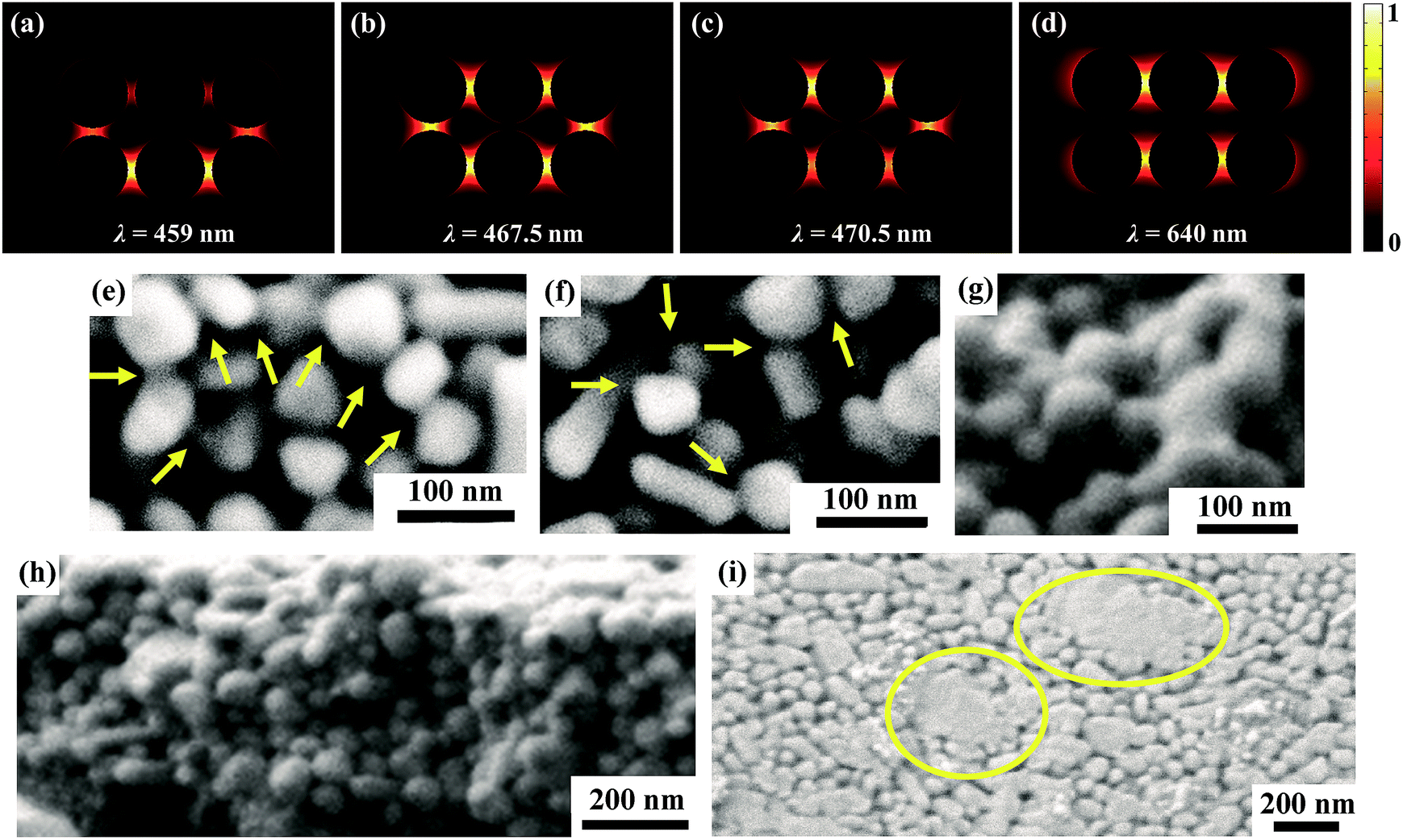 | ||
| Fig. 6 (a–d) Simulation results of electronic field distribution of silver nanoparticle aggregations at different illumination wavelengths. (e–g) High resolution SEM images of silver tracks after the treatment of Step 1 of MRTP. Arrows highlight the joining of adjacent nanoparticles. (h) and (i) SEM images show the lateral profile and front side of the silver tracks. Circles highlight the obvious morphology changes of melted silver nanoparticles at local areas. | ||
Our previous work demonstrated that when the adjacent silver nanoparticles are separated, the LSPR peak is mainly at short wavelength range, near the LSPR peak of single ones. Once the particles are linked together thoroughly, the LSPR peak red shifts to the long wavelength range obviously.40 Following this principle we measured the reflectivity spectra of three silver tracks including the as-prepared track and the ones treated by different steps of MRTP (Fig. 5). It is a direct evidence to reflect the macroscopic joining effect of the nanoparticles in the tracks. For the as-prepared track S1, there is an absorption band at about 430 nm corresponding to the LSPR band of a single silver nanoparticle.40 It indicates that most of the particles are separated in the tracks. The track S2 is treated by acetone assisted photonic sintering. It can be seen from the reflectivity spectrum that the main absorption band red shifted obviously. Meantime, the reflectivity at long wavelength range decreased obviously. It indicated that the adjacent particles have been joined together and therefore established the validity of the post-processing.
Fig. 6e–i show the SEM images of the silver tracks treated by the acetone assisted photonic sintering taken from different section views. It is clearly observed that most of the particles linked together. Seen from the lateral section view of the silver track (Fig. 6h), particles inside the silver track are densely packed and sintered together. The areas of agglomerations are easily observed in Fig. 6i. It shows clearly that some particles completely lost their original morphology and melted into bulk silver after the treatment of Step 1 of MRTP.
The electrical resistivity ρ of the printed tracks at different steps were measured by a two-probe method and calculated using a formula: ρ = R × W × H/L, when R, W, H and L represent the resistance, width, height and length of the tracks, respectively.44 A typical resistivity value after the acetone assisted photonic sintering is 1.2 × 10⁻⁷ Ω m (shown in Fig. 4a), corresponding to a conductivity up to 13.4% of that of bulk silver. To exhibit the high efficiency of the proposed acetone assisted photonic sintering process, we also investigated the conductivities of silver tracks treated either by photonic sintering or acetone immersion, seperately. After 3 hours irradiation of LED without acetone immersion, the conductivity of silver tracks increased to 1.7% of that of bulk silver. Similarly, the final conductivity of silver tracks increased to 1.05% of that of bulk silver after the tracks were immersed in acetone for a long time without the LED irradiation. These two values are much lower than the result obtained from the acetone assisted photonic sintering process above.
The second step is electroless deposition of printed tracks. Because of the intrinsic nanostructure aggregation property, even for the well sintered silver tracks, there are still many voids and defects on the surface and inside the tracks treated by Step 1 of MRTP. Here we showed that the conductivity of the tracks after the sintering process can be further improved by using the concept of material increasing manufacturing.
Electroless deposition is a chemical method to provide silver atoms and small clusters in solution.45,46 The silver tracks were immerged into the electroless deposition solution after sintering process as illustrated in Fig. 3a. As the organic shells surrounding the silver nanoparticles had been removed by the photon-sintering process, the silver nanoparticles became active and easily absorbed newly reduced atoms. During the electroless deposition, the reduced silver atoms grew rapidly along the surface of the particles and fill in the gaps between these particles. By carefully treatment, the compactness of the silver track was improved obviously as shown in Fig. 3d. The high resolution SEM image in the inset of Fig. 3d shows the newly formed small silver nanoparticles (∼20 nm) which effectively fill into the gaps between the large nanoparticles. Meantime, the size of the elemental nanoparticles did not increase obviously. That means the thickness of the silver track will not change obviously after the treatment of the electroless deposition process. The comparison of the reflectivity spectra of S2 and S3 shown in Fig. 5 provided a direct evidence to show the remarkable effect on the morphology improvement using the electroless deposition process. (1) The absorption in long wavelength range decreases obviously. It reflects that the amount of well linked nanoparticles increases significantly as discussed above. (2) Compared with the reflectivity spectrum of S2, the main absorption band of S3 at ∼430 nm blue-shifted obviously. It established that many small nanoparticles were absorbed onto the surface of the silver tracks. From the photograph of S3 shown in the inset of Fig. 5, we also observed a color change of the paper substrate from white to yellow. It is because the newly reduced silver clusters also penetrated into the paper substrate. However, these areas are non-conductive at all and therefore will not affect the functionality of the as-designed electronic circuits. More details exhibiting the effectiveness of the electroless deposition process using nanowire based ink is shown in the ESI, Fig. S3.†
As shown in Fig. 4a, one can see that the reflectivity of silver track decreased rapidly after two cycles of electroless deposition. The final resistivity reached 0.97 × 10⁻⁷ Ω m which corresponds to a conductivity up to 17% of that of bulk silver. We also compared the effects between the MRTP and the conventional thermal sintering process. For comparison, silver tracks printed with the same ink were heated by a hot plate to promote the sintering. Considering the poor heat tolerance of paper, the heating temperature was set to 120 °C. As shown from the curve, the conductivity of the silver track increased to 2 × 10⁻⁷ Ω m which is only ∼8% of that of bulk silver after a heating process of 160 min. The comparison experimental result directly shows the high efficiency of the MRTP method. The overall technology features of the described approach are compared in Table S1, ESI.†
Application in paper electronics
We printed various structures and patterns to investigate the potential applications of the synthesized silver inks and relative techniques for paper electronics. Fig. 7 shows the silver patterns with different line-widths printed by a commercial ink-jet printer. The SEM image in Fig. 7d shows the printed silver track is uniform in large scale. A single ink dot with a diameter of ∼50 μm is observed at the edge of the track. It indicates the most fine line-width printed using current printer and ink can reach as thin as several tens of micrometers. These results show the convenience and flexibility of the ink-jet printing technique.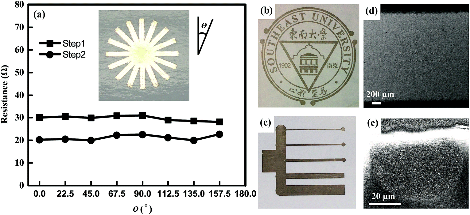 | ||
| Fig. 7 (a) Comparison of resistances along different directions of ink-jet printed pattern on paper. The printed pattern for the measurement is shown in the inset. The line-width of the tracks is 1 mm. (b) and (c) show the photographs of the printed silver patterns. (d) and (e) show the SEM images of a printed track and a single silver ink dot, respectively. | ||
For practical application in electronic circuits and devices, the printing uniformity and mechanical flexibility of the printed tracks are also needed to evaluate. We designed and printed a silver pattern containing eight intersected silver tracks with an equal cross-angle (shown in the inset of Fig. 7a). The resistances between the two terminals of each track treated after Step 1 and Step 2 of MRTP were recorded in Fig. 7a, respectively. The maximum value of the resistance differences among eight directions is less than 4% for Step 1 of MRTP, and 6.8% for Step 2 of MRTP. It indicates the uniformity of the printed tracks along different directions is excellent.
To investigate the mechanical flexibility of the silver tracks when they are bended and folded, we measured the resistance change of the tracks under different bending radius. A mold with various bending radius served as an assistant tool to control the bending of the silver track. The insets in Fig. 8 show the details of the measurement. We folded the track to a certain curvature assisted by inserting it into different channels of the mold, recorded the resistance, and then unfolded the track. This process was repeated several times, and the resistance of each time was recorded in Fig. 8 to evaluate the reliability of the silver tracks for flexible electronics application. The curvature k = 1/r, where r represents the bending radius of the track. As recorded in Fig. 8, when the curvature was set to a small value, the resistance values recorded from the repeated measurements were stable with small fluctuations. As shown in Fig. 8, the average value of the resistance increased gradually with the increase of the curvature. Meantime, the multiple measured values were still stable and fluctuated in a small range. Even when the curvature is as large as 167 m−1 (corresponding to r = 6 mm), the fluctuation of the resistance is still in the range of 2.5%. To further verify the reliability of the tracks for flexible applications, we monitored the resistance change when the track were bended to a certain curvature (r = 0.06 m) assisted by the mold for 200 times. The recorded fluctuation of the resistance is within an acceptable level. Compared with its initial value, the resistance of the silver track only increased ∼2.89% after 200 times bending test. It exhibited the possibility of realizing various 3D architecture electronic devices with stable performance using the ink-jet printed technique on papers. Moreover, it can be easily found that the strain sensitive of resistance of the silver tracks is excellent. It meets the technique requirement of high performance resistive strain sensors well.47 However, we also observed when the curvature continued to increase from 500 m−1 to 4000 m−1 (corresponding to r = 2 mm and 0.25 mm, respectively), both the values of the resistance and their fluctuation range increased obviously corresponding to a serious electrical performance deterioration. It means the current printed silver tracks are not suitable to be frequently folded in-half when they are applied to the fabrication of electronic devices requiring high stability and accuracy. The reasons why the conductivity of silver tracks is affected by the substrate bending can be explained as follows. Unlike conductive tracks constituted by bulk silver, the printed silver tracks are mainly constituted by densely compacted nanoparticles. Although these particles are joined together after post processing treatment, the mechanical strength of such tracks is still weaker compared with bulk silver, as discussed before.19,25,29 Fortunately, as indicated by our experimental result, this resistance change is recoverable when the bending curvature is small. This gradual increase of resistance in according with the change of bending curvature and recoverable property make such printed tracks useful in sensing application. However, once the curvature is too large, unrecoverable cracks and breaks inside the tracks, as well as the deformation of paper substrate will result in a serious and unrecoverable increasement of resistance. We believe such bending stability can be further improved by increasing the thickness of the tracks or optimizing the ratio between the silver nanospheres and the nanowires in the ink as discussed above and investigated by the literatures.9,37,38
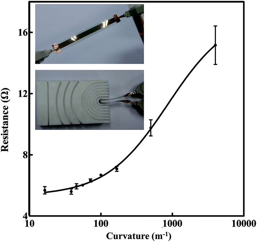 | ||
| Fig. 8 Resistance of the silver tracks as a function of the bending curvature. All the data for each experimental condition were collected for several-times repetitions. The average values and standard deviation (error bar) were labeled. Photographs of the bending track sample and the measurement details are shown in the insets. | ||
Finally, we exhibit that by combining with the 3D paper folding and color printing technologies, the paper based ink-jet printing technique can be used to realize imaginative 3D flexible electronic devices with complicated architectures and colored profiles which are difficult to fabricate by conventional techniques. We designed various 3D electronic devices dressed with colored profiles containing LEDs and printed silver tracks (Fig. 9) to introduce this concept. Three unique advantages of this technology are observed. (1) The flexibility of the paper based electronic devices is evident. Silver tracks can be bent, curled and folded easily when the devices are working.
 | ||
| Fig. 9 Photographs of various 3D colored architectures containing LEDs and printed silver tracks. | ||
(2) Silver inks and conventional color inks can be used together by ink-jet printing conveniently. The silver tracks can serve not only as electronic pathway, but also decorative lines with unique light reflection. (3) As a low-cost and easy processing raw material, the paper substrates can also be painted, bent, folded and cut into complicated sculptures and architectures easily. Such distinguishing technological advantages make the paper based ink-jet printing a highly desirable technology for future innovative electronic product fabrication. In the experiment, we found that the photo paper being used here is a type of paper very suitable for realizing such 3D paper based electronic circuits and devices. Firstly, as studied in literature48 as well as in our experiment, it is found the silver tracks printed on this type of paper has a better conductivity, mainly owing to its smooth surface. Meantime, the hardness and the machinability of such type of paper are both excellent, suitable for constructing complicated 3D architectures.
Conclusions
In this paper, we present a systematical study on paper based ink-jet printing technology from the aspects of the massive nanoparticle synthesis, high efficiency post-processing and innovative application on paper electronics. (1) We proposed a seeds triggered synthesis strategy which is robustly repeatable for the fabrication of massive silver nanoparticles. H2O2 was found a key point for the successfully etching of the initial seeds of which the amount and crystal type are difficult to control. With the seeds triggering strategy, since the chemical purity and reaction condition dependence of the synthesis is decreased significantly, massive silver nanoparticles with uniform size were achieved in a facial and repeatable method. (2) We explored the possibility of room-temperature post-processing of the printed silver tracks by incorporating different techniques. With a serial of comparison experiments and theoretical simulations, we exhibited the important role of acetone to trigger the room-temperature sintering and established the high efficiency of photonic sintering using white light LEDs. After the sintering process, electroless deposition was proved an effective method to further improve the conductivity of the tracks by the condensing of the tracks having defects and voids. The MRTP method is superior because the conductivity of the silver tracks treated by current method is two-fold higher than that of the samples treated by conventional thermal sintering at 120 °C. (3) Finally, the electrical performance investigation on the uniformity and the mechanical flexibility shows numerous advantages of the paper based ink-jet printing technology. Such flexible, paintable and tailorable paper electric circuits and devices open the possibility to realize innovative electronic products in future, and have great potential applications in sensing, display and disposable electronic chips.Acknowledgements
This work is supported by NSFC under grant numbers 61307066 and 61450110442, Natural Science Foundation of Jiangsu Province under grant number BK20130630, Doctoral Fund of Ministry of Education of China under grant number 20130092120024, the Fundamental Research Funds for the Central Universities and Graduate Innovation Program of Jiangsu Province under grant number KYLX_0126, Innovation Fund of School of Electronic Science and Engineering, Southeast University under grant number 2242015KD006.Notes and references
- M. Singh, H. M. Haverinen, P. Dhagat and G. E. Jabbour, Inkjet Printing—Process and its Applications, Adv. Mater., 2010, 22, 673–685 CrossRef CAS PubMed.
- Z. P. Yin, Y. A. Huang, N. B. Bu, X. M. Wang and Y. L. Xiong, Inkjet Printing for Flexible Electronics: Materials, Processes and Equipments, Chin. Sci. Bull., 2010, 55, 3383–3407 CrossRef.
- A. K. Yetisen, H. Qu, A. Manbachi, H. Butt, M. R. Dokmeci, J. P. Hinestroza, M. Skorobogatiy, A. Khademhosseini and S. H. Yun, Nanotechnology in Textiles, ACS Nano, 2016, 10, 3042–3068 CrossRef CAS PubMed.
- O. Mhibik, S. Chénais, S. Forget, C. Defranoux and S. Sanaur, Inkjet-printed Vertically Emitting Solid-state Organic Lasers, J. Appl. Phys., 2016, 119, 173101 CrossRef.
- P. Andersson, R. Forchheimer, P. Tehrani and M. Berggren, Printable All-organic Electrochromic Active-matrix Displays, Adv. Funct. Mater., 2007, 17, 3074–3082 CrossRef CAS.
- Y. Galagan, E. W. Coenen, R. Abbel, T. J. van Lammeren, S. Sabik, M. Barink, E. R. Meinders, R. Andriessen and P. W. M. Blom, Photonic Sintering of Inkjet Printed Current Collecting Grids for Organic Solar Cell Applications, Org. Electron., 2013, 14, 38–46 CrossRef CAS.
- G. W. Huang, H. M. Xiao and S. Y. Fu, Paper-based Silver-nanowire Electronic Circuits with Outstanding Electrical Conductivity and Extreme Bending Stability, Nanoscale, 2014, 6, 8495–8502 RSC.
- H. L. Zhu, Z. Q. Fang, C. Preston, Y. U. Li and L. B. Hu, Transparent Paper: Fabrications, Properties, and Device Applications, Energy Environ. Sci., 2014, 7, 269–287 CAS.
- R. Z. Li, A. M. Hu, T. Zhang and K. D. Oakes, Direct Writing on Paper of Foldable Capacitive Touch Pads with Silver Nanowire Inks, ACS Appl. Mater. Interfaces, 2014, 6, 21721–21729 CAS.
- M. C. Barr, J. A. Rowehl, R. R. Lunt, J. J. Xu, A. Wang, C. M. Boyce, S. G. Im, V. Bulović and K. K. Gleason, Direct Monolithic Integration of Organic Photovoltaic Circuits on Unmodified Paper, Adv. Mater., 2011, 23, 3500–3505 CrossRef CAS PubMed.
- R. Z. Li, R. Peng, K. D. Kihm, S. Bai, D. Bridges, U. Tumuluri, Z. Wu, T. Zhang, G. Compagnini, Z. Feng and A. Hu, High-rate In-plane Micro-supercapacitors Scribed onto Photo Paper Using in situ Femtolaser-reduced Graphene Oxide/Au Nanoparticle Microelectrodes, Energy Environ. Sci., 2016, 9, 1458–1467 CAS.
- L. Polavarapu, A. L. Porta, S. M. Novikov, M. Coronado-Puchau and L. M. Liz-Marzán, Pen-on-paper Approach Toward the Design of Universal Surface Enhanced Raman Scattering Substrates, Small, 2014, 10, 3065–3071 CrossRef CAS PubMed.
- Y. Aleeva and B. Pignataro, Recent Advances in Upscalable Wet Methods and Ink Formulations for Printed Electronics, J. Mater. Chem. C, 2014, 2, 6436–6453 RSC.
- S. Hong, J. Yeo, G. Kim, D. Kim, H. Lee, J. Kwon, H. Lee, P. Lee and S. H. Ko, Nonvacuum, Maskless Fabrication of a Flexible Metal Grid Transparent Conductor by Low-temperature Selective Laser Sintering of Nanoparticle Ink, ACS Nano, 2013, 7, 5024–5031 CrossRef CAS PubMed.
- S. P. Chen, J. R. D. Retamal, D. H. Lien, J. H. He and Y. C. Liao, Inkjet-printed Transparent Nanowire Thin Film Features for UV Photodetectors, RSC Adv., 2015, 5, 70707–70712 RSC.
- K. J. Lee, B. H. Jun, T. H. Kim and J. Joung, Direct Synthesis and Inkjetting of Silver Nanocrystals toward Printed Electronics, Nanotechnology, 2006, 17, 2424 CrossRef CAS.
- L. Liu, X. X. Wan, L. L. Sun, S. L. Yang, Z. G. Dai, Q. Y. Tian, M. Lei, X. H. Xiao, C. Z. Jiang and W. Wu, Anion-mediated Synthesis of Monodisperse Silver Nanoparticles Useful for Screen Printing of High-conductivity Patterns on Flexible Substrates for Printed Electronics, RSC Adv., 2015, 5, 9783–9791 RSC.
- W. F. Shen, X. P. Zhang, Q. J. Huang, Q. S. Xu and W. J. Song, Preparation of Solid Silver Nanoparticles for Inkjet Printed Flexible Electronics with High Conductivity, Nanoscale, 2014, 6, 1622–1628 RSC.
- Q. J. Huang, W. F. Shen, Q. S. Xu, R. Q. Tan and W. J. Song, Properties of Polyacrylic Acid-coated Silver Nanoparticle Ink for Inkjet Printing Conductive Tracks on Paper with High Conductivity, Mater. Chem. Phys., 2014, 147, 550–556 CrossRef CAS.
- M. Vaseem, K. M. Lee, A. R. Hong and Y. B. Hahn, Inkjet printed fractal-connected electrodes with silver nanoparticle ink, ACS Appl. Mater. Interfaces, 2012, 4, 3300–3307 CAS.
- Y. Sun, Controlled Synthesis of Colloidal Silver Nanoparticles in Organic Solutions: Empirical Rules for Nucleation Engineering, Chem. Soc. Rev., 2013, 42, 2497–2511 RSC.
- B. Wiley, T. Herricks, Y. G. Sun and Y. N. Xia, Polyol Synthesis of Silver Nanoparticles: Use of Chloride and Oxygen to Promote the Formation of Single-crystal, Truncated Cubes and Tetrahedrons, Nano Lett., 2004, 4, 1733–1739 CrossRef CAS.
- S. Wünscher, R. Abbel, J. Perelaer and U. S. Schubert, Progress of Alternative Sintering Approaches of Inkjet-printed Metal Inks and their Application for Manufacturing of Flexible Electronic Devices, J. Mater. Chem. C, 2014, 2, 10232–10261 RSC.
- T. Y. Dong, W. T. Chen, C. W. Wang, C. P. Chen, C. N. Chen, M. C. Lin, J. M. Song, I. G. Chen and T. H. Kao, One-step Synthesis of Uniform Silver Nanoparticles Capped by Saturated Decanoate: Direct Spray Printing Ink to Form Metallic Silver Films, Phys. Chem. Chem. Phys., 2009, 11, 6269–6275 RSC.
- P. Peng, A. M. Hu, A. P. Gerlich, G. Zou, L. Liu and Y. N. Zhou, Joining of Silver Nanomaterials at Low Temperatures: Processes, Properties, and Applications, ACS Appl. Mater. Interfaces, 2015, 7, 12597–12618 CAS.
- Y. Ma, H. Li, D. Bridges, P. Peng, B. J. Lawrie, Z. L. Feng and A. M. Hu, Zero-dimensional to Three-dimensional Nanojoining: Current Status and Potential Application, RSC Adv., 2016, 6, 75916–75936 RSC.
- A. Hu, J. Y. Guo, H. Alarifi, G. Patane, Y. Zhou, G. Compagnini and C. X. Xu, Low Temperature Sintering of Ag Nanoparticles for Flexible Electronics Packaging, Appl. Phys. Lett., 2010, 97, 153117 CrossRef.
- P. Peng, A. M. Hu, A. P. Gerlich, Y. Liu and Y. N. Zhou, Self-generated Local Heating Induced Nanojoining for Room Temperature Pressureless Flexible Electronic Packaging, Sci. Rep., 2015, 5, 9282 CrossRef CAS PubMed.
- R. Z. Li, A. M. Hu, D. Bridges, T. Zhang, K. D. Oakes, R. Peng, U. Tumuluri, Z. L. Wu and Z. L. Feng, Robust Ag Nanoplate Ink for Flexible Electronics Packaging, Nanoscale, 2015, 7, 7368–7377 RSC.
- M. Grouchko, A. Kamyshny, C. F. Mihailescu, D. F. Anghel and S. Magdassi, Conductive Inks with a “Built-in” Mechanism that Enables Sintering at Room Temperature, ACS Nano, 2011, 5, 3354–3359 CrossRef CAS PubMed.
- S. Magdassi, M. Grouchko, O. Berezin and A. Kamyshny, Triggering the Sintering of Silver Nanoparticles at Room Temperature, ACS Nano, 2010, 4, 1943–1948 CrossRef CAS PubMed.
- M. Y. Lee, J. Y. Lee, W. J. Lee, S. Y. Kim, Y. H. Park, T. Mosaiab, S. Y. Park and I. In, Photocatalytic Effect of TiO2 Nanoparticles on Room-temperature Sinterable Silver Nanoparticle Ink with Poly(N-vinylpyrrolidone) Ligand, Chem. Lett., 2013, 42, 649–650 CrossRef CAS.
- L. Y. Xu, G. Y. Yang, H. Y. Jing, J. Wei and Y. D. Han, Pressure-assisted Low-temperature Sintering for Paper-based Writing Electronics, Nanotechnology, 2013, 24, 355204 CrossRef CAS PubMed.
- H. Yuan, C. G. Khoury, H. Hwang, C. M. Wilson, G. A. Grant and T. Vo-Dinh, Gold Nanostars Surfactant-free Synthesis, 3D Modelling, and Two-photon Photoluminescence Imaging, Nanotechnology, 2012, 23, 075102 CrossRef PubMed.
- T. Zhang, Y. J. Song, X. Y. Zhang and J. Y. Wu, Synthesis of Silver Nanostructures by Multistep Methods, Sensors, 2014, 14, 5860–5889 CrossRef PubMed.
- Y. T. Yen, T. Y. Lu, Y. C. Lee, C. C. Yu, Y. C. Tsai, Y. C. Tseng and H. L. Chen, Highly Reflective Liquid Mirrors: Exploring the Effects of Localized Surface Plasmon Resonance and the Arrangement of Nanoparticles on Metal Liquid-like Films, ACS Appl. Mater. Interfaces, 2014, 6, 4292–4300 CAS.
- J. T. Wu, S. L. C. Hsu, M. H. Tsai, Y. F. Liu and W. S. Hwang, Direct Ink-jet Printing of Silver Nitrate–Silver Nanowire Hybrid Inks to Fabricate Silver Conductive Lines, J. Mater. Chem., 2012, 22, 15599–15605 RSC.
- P. Peng, A. Hu, B. Zhao, A. P. Gerlich and Y. N. Zhou, Reinforcement of Ag Nanoparticle Paste with Nanowires for Low Temperature Pressureless Bonding, J. Mater. Sci., 2012, 47, 6801–6811 CrossRef CAS.
- G. C. Messina, M. G. Sinatra, V. Bonanni, R. Brescia, A. Alabastri, F. Pineider, G. Campo, C. Sangregorio, G. Li-Destri, G. Sfuncia, G. Marletta, M. Condorelli, R. P. Zaccaria, F. De Angelis and G. Compagnini, Tuning the Composition of Alloy Nanoparticles Through Laser Mixing: The Role of Surface Plasmon Resonance, J. Phys. Chem. C, 2016, 120, 12810–12818 CAS.
- T. Zhang, X. Y. Zhang, X. J. Xue, X. F. Wu, C. Li and A. Hu, Plasmonic Properties of Welded Metal Nanoparticles, Open Surf. Sci. J., 2011, 3, 76–81 CrossRef CAS.
- F. Pincella, Y. J. Song, T. Ochiai, K. Isozaki, K. Sakamoto and K. Miki, Square-centimeter-scale 2D-arrays of Au@Ag Core–Shell Nanoparticles towards Practical SERS Substrates with Enhancement Factor of 107, Chem. Phys. Lett., 2014, 605, 115–120 CrossRef.
- X. Y. Zhang, A. M. Hu, T. Zhang, W. Lei, X. J. Xue, Y. H. Zhou and W. W. Duley, Self-assembly of Large-scale and Ultrathin Silver Nanoplate Films with Tunable Plasmon Resonance Properties, ACS Nano, 2011, 5, 9082–9092 CrossRef CAS PubMed.
- X. Y. Zhang, T. Zhang, A. Hu, Y. J. Song and W. W. Duley, Controllable Plasmonic Antennas with Ultra Narrow Bandwidth Based on Silver Nano-flags, Appl. Phys. Lett., 2012, 101, 153118 CrossRef.
- L. Y. Xu, G. Y. Yang, H. Y. Jing, J. Wei and Y. D. Han, Ag–Graphene Hybrid Conductive Ink for Writing Electronics, Nanotechnology, 2014, 25, 055201 CrossRef CAS PubMed.
- P. N. Vinod, The Electrical and Microstructural Properties of Electroplated Screen-printed Ag Metal Contacts in Crystalline Silicon Solar Cells, RSC Adv., 2013, 3, 14106–14113 RSC.
- N. F. Fahim, B. Jia, Z. Shi and M. Gu, Simultaneous Broadband Light Trapping and Fill Factor Enhancement in Crystalline Silicon Solar Cells Induced by Ag Nanoparticles and Nanoshells, Opt. Express, 2012, 20, A694–A705 CrossRef CAS PubMed.
- M. Bona, E. Sardini, M. Serpelloni and C. O. Lombardo, Study on a Telemetrie System that Works with an Inkjet-printed Resistive Strain Gauge, IEEE Sensors Applications Symposium, 2016, 1–6 Search PubMed.
- K. Dogome, T. Enomae and A. Isogai, Method for Controlling Surface Energies of Paper Substrates to Create Paper-based Printed Electronics, Chem. Eng. Process., 2013, 68, 21–25 CrossRef CAS.
Footnote |
| † Electronic supplementary information (ESI) available: This section includes the investigation of the relationship between the thickness of the tracks and the printing cycles, SEM image and absorbance spectrum of gold seeds, comparison experiment for the investigation of organic shell dissolving ability of different organic solvents, the simulation modeling of the electromagnetic field distribution analysis, comparison of particle synthesis and post processing methods, and post-processing of silver tracks formed by large silver crystal structures using electroless silver deposition. See DOI: 10.1039/c6ra27163d |
| This journal is © The Royal Society of Chemistry 2017 |