DOI:
10.1039/C6RA26984B
(Paper)
RSC Adv., 2017,
7, 9596-9604
The photovoltaic effect in a [001] orientated ZnO thin film and its physical mechanism†
Received
18th November 2016
, Accepted 24th January 2017
First published on 1st February 2017
Abstract
We report a new type of photovoltaic effect. The photovoltaic device was constructed using a [001] orientated wurtzite ZnO thin film synthesized by heating Zn(NO3)2 solution. The open-circuit voltage (Voc) and short-circuit current (Isc) of the ZnO photovoltaic device are 0.16 mV and 0.25 μA, respectively, under 365 nm ultraviolet lamp (3 W) illumination. Current rectification across the top and bottom planes of the ZnO thin film was observed. The photovoltaic and rectifying properties of the ZnO thin film are related to the magnitude of the TC(002). An internal electric field is produced in the ZnO film by spontaneous polarization in the [001] direction. The presence of the internal electric field is the fundamental physical basis of the photovoltaic effect, and a new physical mechanism of photon-to-electron conversion is proposed. The electrostatic potential provides a driving force for flow of the photogenerated electrons and holes in the semiconductor and in an external load, and thus the photo-to-electron conversion is achieved. Our result suggests thin film texturing as a strategy to develop photovoltaic devices beyond p–n junction. In addition, the photo-to-electron conversion model provides new insights into the understanding of the photovoltaic effect in ferroelectric and pyroelectric materials as well as the design and fabrication of advanced solar cells and other electronic and optoelectronic devices.
1. Introduction
Solar energy represents the most abundant and yet one of the least harvested sources of renewable energy.1 Photovoltaic solar cells are the most common form of light to electrical power converters. Since the discovery of silicon-based solar cells,2 a few types of solar cell, such as semiconductor cells with p–n junctions,3–8 polymer–inorganic hybrid cells9–13 and dye-sensitized solar cells14–20 have been developed. Recently, solar cells based on coaxial silicon nanowires with p–n and p–i–n radial heterostructures have been fabricated.3–5 Nanoparticles, nanorods and nanowires have been used to improve charge collection efficiency in polymer-blend11 and dye-sensitized solar cells,15,20 to demonstrate carrier multiplication,21 and to enable low-temperature processing of photovoltaic devices.20,22 However, the charge separation principle of photogenerated electrons and holes in the solar cells has stayed the same without significant advance.
Moreover, photovoltaic effect has been observed in many ferroelectric and pyroelectric materials, such as BaTiO3,23,24 BiFeO3,25–28 Pb(Zr,Ti)O3,29–31 Bi2FeCrO6 32 and ZnS.33 The photovoltaic effect in ferroelectric materials is relied on the polarization electric field, and the photovoltage was related to the magnitude of the remanent polarization.23,24 In striated ZnS crystals, the photovoltage was always in the direction of the pyroelectric axis.33 Nevertheless, the detailed mechanism involved in the photovoltaic effect is not yet known.
Recently, the numerous semiconductor nanocrystals with exposed polar facets have been found to show enhanced photocatalytic activities.34–42 Based on the ZnO {001} and NiO, CoO and Cu2Se {111} polar structures,39–43 we proposed a new concept, there is an internal electric field between positive and negative polar semiconductor planes, and described charge separation between polar semiconductor surfaces and photocatalysis mechanism in detail.39–43 On the basis of the concept of an internal electric field existing between polar semiconductor planes, we develop a new type of photovoltaic device constructed using an [001] orientated wurtzite ZnO thin film. It is free of p–n junction. The photovoltaic and rectifying properties of the ZnO film device depend on the TC(002). The presence of the internal electric field in the [001] orientated ZnO film is the fundamental physical basis of the ZnO thin film photovoltaic device, and a new physical mechanism of photon-to-electron conversion is proposed.
2. Experimental section
2.1. Sample preparation
Preparation of the [001] orientated ZnO thin film: Zn(NO3)2·6H2O used was of analytical grade. 0.5 mol L−1 of Zn(NO3)2 aqueous solution was obtained by dissolving 0.2975 g of Zn(NO3)2·6H2O in 2.0 mL de-ionized water (2.0 × 1.2 cm2). The [001] orientated ZnO thin film was prepared by heating Zn(NO3)2 solution. In a typical procedure, one of 0.5 M Zn(NO3)2 aqueous solution was added on a fluorine-doped tin oxide (FTO) glass substrate. The FTO glass substrate was placed in a quartz boat. The quartz boat was placed at center of a tubular electric furnace at 450 °C. After 10 min, the boat was taken out and cooled to room temperature. A white thin film was grown on the FTO substrate.
2.2. Characterization
The as-prepared thin films were characterized using X-ray diffraction (XRD), scanning electron microscopy (SEM) and transmission electron microscopy (TEM). The XRD patterns was recorded with a Haoyuan DX-2700 X-ray diffractometer operating with Cu Kα1 radiation (λ = 1.54 Å). SEM observations were carried out with a FEI Quanta 200 scanning electron microscope at an accelerating voltage of 25 kV. TEM and electron diffraction images were obtained on a JEOL JEM-3010 TEM at an accelerating voltage of 300 kV. Electrical properties of ZnO thin films with (001) preferred orientation were recorded by a Keithley 2601 source measurement unit at room temperature.
3. Results and discussion
3.1. Synthesis and characterization of the ZnO thin film
The ZnO thin film with (001) preferred orientation was fabricated by heating Zn(NO3)2 solutions on a FTO glass substrate at 450 °C. The SEM images in Fig. 1a–c reveal that surface of the thin film is very rough, there is a large quantity of pits with the sizes of 4.0 to 9.5 μm on the surface. Thickness and area of the film is about 4.0 μm, and 0.6 cm2, respectively. The XRD measurements (Fig. 1d) show that the as-synthesized rough thin film is wurtzite ZnO with a hexagonal structure. The (002) diffraction peak is overwhelming, and other peaks are very weak, revealing a strong [001] preferred orientation. The texture coefficient of (002) plane was calculated from the following equation:44
where I(hkl) are measured intensities of (hkl) reflection, I0(hkl) are powder diffraction intensities of wurtzite ZnO according to the Joint Committee on Powder Diffraction Standards card no. 36-1451, and n is the number of diffraction peaks used in the calculations. For powders with random crystallographic orientations, the texture coefficient is 1. The TC of (002) for the as-obtained ZnO film is 4.07, indicating that the film is enclosed by (001) top and (00![[1 with combining macron]](https://www.rsc.org/images/entities/char_0031_0304.gif) ) bottom surfaces. Fig. 2a presents a representative TEM image of the ZnO film with a size of about 5.8 μm. Fig. 2b–e show selected area electron diffraction (SAED) patterns and high-resolution TEM (HRTEM) images from the box 1 and 2 in 2a, respectively. The SAED patterns shown in Fig. 2b and d can be indexed to [001] zone axis of single-crystalline ZnO with the hexagonal structure, respectively. The lattice spacing of 0.28 nm between adjacent lattice planes (Fig. 2c and e) corresponds to the distance between two (100) facets. The SAED and HRTEM results further confirm that the ZnO film is single crystalline and enclosed by ±(001) top and bottom surfaces. The schematic illustration of crystal orientation of the ZnO thin film is shown in Fig. 2f.
) bottom surfaces. Fig. 2a presents a representative TEM image of the ZnO film with a size of about 5.8 μm. Fig. 2b–e show selected area electron diffraction (SAED) patterns and high-resolution TEM (HRTEM) images from the box 1 and 2 in 2a, respectively. The SAED patterns shown in Fig. 2b and d can be indexed to [001] zone axis of single-crystalline ZnO with the hexagonal structure, respectively. The lattice spacing of 0.28 nm between adjacent lattice planes (Fig. 2c and e) corresponds to the distance between two (100) facets. The SAED and HRTEM results further confirm that the ZnO film is single crystalline and enclosed by ±(001) top and bottom surfaces. The schematic illustration of crystal orientation of the ZnO thin film is shown in Fig. 2f.
 |
| | Fig. 1 (a–c) SEM images and (d) XRD pattern of the as-synthesized ZnO thin film. The stick pattern is the standard XRD pattern of wurtzite ZnO powders with Cu Kα1 radiation (Joint Committee on Powder Diffraction Standards Card no. 36-1451). | |
 |
| | Fig. 2 (a) A representative TEM image of the ZnO thin film with a size of about 6.0 μm. (b and c) and (d and e) SAED pattern and HRTEM image from the box 1 and 2 in (a), respectively. (f) The schematic illustration of crystal orientation of the ZnO thin film. | |
3.2. Photovoltaic device based on the ZnO thin film
A photovoltaic device was constructed using the [001] orientated ZnO thin film, and its schematic diagram is shown in Fig. 3a. The contact between the FTO glass electrode and the top surface of ZnO thin film is achieved by using a clamp. The photovoltaic properties of the ZnO thin film were characterized under a 365 nm ultraviolet (UV) lamp (3 W) illumination. The illumination area is about 2 cm2, and the distance between the lamp and ZnO thin film is approximately 2 cm. Current–voltage (I–V) curves measured at a bias of 0.6 mV are shown in Fig. 3b. The I–V data recorded from the device yields an open-circuit voltage (Voc) of about 0.16 mV, a short-circuit current (Isc) of 0.25 μA. The value of fill factor is 20.0%. The results reveal that a photovoltaic device can be constructed using an [001] orientated wurtzite ZnO thin film. In the photovoltaic device, when the both FTO electrodes are all located on the top (001) surface of the ZnO thin film (Fig. 3c), the as-obtained dark and light I–V curves are presented in Fig. 3d. We notice that the UV-exposed ZnO thin film merely has a lower resistivity, and does not exhibit a photovoltaic property. The results reveal that the photovoltaic property rests with the orientation of the ZnO thin film. None but when the two electrodes are attached to top and bottom surfaces of the ZnO thin film, respectively, the ZnO thin film shows photovoltaic behavior. Moreover, when the UV lamp was turned on and off, the Voc and Isc were measured without power supply. The schematic diagram of the current-sensing measurement is shown in Fig. 4a. Fig. 4b and c plots the Voc and Isc as a function of time as the UV-lamp was switched on and off, respectively. It is evident that the Voc and Isc can be reversibly changed between 0 and 0.16 mV and between 0 and 0.25 μA, respectively. I–V measurements were studied under the different UV light intensities, and the different UV light intensities are achieved by changing the distance between the lamp and ZnO thin film. Fig. 5a shows I–V curves measured under illumination of the UV lamp at the distances of 1.0 to 5.0 cm. Obviously, UV light intensity reduced with an increase on the distance between the lamp and ZnO film, and thus Voc and Isc decreased. In addition, the I–V curves of the ZnO thin film were measured under a 450 nm blue light or 520 nm green light lamp illumination, and the results are shown in Fig. 5b. It was found that values of the Voc and Isc obtained under illumination of both the blue light and green light lamps are distinctly lower than that obtained under the UV lamp illumination. ZnO has a band gap 3.37 eV, (corresponding to wavelength 368 nm), the UV light can induce excitation of electrons from the top of the valence band to the bottom of the conductor band, but 450 nm blue light and 520 nm green light can not, the UV lamp is thus used. The results further indicate that the photon-to-electron conversion can be achieved by the [001] orientated ZnO thin film.
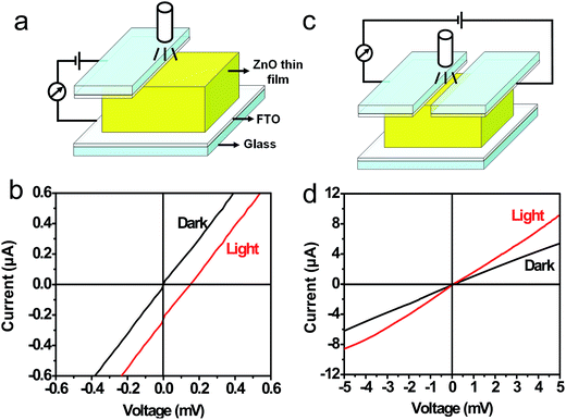 |
| | Fig. 3 (a and c) Schematic diagram of the current sensing measurement. (b and d) Current–voltage (I–V) data obtained from (a) and (c), respectively, under a 365 nm UV lamp (3 W) illumination. | |
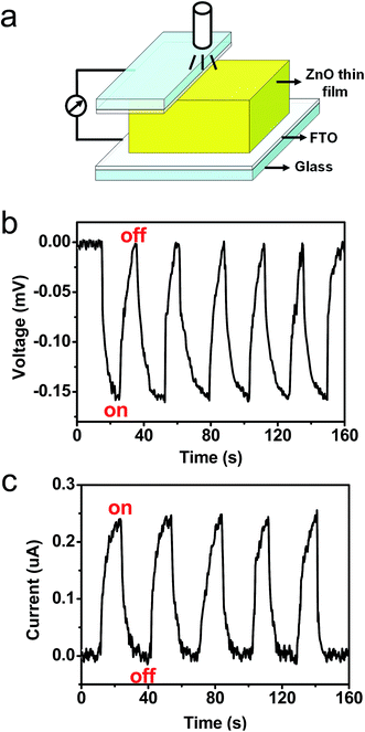 |
| | Fig. 4 (a) Schematic diagram of the solar cell. (b and c) The measured Voc and Isc when the UV lamp was turned on and off. | |
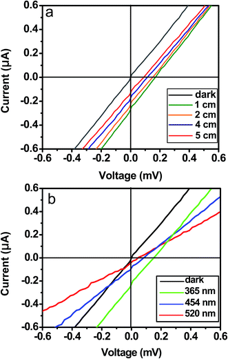 |
| | Fig. 5 (a) I–V curves measured under illumination of the UV lamp at the distances of 1.0 to 5.0 cm. (b) I–V curves of the ZnO thin film were measured under a 450 nm blue light or 520 nm green light lamp illumination. | |
3.3. An internal electric field within the ZnO thin film
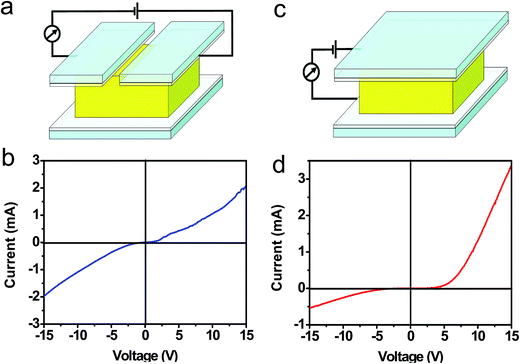
Electrical transport through the [001] orientated ZnO thin film was investigated in dark, the dark I–V curves measured at a bias of 15 V are shown in Fig. 6a–d. When the both FTO electrodes are all located on the top (001) surface of the ZnO thin film (Fig. 6a), the as-obtained I–V curve exhibit nonlinear behavior (Fig. 6b) and under a negative applied bias were symmetrically repeated under a positive applied bias, which is similar to those observed in nanocontacts between (La0.7Sr0.3)MnO3 crystals45 and between Au wires.46 The FTO–ZnO(001)–FTO contacts are not Schottky junction because that Schottky junction is a contact between a metal and a semiconductor that has rectifying properties.47 According to ref. 45, 46 and 48, the symmetrical nonlinear I–V curve is typical for tunneling barrier formation in FTO–ZnO(001)–FTO contacts. That is, the FTO–ZnO(001)–FTO contacts are defective ohmic contacts. However, when the FTO electrode is located on the top (001) and bottom (00) surfaces of the ZnO thin film, respectively (Fig. 6c), the as-obtained I–V curve exhibits a diode-like property (Fig. 6d), that is, little current flows in reverse bias, whereas there is a sharp current onset in forward bias. This diode-like behavior is similar to the p–n junction diodes,49 the basis for many critical electronic and optoelectronic devices. In a standard p–n junction, rectification arises from the potential barrier formed at the interface between p- and n-type materials.48 The results indicate that the I–V characteristic of the ZnO thin film depends on its orientation. None but as the two electrodes are attached to top and bottom surfaces of the ZnO thin film, respectively, the ZnO thin film shows rectification property.
 |
| | Fig. 6 (a and b) Schematic diagram of the current sensing measurement. (c and d) I–V curves obtained from (a) and (c), respectively. | |
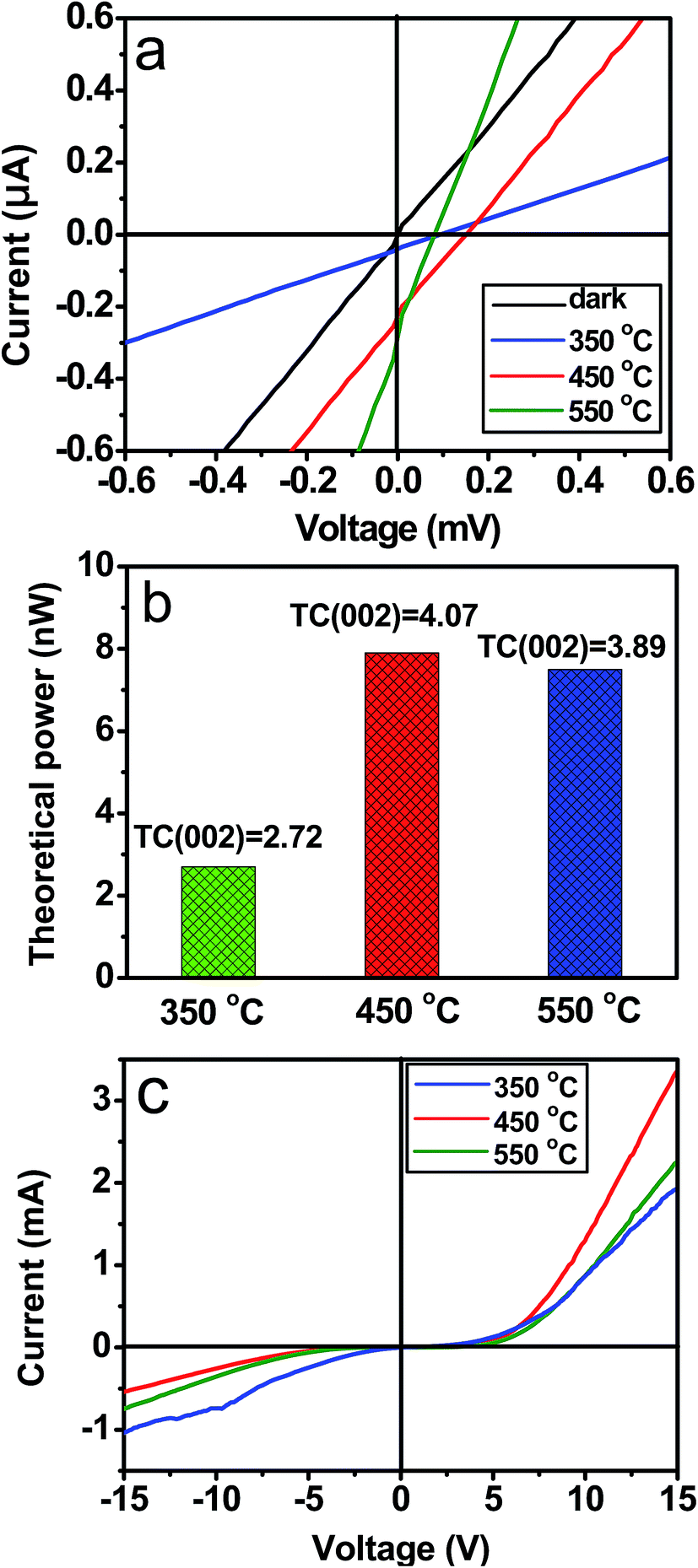
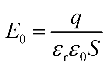
ZnO thin films with various texture coefficients of (002) can be obtained by changing the reaction temperature. SEM images and XRD patterns of the ZnO thin films synthesized by heating Zn(NO3)2 solutions at 350 and 550 °C for 10 min on the FTO glass substrates are shown in Fig. S1 and S2,† respectively. The SEM and XRD observations reveal that the products obtained at 350 and 550 °C are also the wurtzite ZnO thin films with very rough surfaces, and their thickness is about 4.0 μm. Area of the both ZnO thin films is about 0.6 cm2. Moreover, it is found that the both ZnO thin films show lower intensity ratios of (001) to other diffraction peaks in comparison with those from XRD pattern of the ZnO thin films obtained at 450 °C (Fig. 1d). Texture coefficients of (002) of the as-obtained ZnO films at 350 and 550 °C are 2.72 and 3.89, respectively, they are lower than 4.07 of the ZnO thin films obtained at 450 °C.
The photovoltaic properties of the as-obtained ZnO films at 350 and 550 °C are characterized under the 365 nm ultraviolet lamp illumination, the results are shown in Fig. 7a. Apparently, the photovoltaic effect is also observed in the both ZnO films. Under UV light irradiation, Voc of the ZnO films obtained at 350 and 550 °C is 0.10 and 0.08 mV, respectively, and their Isc is 0.05 and 0.32 μA, respectively. The TC(002), Voc, Isc and theoretical power of the ZnO films obtained at different reaction temperatures are summarized in Table 1 and Fig. 7b. To all appearances, Voc and theoretical power of the ZnO thin film devices increase with the TC(002), and thus the photovoltaic properties can be improved by increasing the TC(002). In addition, the dark I–V curves of the ZnO films obtained at 350 and 550 °C were measured at a bias of 15 V, and the results are shown in Fig. 7c. It was found that when the TC(002) of the ZnO films decreases the forward current reduces and reverse current increases. That is, the rectifying properties of the ZnO films depend on the TC(002).
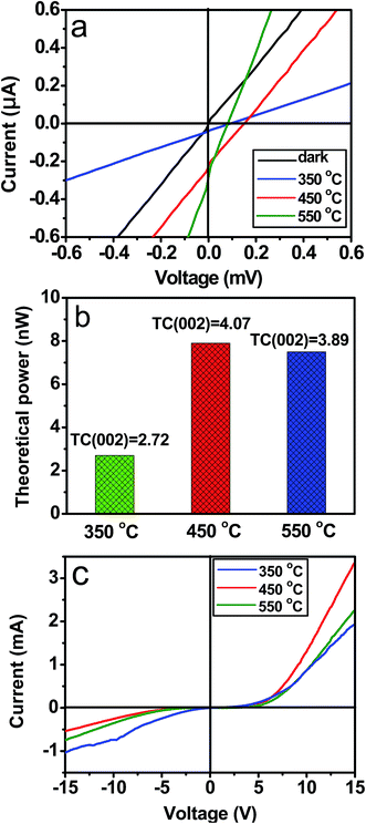 |
| | Fig. 7 (a and b) Photovoltaic properties of the ZnO thin films with various texture coefficients of (002) obtained at different temperatures under the UV lamp illumination. (c) Dark I–V curves of this three kinds of ZnO thin films along [001] direction. | |
Table 1 The TC(002) and the Voc, Isc and theoretical power of the ZnO films obtained at different reaction temperatures
| Sample No. |
Temperature (°C) |
Time (min) |
TC(002) |
Voc (mV) |
Isc (μA) |
Theoretical power (nW) |
| I |
350 |
10 |
2.72 |
0.10 |
0.05 |
0.005 |
| II |
450 |
10 |
4.07 |
0.16 |
0.25 |
0.040 |
| III |
550 |
10 |
3.89 |
0.08 |
0.32 |
0.026 |
In addition, XRD, photovoltaic property and dark I–V curves of an [001] orientated single-crystalline ZnO wafer with a thickness of 0.5 mm and a size of 1.0 × 1.0 cm2 were measured, and the results are shown in Fig. S3.† Fig. S3a† shows XRD pattern of the single-crystalline ZnO wafer. Only the (002) and (004) peaks were observed in the XRD pattern, which confirms that the single-crystalline ZnO wafer is enclosed by ±(001) top and bottom surfaces. The schematic illustration of crystal orientation of the single-crystalline ZnO wafer is shown in inset of Fig. S3a.† Fig. S3b and c† shows the photovoltaic property and dark I–V curve of the [001] orientated single-crystalline ZnO wafer, respectively. The Voc and Isc of the single-crystalline ZnO wafer are 0.27 mV and 1.08 μA, respectively. I–V curve in Fig. S3c† displays diode-like properties. The results indicate that the [001] orientated single-crystalline ZnO also exhibits photovoltaic and rectifying properties.
Moreover, the ZnO thin films with a range of (002) texture coefficients also can be synthesized by heating Zn(NO3)2 solutions at 350, 450 and 550 °C on a indium-doped tin oxide (ITO) coated glass substrate. XRD observations (Fig. 8a) reveal that TC(002) of the products can be changed by adjusting the heating temperature, TC(002) value of the as-obtained ZnO films at 350, 450 and 550 °C is 2.88, 4.16 and 3.90, respectively. Photovoltaic property and dark I–V curves of the ZnO thin films with different TC(002) were measured, and the results are shown in Fig. 8b and Table 2. Apparently, the Voc, Isc and theoretical power of the ZnO thin film devices increase with an increase on the TC(002), and the rectifying property was improved (Fig. 8c). On the basis of the investigations described above, we conclude that the rectification and photovoltaic properties are caused by the ZnO thin film with [001] preferred orientation instead of the ZnO/FTO interfaces. There is an internal electric field in the [001] orientated ZnO thin film.
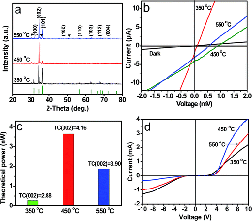 |
| | Fig. 8 (a) XRD patterns of ZnO thin films synthesized by heating Zn(NO3)2 solutions on the ITO glass substrates. (b and c) Photovoltaic properties and (d) dark I–V curves of the ZnO thin films with different texture coefficients of (002) on the ITO glass substrates. | |
Table 2 The TC(002) and the Voc, Isc and theoretical power of the ZnO films obtained at different reaction temperatures on the ITO glass substrates for 10 min
| Sample No. |
Temperature (°C) |
TC(002) |
Voc (mV) |
Isc (μA) |
Theoretical power (nW) |
| i |
350 |
2.88 |
0.12 |
2.35 |
0.28 |
| ii |
450 |
4.16 |
0.88 |
4.15 |
3.65 |
| iii |
550 |
3.90 |
0.56 |
3.36 |
1.88 |
3.4. Physical mechanism of photovoltaic effect
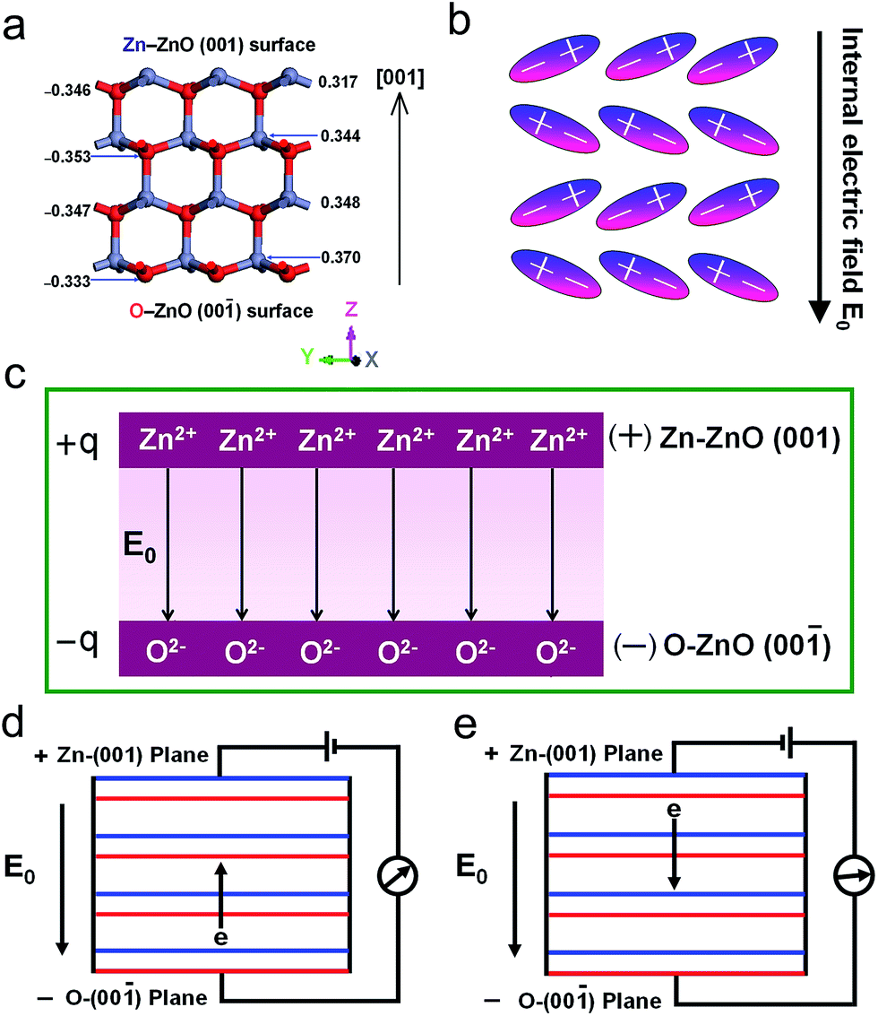
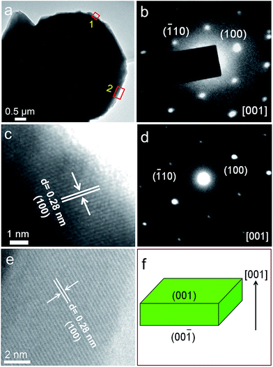
According to ref. 43, the structure and atomic charge of wurtzite ZnO in [001] direction is shown in Fig. 9a, each layer contains all positive Zn2+ ions or all negative O2− ions in the [001] direction, the positive and negative charge distribution is shown in Fig. 9b. The charge center of the cation and anion separates and result in an electric dipole. The electric dipole can create an electric field. An internal electric field E0 is therefore generated from the positive Zn–ZnO (001) to negative O–ZnO (00) planes due to the spontaneous polarization. In other word, the polar structure can be considered to a parallel-plate capacitor constructed with a positive Zn–ZnO (001) plate and a negative O–ZnO (00) plate, as shown in Fig. 9c. There is an uniform internal electric field E0 between Zn–ZnO (001) and O–ZnO (00) plates, and its magnitude is defined as follows:
where q is electric change on Zn–ZnO (001) or O–ZnO (00) plate, S is area of the plate, εr and ε0 are relative permittivity of ZnO in [001] direction and the vacuum permittivity, respectively.
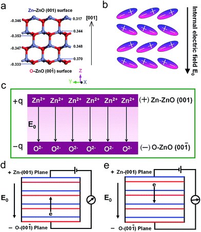 |
| | Fig. 9 (a) The structure and atomic charge of wurtzite ZnO in [001] direction. Copyright 2015, Elsevier. (b) The positive and negative charge distribution in [001] direction. (c) Schematic diagram of the parallel-plate capacitor constructed with a positive Zn–ZnO (001) plate and a negative O–ZnO (00) plate. Schematic diagram of (d) the forward-biased and (e) reverse biased [001] orientated ZnO thin film. | |
When a battery is connected across the ZnO thin film, the as-obtained dark I–V curve at a bias of 15 V exhibits a diode-like property. Under forward bias conditions, the positive terminal of the battery is attached to the positive Zn–ZnO (001) plane and the negative terminal to the negative O–ZnO (00) plane, as shown in Fig. 9d. The applied bias V is in the same direction to the internal electric field E0. The voltage V across the ZnO thin film increases. The higher voltage drive electrons and holes migrate to positive Zn–ZnO (001) planes and negative O–ZnO (00) planes, respectively, thus, there is a sharp current onset in forward bias. Under reverse bias conditions, the positive Zn–ZnO (001) plane is connected to the negative terminal and the negative O–ZnO (00) plane to the positive terminal, as depicted schematically in Fig. 9e. The applied bias is in the opposite direction to internal electric field E0, the flow of electrons and holes is prevented by the internal electric field E0 in the ZnO thin film, there therefore is a very small reverse current.
The presence of the internal electric field E0 from the Zn–ZnO (001) to O–ZnO (00) plane is the fundamental physical basis of the ZnO thin film photovoltaic device. When the [001] orientated ZnO thin films was irradiated by a 365 nm UV lamp. The electrons from the top of the valence band are excited to the bottom of the conductor band, generating electron–hole pairs in the ZnO thin film (Fig. 10a). The photogenerated electrons and holes migrate to positive polar Zn–ZnO (001) and negative polar O–ZnO (00) planes, respectively, under the internal electric field E0 (Fig. 10b). When these electrons and holes were collected by the top and bottom electrodes connected to an external load, the photon energy is converted into electricity. Photoinduced electrons and holes were separated under the internal electric field E0, creating a photovoltage, the photovoltage is in the opposite direction to internal electric field E0. The spontaneous polarization take place in the [001] direction of wurtzite ZnO, and thus the electric dipole and the internal electric field E0 increase in the ZnO thin film with the TC(002). The rectification and photovoltaic properties are therefore improved by increasing the TC(002).
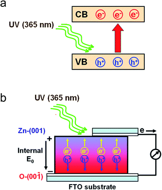 |
| | Fig. 10 (a) Generation of the photogenerated electrons and holes. (b) Flow of the photogenerated charges driven by the internal electric field. | |
4. Conclusions
An [001] orientated wurtzite ZnO photovoltaic device without p–n junction was obtained in this work. The principle of the photovoltaic effect is distinct from that of semiconductor cells with p–n junction. Based on the polar structure of ZnO {001} facets, a new physical mechanism of photo-to-electron conversion was proposed. An internal electric field is generated from the positive Zn–ZnO (001) to negative O–ZnO (00) planes due to the spontaneous polarization. The electrostatic potential provides a driving force for flow of the photogenerated electrons and holes. The present study motivates us to further develop photovoltaic devices beyond p–n junction by the thin film texturing strategy. Moreover, the photo-to-electron conversion mechanism may be applied to photovoltaic effect in ferroelectric and pyroelectric materials and provides a new insight into the design and fabrication of advanced solar cells and other electronic and optoelectronic devices.
Acknowledgements
This work was supported by the National Natural Science Foundation of China (Grant No. 21073116 and 21501116), and the Fundamental Research Funds for the Central Universities (GK 201601003).
Notes and references
- Z. Y. Fan, H. Razavi, J. W. Do, A. Moriwaki, O. Ergen, Y. L. Chueh, P. W. Leu, J. C. Ho, T. Takahashi, L. A. Reichertz, S. Neale, K. Yu, M. Wu, J. W. Ager and A. Javey, Nat. Mater., 2009, 8, 648–653 CrossRef CAS PubMed.
- D. M. Chapin, C. S. Fuller and G. L. Pearson, J. Appl. Phys., 1954, 25, 676–677 CrossRef CAS.
- B. Tian, Z. T. J. Kempa and C. M. Lieber, Chem. Soc. Rev., 2009, 38, 16–24 RSC.
- A. I. Hochbaum and P. D. Yang, Chem. Rev., 2010, 110, 527–546 CrossRef CAS PubMed.
- B. Z. Tian, X. L. Zheng, T. J. Kempa, Y. Fang, N. F. Yu, G. H. Yu, J. L. Huang and C. M. Lieber, Nature, 2007, 449, 885–890 CrossRef CAS PubMed.
- C. Liu, Y. J. Hwang, H. E. Jeong and P. D. Yang, Nano Lett., 2011, 11, 3755–3758 CrossRef CAS PubMed.
- J. Tang, K. W. Kemp, S. Hoogland, K. S. Jeong, H. Liu, L. Levina, M. Furukawa, X. H. Wang, R. Debnath, D. Cha, K. W. Chou, A. Fischer, A. Amassian, J. B. Asbury and E. H. Sargent, Nat. Mater., 2011, 10, 765–771 CrossRef CAS PubMed.
- J. Wallentin, N. Anttu, D. Asoli, M. Huffman, I. Åberg, M. H. Magnusson, G. Siefer, P. Fuss-Kailuweit, F. Dimroth, B. Witzigmann, H. Q. Xu, L. Samuelson, K. Deppert and M. T. Borgström, Science, 2013, 339, 1057–1060 CrossRef CAS PubMed.
- X. J. Shen, B. Q. Sun, D. Liu and S. T. Lee, J. Am. Chem. Soc., 2011, 133, 19408–19415 CrossRef CAS PubMed.
- S. Dowland, T. Lutz, A. Ward, S. P. King, A. Sudlow, M. S. Hill, K. C. Molloy and S. A. Haque, Adv. Mater., 2011, 23, 2739–2744 CrossRef CAS PubMed.
- W. U. Huynh, J. J. Dittmer and A. P. Alivisatos, Science, 2002, 295, 2425–2427 CrossRef CAS PubMed.
- J. H. Noh, S. H. Im, J. H. Heo, T. N. Mandal and S. I. Seok, Nano Lett., 2013, 13, 1764–1769 CrossRef CAS PubMed.
- N. J. Jeon, J. Lee, J. H. Noh, M. K. Nazeeruddin, M. Grätzel and S. I. Seok, J. Am. Chem. Soc., 2013, 135, 19087–19090 CrossRef CAS PubMed.
- B. O'Regan and M. Grätzel, Nature, 1991, 353, 737–740 CrossRef.
- M. Law, L. Greene, J. Johnson, R. Saykally and P. D. Yang, Nat. Mater., 2005, 4, 455–459 CrossRef CAS PubMed.
- J. J. Wu, Y. R. Chen, W. P. Liao, C. T. Wu and C. Y. Chen, ACS Nano, 2010, 4, 5679–5684 CrossRef CAS PubMed.
- A. Yella, H. W. Lee, H. N. Tsao, C. Yi, A. K. Chandiran, M. K. Nazeeruddin, E. W. G. Diau and C. Y. Yeh, Science, 2011, 334, 629–634 CrossRef CAS PubMed.
- W. Q. Wu, Y. F. Xu, H. S. Rao, C. Y. Su and D. B. Kuang, J. Am. Chem. Soc., 2014, 136, 6437–6445 CrossRef CAS PubMed.
- A. Hagfeldt, G. Boschloo, L. C. Sun, L. Kloo and H. Pettersson, Chem. Rev., 2010, 110, 6595–6663 CrossRef CAS PubMed.
- J. B. Baxter and E. S. Aydil, Nanowire-Based Dye-Sensitized Solar Cells, Appl. Phys. Lett., 2005, 86, 053114 CrossRef.
- A. Luque, A. Martí and A. J. Nozik, MRS Bull., 2007, 32, 236–241 CrossRef CAS.
- M. Grätzel, Nature, 2001, 414, 338–344 CrossRef PubMed.
- A. Zenkevich, Y. Matveyev, K. Maksimova, R. Gaynutdinov, A. Tolstikhina and V. Fridkin, Phys. Rev. B: Condens. Matter Mater. Phys., 2014, 90, 161409 CrossRef.
- P. S. Brody, Solid State Commun., 1973, 12, 673–676 CrossRef CAS.
- M. Alexe and D. Hesse, Nat. Commun., 2011, 2, 1–5 Search PubMed.
- S. Y. Yang, J. Seidel, S. J. Byrnes, P. Shafer, C. H. Yang, M. D. Rossell, P. Yu, Y. H. Chu, J. F. Scott, J. W. Age, L. W. Martin and R. Ramesh, Nat. Nanotechnol., 2010, 5, 143–147 CrossRef CAS PubMed.
- R. Moubah, O. Rousseau, D. Colso, A. Artemenk, M. Maglion and M. Viret, Adv. Funct. Mater., 2012, 22, 4814–4818 CrossRef CAS.
- G. H. Zhang, H. Wu, G. B. Li, Q. Z. Huang, C. Y. Yang, F. Q. Huang, F. H. Liao and G. H. Lin, Sci. Rep., 2013, 3, 1265 Search PubMed.
- F. G. Zheng, Y. Xin, W. Huang, J. X. Zhang, X. F. Wang, M. R. Shen, W. Dong, L. Fang, Y. B. Bai, X. Q. Shen and J. H. Hao, J. Mater. Chem. A, 2014, 2, 1363–1368 CAS.
- I. Grinberg, D. V. West, M. Torres, G. Y. Gou, D. M. Stein, L. Y. Wu, G. N. Chen, E. M. Gallo, A. R. Akbashev, P. K. Davies, J. E. Spanier and A. M. Rappe, Nature, 2013, 503, 509–512 CrossRef CAS PubMed.
- D. W. Cao, C. Y. Wang, F. G. Zheng, W. Dong, L. Fang and M. R. Shen, Nano Lett., 2012, 12, 2803–2809 CrossRef CAS PubMed.
- R. Nechache, C. Harnagea, S. Li, L. Cardenas, W. Huang, J. Chakrabartty and F. Rosei, Nat. Photonics, 2015, 9, 61–67 CrossRef CAS.
- A. Lempicki, Phys. Rev., 1959, 113, 1204–1209 CrossRef CAS.
- E. S. Jang, J. H. Won, S. J. Hwang and J. H. Choy, Adv. Mater., 2006, 18, 3309–3312 CrossRef CAS.
- X. X. Wang, M. C. Liu, Z. H. Zhou and L. J. Guo, J. Phys. Chem. C, 2015, 119, 20555–20560 CAS.
- C. X. Li, L. J. Han, R. J. Liu, H. H. Li, S. J. Zhang and G. J. Zhang, J. Mater. Chem., 2012, 22, 23815–23820 RSC.
- R. Jin, M. Y. Su, J. Wang, P. Zhang, M. Cui, Y. Chen and H. Q. Yang, Mater. Res. Bull., 2012, 47, 3070–3077 CrossRef CAS.
- G. P. Han, L. Wang, C. J. Pei, R. Y. Shi, B. Liu, H. Zhao, H. Q. Yang and S. Z. Liu, J. Alloys Compd., 2014, 610, 62–68 CrossRef CAS.
- Y. Chen, L. N. Zhang, L. C. Ning, C. J. Zhang, H. Zhao, B. Liu and H. Q. Yang, Chem. Eng. J., 2015, 264, 557–564 CrossRef CAS.
- B. Liu, H. Q. Yang, A. H. Wei, H. Zhao, L. C. Ning, C. J. Zhang and S. Z. Liu, Appl. Catal., B, 2015, 172–173, 165–173 CrossRef CAS.
- B. Liu, L. Ma, L. C. Ning, C. J. Zhang, G. P. Han, C. J. Pei, H. Zhao, S. Z. Liu and H. Q. Yang, ACS Appl. Mater. Interfaces, 2015, 7, 6109–6117 CAS.
- B. Liu, H. Q. Yang, L. C. Ning, H. Zhao, C. J. Zhang and S. Z. Liu, Phys. Chem. Chem. Phys., 2015, 17, 13280–13289 RSC.
- Y. Chen, H. Zhao, B. Liu and H. Q. Yang, Appl. Catal., B, 2015, 163, 189–197 CrossRef CAS.
- S. P. Harimkar and N. B. Dahotre, J. Appl. Phys., 2006, 100, 024901 CrossRef.
- J. J. Versluijs, M. Bari, F. Ott, J. M. D. Coey and A. Revcolevschi, J. Magn. Magn. Mater., 2000, 211, 212–216 CrossRef CAS.
- J. L. Costa-Krämer, N. García, P. García-Mochales, P. A. Serena, M. I. Marqués and A. Correia, Phys. Rev. B: Condens. Matter Mater. Phys., 1997, 55, 5416–5424 CrossRef.
- S. O. Kasap, Principles of Electronic Materials and Devices, McGraw-Hill, New York, 2006, vol. 3, p. 464 Search PubMed.
- X. F. Duan, Y. Huang, Y. Cui, J. F. Wang and C. M. Lieber, Nature, 2001, 409, 66–69 CrossRef CAS PubMed.
- S. Chu, G. P. Wang, W. H. Zhou, Y. Q. Lin, L. Chernyak, J. Z. Zhao, J. Y. Kong, L. Li, J. J. Ren and J. L. Liu, Nat. Nanotechnol., 2011, 6, 506–510 CrossRef CAS PubMed.
Footnotes |
| † Electronic supplementary information (ESI) available. See DOI: 10.1039/c6ra26984b |
| ‡ These authors contributed equally to this work. |
|
| This journal is © The Royal Society of Chemistry 2017 |
Click here to see how this site uses Cookies. View our privacy policy here. 
 Open Access Article
 This Open Access Article is licensed under a Creative Commons Attribution-Non Commercial 3.0 Unported Licence
 *a and
Shengzhong (Frank) Liuc
*a and
Shengzhong (Frank) Liuc