 Open Access Article
Creative Commons Attribution 3.0 Unported Licence
Multiscale modelling of heat conduction in all-MoS2 single-layer heterostructures
Bohayra Mortazavi *a and
Timon Rabczukb
aInstitute of Structural Mechanics, Bauhaus-Universität Weimar, Marienstr. 15, D-99423 Weimar, Germany. E-mail: bohayra.mortazavi@gmail.com; Fax: +49 364 358 4511; Tel: +49 157 8037 8770
bCollege of Civil Engineering, Department of Geotechnical Engineering, Tongji University, Shanghai, China. E-mail: Timon.rabczuk@uni-weimar.de
First published on 10th February 2017
Abstract
Successful isolation of atom thick molybdenum disulfide (MoS2) films has opened promising routes toward its practical applications in nanoelectronics. Recently, experimental fabrication of single-layer MoS2 membranes made from semiconducting (2H) and metallic (1T) phases was successfully accomplished in order to reach advanced MoS2 heterostructures with tunable electronic properties. A comprehensive understanding of the heat conduction properties of these heterostructures plays a crucial role not only for the overheating concerns in nanoelectronics but also for the design of specific systems such as thermoelectric nanodevices. In this investigation, we accordingly explore the thermal conductivity along all-MoS2 heterostructures by developing a combined atomistic-continuum multiscale model. In this approach, molecular dynamics simulations were employed to compute the thermal conductivity of pristine 2H and 1T phases and also the thermal contact conductance between 1T and 2H phases. Properties obtained from the atomistic simulations were finally used to construct macroscopic samples of MoS2 heterostructures using the finite element method. Our investigation confirms the possibility of finely tuning the heat transport along MoS2 heterostructures by controlling the domain size and the concentration of different phases. Findings from our multiscale model provide useful insight regarding the thermal conduction response of all-MoS2 heterostructures.
1. Introduction
Graphene1–4 presents an exceptional combination of outstanding thermal conductivity,5 mechanical strength6 and electrical properties4 which have promoted ongoing attention toward two-dimensional (2D) materials.1–4,7–10 Nevertheless, the application of graphene in nanoelectronics is limited due to its zero-band-gap semiconducting properties. Hexagonal boron nitride (h-BN)11–13 is another high-quality 2D crystal experimentally available in the free-standing form, which is an electrical insulator with a large band-gap of 5.9 eV.11 We note that graphene and h-BN both have honeycomb crystal structures with only 2% difference in their lattice constants. Thus, the fabrication of in-plane seamlessly stitched heterostructures consisting of semi-metal graphene and insulating h-BN, has already been proven to be an achievable route for tuning the electronic properties of graphene.14,15 Since the fabrication of graphene and h-BN in-plane heterostructures are complicated in practice, a more promising approach is to use materials with inherent semiconducting properties. In order to find a 2D material with semiconducting properties suitable for the nanoelectronics, most recently, transition metal dichalcogenides have attracted considerable interest because of their unique electronic and magnetic properties compared to graphene and h-BN. Among the all members of the family of 2D transition metal dichalcogenides, molybdenum disulfide (MoS2)16,17 has been so far the most attractive nanomembranes, not only because of its semiconducting properties with a finite and direct band-gap of 1.8 eV, but also due to the successful synthesis of large-area, high-quality and free-standing nanomembranes. Another appealing feature of MoS2 films is its polymorphic nature in which the atomic arrangement of S atoms can lead to contrasting electronic characteristics of semiconducting (2H) or metallic (1T).18–20 Amazingly, fabrication of MoS2 heterostructures made from metallic and semiconducting phases in the single-layer form has been accomplished successfully,18 which opens a practical prospect for further tuning the properties of MoS2.One of the important properties for the design of nanodevices using the 2D materials, is the thermal conduction properties of the constituents which indicates how fast and efficient they can transmit heat. In particular, for many applications such as those related to the nanoelectronics and energy storage systems, overheating concerns demand for materials with high thermal conductivities in order to improve the thermal management of the systems. On the other side, for some applications like thermoelectrics, the suppressed thermal conductivity is more desirable to improve thermoelectric figure of merit and accordingly enhance the energy production efficiency. There exist numerous studies available in the literature with respect to the MoS2 heterostructures.21–24 Gao et al.21 reported that the phonon thermal transport in the graphene–MoS2 bilayer heterostructure is reduced by the lattice mismatch. However, to the best of our knowledge, thermal conductivity of all-MoS2 single-layer heterostructures have been studied neither theoretically nor experimentally. In the present investigation, we therefore intend to provide a general understanding concerning the heat conduction properties of all-MoS2 heterostructures by developing a combined atomistic-continuum multiscale modeling.
2. Multiscale modeling
The position of sulfur atoms in the atomic lattice of MoS2 nanomembranes not only substantially change its electronic properties18–20 but can also considerably affect its mechanical properties.25 The most stable form of single-layer MoS2 is its semiconducting phase so called 2H which presents a hexagonal lattice with atomic stacking sequence of “ABA”. On the other side, the 1T phase which presents metallic characteristics present an atomic stacking sequence of “ABC”, in which the S atoms on the top are placed in the hollow center of the hexagonal lattice.25 In Fig. 1a, schematic illustrations of 2H and 1T are shown. An atomistic model of single layer 2H/1T heterostructure is also illustrated in Fig. 1b.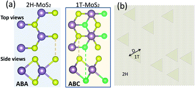 | ||
| Fig. 1 (a) Top and side views of 2H and 1T phases of single-layered MoS2. The 2H and 1T MoS2 show hexagonal lattices with ABA or ABC stacking sequences, respectively. (b) A periodic atomistic model of 2H/1T single-layer MoS2 heterostructure. The 1T or 2H phases inside the heterostructures present triangular geometries18 with a characteristic domain size of “D”. | ||
According to the experimental observations,18 1T or 2H phases inside the heterostructures present triangular geometries18 with a characteristic domain size, which is represented in our study by “D”. In the present investigation, we explored the thermal conductivity of different single-layer MoS2 heterostructures with various combination of 1T and 2H phases and with different characteristic domain sizes as well. Based on the experimental observations,18 between 2H and 1T phases depending on the configuration of heterostructure, 3 different grain boundaries namely; “α”, “β” and “γ” can be formed. The top and side views of atomic structure of these grain boundaries are shown in Fig. 2. In this work, we developed a program to create the atomistic models of these grain boundaries. Depending on the configuration of single-layer MoS2 heterostructure, the arrangement of different grain boundaries in the experimentally synthesized samples change.18 In Fig. 2d, the arrangement of α, β and γ interfaces for 2H inside 1T and vice versa are illustrated.
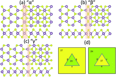 | ||
| Fig. 2 (a–c) Top and side views of atomic structure of “α”, “β” and “γ” interfaces between 2H and 1T phases. (d) Arrangement of different grain boundaries according to the configuration of single-layer MoS2 heterostructure, revealed by the experiment.18 | ||
In this investigation, we explored the thermal conductivity along all-MoS2 heterostructures by developing a combined atomistic-continuum multiscale method.26 In this approach, classical molecular dynamics simulations were carried out to compute thermal conductivities of the pristine 2H and 1T phases and also to acquire the contact conductance along the α, β and γ interfaces. Finally, the properties obtained by the atomistic simulations were used to construct macroscopic samples of MoS2 heterostructures using the finite element method. The details of molecular dynamics and finite element modeling are presented in detail as follows.
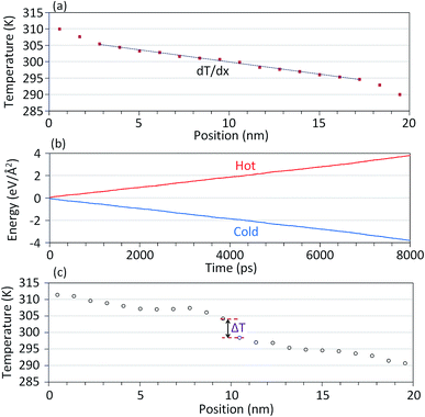
Molecular dynamics calculations in this study were performed using LAMMPS (Large-scale Atomic/Molecular Massively Parallel Simulator)27 package. We used reactive empirical bond order (REBO) potential28,29 for the modeling of atomic interactions in the MoS2 structures. Worthy to note that we found that only ReaxFF25 and REBO28,29 forcefields can keep the constructed MoS2 structures stable. The non-equilibrium molecular dynamics (NEMD) method was employed to study the thermal conduction properties. Time increment of the NEMD simulation for the evaluation of thermal conductivity of the pristine films and thermal conductance of the interface boundaries was set to 0.2 fs and 0.1 fs, respectively. The NEMD modeling performed in this study is very similar to those we used in our recent works.30 In this approach, simulations were performed for samples with different lengths. For each sample, we applied periodic boundary condition along the planar directions to remove the effect of free atoms on the boundaries. All structures were first relaxed and equilibrated at the room temperature (300 K) using the Nosé–Hoover barostat and thermostat (NPT) method for 20 ps. For the NPT method, the damping parameters for the temperature and pressure were set at 10 fs and 100 fs, respectively. Next, several rows of atoms at the two ends were fixed and the structures were further equilibrated using the Nosé–Hoover thermostat method (NVT). The simulation box was divided into several slabs and then as for the loading condition, we applied a temperature difference along the first and last slabs.30 In this case, the temperatures for these two slabs were controlled at the adjusted values using the NVT method, while the rest of the structure were simulated using the constant energy (NVE) method. We remind that the damping parameter for the all NVT steps in this work was set at 10 fs. To keep the imposed temperature difference during the simulation time, it is necessary to apply a constant heat-flux along the system in order to observe the steady-state heat transfer condition. As a result of the imposed temperature difference, a heat-flux is applied on the system by continuously adding energy to the atoms in the hot slab (with higher temperature) and removing energy from the atoms in the cold slab (with lower temperature). The applied heat-flux, qx, can be computed using the following relation:
 | (1) |
 | (2) |
 is constant). For the same sample, the net energy values added or removed from the structure are plotted in Fig. 3b. In this work, the energy values were recorded every 2 fs of simulation time and were averaged for every 40 fs intervals to calculate the applied heat-flux. As illustrated in Fig. 3b, the amount of energy added to the hot reservoir and that removed from the cold reservoir are equal which implies that the total energy of the system is conserved. In addition, slopes of energy curves are linear meaning that the applied heat-flux is constant. According to the applied heat-flux and established temperature gradient, the thermal conductivity of pristine films, k, can be calculated using the one-dimensional form of the Fourier law:
 | (3) |
For the evaluation of thermal contact conductance, the established temperature difference, ΔT due to the presence of grain boundary was considered. In Fig. 3c, a sample of temperature profile along a 1T/2H interface is depicted. As it can be observed, the temperature profile present a clear temperature difference in the middle of the sample where the 1T/2H interface is positioned. The interface conductance, Ci can be computed on the basis of the applied heat-flux, qx and the established temperature difference, ΔT using the following relation:
 | (4) |
Finally, the effective thermal conductivity of heterostructures was obtained using the finite element (FE) method. Finite element modeling in this study were carried out in ABAQUS/standard by using python scripting. For the construction of continuum models of MoS2 heterostructure, according to the volume fraction and domain size of the secondary phase, we randomly distributed 1000 triangles in a square plane with a defined dimension of L. We used the NEMD results for the thermal conductivity of pristine films to introduce the thermal conductivities of each corresponding phase. Moreover, 1T/2H interface conductance values obtained by the NEMD method were used to introduce 1T/2H contact conductance properties in the same orders as those realized experimentally (Fig. 2d).18 In the modeling of thermal contact conductance elements in ABAQUS, one has two separate every two contacting faces. In this work, the master surface was chosen to be the one that is on the original phase and then the other contacting surface on the secondary phase was selected to be the slave surface. We used the free method for the meshing of the constructed heterostructures in ABAQUS using the combination of 3-node (DC2D3) and 4-node (DC2D4) linear heat transfer element types. For the loading condition, positive (inward) and negative (outward) heat-fluxes (hf) were applied on the two opposite surfaces of the constructed models. The temperature of the outer surface of the cold surface (the surface in which the outward heat-flux is applied) was set to zero as the boundary condition. As a result of applied constant heat-flux, a steady-state temperature profile forms along the sample. The temperature difference along the specimen, ΔT was then computed which is proportional to the structure effective thermal conductivity, keff, through:
 | (5) |
3. Results and discussions
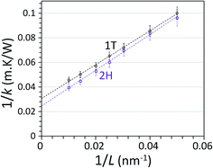
We performed NEMD simulations for the pristine 2H and 1T phases and 1T/2H interfaces for samples with different lengths to explore the length effect on the predicted thermal conduction properties. For the pristine 2H and 1T MoS2, we found increasing trends in the thermal conductivity by increasing the length (L) of the structure. As a common approach, the thermal conductivity of membranes with infinite length can be obtained by extrapolation of results for the samples with finite lengths. A simple approach is to define an effective phonon mean free path (Λeff) as 1/Λeff = 1/Λ + 1/L. Since the thermal conductivity is proportional to Λeff, the thermal conductivity of the infinite system can be obtained by extrapolating to 1/L = 0.31 In Fig. 4, the NEMD results for the inverse of thermal conductivity of defect-free 1T and 2H MoS2 as a function of length inverse are illustrated. According to the explained methodology, we fitted lines to the NEMD results shown in Fig. 4, in order to obtain the thermal conductivity of the sheets with infinite length. This way, the thermal conductivity of pristine 2H and 1T MoS2 at room temperature are calculated to be 40 ± 4 W m−1 K−1 and 32 ± 3 W m−1 K−1, respectively. There have been numerous experimental reports for lattice thermal conductivity of semiconducting MoS2.32,33 In these preliminary experimental works, thermal conductivity of few-layer 2H MoS2 were measured to be 34.5 ± 4 W m−1 K−1 (ref. 32) and ∼52 W m−1 K−1.33 Moreover, recently the thermal conductivity of high-quality bulk 2H MoS2 were experimentally measured to be in a range of 85–110 W m−1 K−1.34 Considering the wide range of experimental results for the thermal conductivity of 2H MoS2, our NEMD results based on the REBO potential yields a thermal conductivity with acceptable accuracy. It should be emphasized that our aim is to study the relative thermal conductivity of all-MoS2 heterostructures and not to exactly report the thermal conductivity. We note that to the best of our knowledge the thermal conductivity of metallic 1T MoS2 has been studied neither experimentally nor theoretically. Based on our NEMD results, the thermal conductivity of 1T MoS2 is only around 20% smaller than that for the 2H MoS2. We also analyzed the length effect on the thermal contact conductance of the 1T/2H grain boundaries and in this case we realized that the length effect is negligible. This can be explained due to the fact that the phonon-defects scattering along the 1T/2H interface as the main factor that determines the thermal resistance, phonon–phonon scattering plays a marginal role here. Based on our classical molecular dynamics modeling, thermal conductance of α, β and γ grain boundaries were obtained to be 0.75 ± 0.1 GW m−2 K−1, 1.1 ± 0.15 GW m−2 K−1 and 0.66 ± 0.1 GW m−2 K−1 respectively.In order to understand the underlying mechanism resulting in different thermal conduction properties along MoS2 structures, we calculated the phonon density of states (PDOS). In this case, we simulate structures at room temperature under the NVE method for 120 ps in which atomic velocities were recorded every 1 fs. By post-processing the trajectories the PDOS were calculated. The PDOS was computed by calculating the Fourier transform of the velocity autocorrelation function, as follows:
 | (6) |
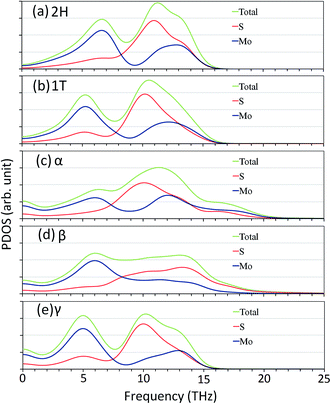 | ||
| Fig. 5 Calculated vibrational phonon density of states (PDOS) for pristine 1T and 2H MoS2 and α, β and γ 1T/2H interfaces. | ||
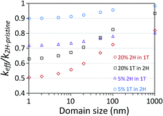
The thermal conductivity of heterostructures strongly correlates to the volume concentration of the additive phase. In this work we studied samples with 5% and 20% concentrations of the secondary phase. We considered only two concentrations of 20% and 5% because they can represent samples with high and medium concentrations, respectively. The main factor that may dominate the heat conduction along the MoS2 heterostructures is the domain size of the secondary phase and such that we considered a wide range from 1 nm to 1000 nm to elaborately discuss this effect. In Fig. 6, the effective thermal conductivity of various MoS2 heterostructures as a function of domain size predicted by the NEMD/FE multiscale approach are illustrated. We reported the normalized thermal conductivity of heterostructures with respect to the thermal conductivity of pristine 2H MoS2 in order to comparatively investigate the heat conduction. As illustrated in Fig. 6, the effective thermal conductivity of MoS2 heterostructures keep increasing by increasing the domain size. This enhancement in the thermal conductivity by increasing the domain size was found to be considerable for the heterostructures with the domain sizes smaller than 100 nm. This finding reveals the considerable importance of the 1T/2H interfaces thermal conductance when the domain sizes are at nanoscale. Since the thermal conductivity of 2H phase is higher than that for 1T MoS2, one may expect higher effective thermal conductivity for the heterostructures with higher concentration of 2H phase inside the 1T. According to our results, this expectation is however valid only for the heterostructures with domain sizes around or higher than 1 μm. In this case, despite of the higher concentration of the phase with superior thermal conductivity (2H phase), the increase in the thermal resistance due to the increase of the 1T/2H interfaces leads to a decline in the effective thermal conductivity, particularly for the heterostructures with domain sizes smaller than 100 nm. This way, based on our multiscale modeling the effect of 1T/2H grain boundary conductance on the thermal conductivity of MoS2 heterostructures become negligible only when the domain sizes are around micrometers. Our multiscale results reveal that the thermal conductivity of MoS2 can be finely tuned by fabrication of heterostructures. Moreover, we predict that in comparison with the pristine 2H phase the thermal conductivity of MoS2 heterostructure cannot be substantially suppressed. This finding is important and reveals that the thermal management of nanodevices made from MoS2 heterostructure may not be considerably declined in comparison with those made only from pristine 2H MoS2.
In Fig. 7, samples of modeling results for the calculated steady-state temperature and heat-flux profiles for MoS2 heterostructures constructed with 20% 1T phase inside 2H MoS2 with domain sizes of 1 nm and 100 nm are compared. For the sample with domain size of 1 nm, the temperature distribution inside 1T phase are found to be primarily constant (Fig. 7d inset) and the temperature changes are mainly occurring at the 1T/2H interfaces. In this case, the secondary 1T triangular domains are almost not participating in the heat-flux transfer (Fig. 7c). Since the 1T/2H interface resistance effect dominates the thermal conductivity for small domain sizes, the heat-flux is transferred only though the original 2H phase and the 1T phase are almost acting as voids. On the other hand, for the heterostructures with large domain sizes, the temperature changes are more uniformly happening throughout the structure (Fig. 7b) which implies that the effect of 1T/2H interface resistance is substantially weakened. In this case, although the 2H phase is more engaged in the heat-flux transfer, the 1T triangles also actively participate in the heat conduction.
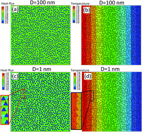 | ||
| Fig. 7 Comparison of the effect of domain size effect on the temperature and heat-flux distributions for MoS2 heterostructures constructed with 20% 1T phase inside 2H MoS2. | ||
4. Conclusion
We proposed a combined atomistic-continuum multiscale modeling to explore the effective thermal conductivity of all-MoS2 single-layer heterostructures. In this approach, non-equilibrium molecular dynamics (NEMD) method was employed to compute the thermal conductivity of pristine semiconducting (2H) and metallic (1T) MoS2 phases and also to calculate the thermal contact conductance between 1T and 2H phases. In order to investigate the effective thermal conductivity of heterostructures at larger scales, we constructed relatively large continuum models of MoS2 heterostructures using the finite element (FE) approach. In this regard, acquired properties by the molecular dynamics simulations were used to introduce thermal conductivity of the representative phases as well as the corresponding interfaces thermal conductance. Our classical modeling results based on the REBO potential for the pristine 2H MoS2 yields a thermal conductivity of around 40 ± 4 W m−1 K−1, with acceptable accuracy as compared with experimental results. Moreover, the thermal conductivity of metallic MoS2 was predicted to be only around 20% smaller than that for the pristine semiconducting MoS2. The thermal conductance of α, β and γ interfaces between 1T and 2H phases were estimated to be 0.75 ± 0.1 GW m−2 K−1, 1.1 ± 0.15 GW m−2 K−1 and 0.66 ± 0.1 GW m−2 K−1, respectively. NEMD/FE multiscale results reveal the significance of 1T/2H interfaces thermal conductance effect when the domain sizes are at nanoscale. It was shown that the effective thermal conductivity of heterostructures increases by increasing the domain size. We explain that the thermal conductivity of MoS2 can be finely tuned by fabrication of heterostructures. More importantly, we predicted that owing to the strong thermal coupling of 1T/2H interfaces the effective thermal conductivity of MoS2 heterostructure remains close to that of pristine 2H phase. This finding reveals that the thermal management of nanodevices made from MoS2 heterostructure would not be declined in comparison with those made from pristine 2H MoS2. In response to the remarkably fast growth and interests in the field of 2D materials, the proposed multiscale approach can be considered to efficiently explore the effective thermal conductivity of various 2D heterostructures.Acknowledgements
BM and TR greatly acknowledge the financial support by European Research Council for COMBAT project (Grant number 615132).References
- K. S. Novoselov, A. K. Geim, S. V Morozov, D. Jiang, Y. Zhang and S. V. Dubonos, et al., Electric field effect in atomically thin carbon films., Science, 2004, 306, 666–669, DOI:10.1126/science.1102896.
- A. K. Geim and K. S. Novoselov, The rise of graphene, Nat. Mater., 2007, 6, 183–191, DOI:10.1038/nmat1849.
- F. Schedin, A. K. Geim, S. V. Morozov, E. W. Hill, P. Blake and M. I. Katsnelson, et al., Detection of individual gas molecules adsorbed on graphene., Nat. Mater., 2007, 6, 652–655, DOI:10.1038/nmat1967.
- A. H. Castro Neto, N. M. R. Peres, K. S. Novoselov, A. K. Geim and F. Guinea, The electronic properties of graphene, Rev. Mod. Phys., 2009, 81, 109–162, DOI:10.1103/RevModPhys.81.109.
- S. Ghosh, W. Bao, D. L. Nika, S. Subrina, E. P. Pokatilov and C. N. Lau, et al., Dimensional crossover of thermal transport in few-layer graphene., Nat. Mater., 2010, 9, 555–558, DOI:10.1038/nmat2753.
- C. Lee, X. Wei, J. W. Kysar and J. Hone, Measurement of the Elastic Properties and Intrinsic Strength of Monolayer Graphene, Science, 2008, 321, 385–388, DOI:10.1126/science.1157996.
- B. Mortazavi, Z. Fan, L. F. C. Pereira, A. Harju and T. Rabczuk, Amorphized graphene: A stiff material with low thermal conductivity, Carbon, 2016, 103, 318–326, DOI:10.1016/j.carbon.2016.03.007.
- G. R. Berdiyorov and M. E. A. Madjet, First-principles study of electronic transport and optical properties of penta-graphene, penta-SiC2 and penta-CN2, RSC Adv., 2016, 6, 50867–50873, 10.1039/c6ra10376f.
- B. Mortazavi, G. Cuniberti and T. Rabczuk, Mechanical properties and thermal conductivity of graphitic carbon nitride: A molecular dynamics study, Comput. Mater. Sci., 2015, 99, 285–289, DOI:10.1016/j.commatsci.2014.12.036.
- A. A. Khatibi and B. Mortazavi, A study on the nanoindentation behaviour of single crystal silicon using hybrid MD-FE method, Adv. Mater. Res., 2008, 32, 259–262 CrossRef CAS.
- K. Watanabe, T. Taniguchi and H. Kanda, Direct-bandgap properties and evidence for ultraviolet lasing of hexagonal boron nitride single crystal, Nat. Mater., 2004, 3, 404–409, DOI:10.1038/nmat1134.
- Y. Kubota, K. Watanabe, O. Tsuda and T. Taniguchi, Deep ultraviolet light-emitting hexagonal boron nitride synthesized at atmospheric pressure, Science, 2007, 317, 932–934, DOI:10.1126/science.1144216.
- L. Song, L. Ci, H. Lu, P. B. Sorokin, C. Jin and J. Ni, et al., Large scale growth and characterization of atomic hexagonal boron nitride layers, Nano Lett., 2010, 10, 3209–3215, DOI:10.1021/nl1022139.
- L. Liu, J. Park, D. a. Siegel, K. F. McCarty, K. W. Clark and W. Deng, et al., Heteroepitaxial Growth of Two-Dimensional Hexagonal Boron Nitride Templated by Graphene Edges, Science, 2014, 343, 163–167, DOI:10.1126/science.1246137.
- Z. Liu, L. Ma, G. Shi, W. Zhou, Y. Gong and S. Lei, et al., In-plane heterostructures of graphene and hexagonal boron nitride with controlled domain sizes, Nat. Nanotechnol., 2013, 8, 119–124, DOI:10.1038/nnano.2012.256.
- B. Radisavljevic, A. Radenovic, J. Brivio, V. Giacometti and A. Kis, Single-layer MoS2 transistors, Nat. Nanotechnol., 2011, 6, 147–150, DOI:10.1038/nnano.2010.279.
- Q. H. Wang, K. Kalantar-Zadeh, A. Kis, J. N. Coleman and M. S. Strano, Electronics and optoelectronics of two-dimensional transition metal dichalcogenides, Nat. Nanotechnol., 2012, 7, 699–712, DOI:10.1038/nnano.2012.193.
- Y.-C. Lin, D. O. Dumcenco, Y.-S. Huang and K. Suenaga, Atomic mechanism of the semiconducting-to-metallic phase transition in single-layered MoS2, Nat. Nanotechnol., 2014, 9, 391–396, DOI:10.1038/nnano.2014.64.
- L. F. Mattheiss, Band structures of transition-metal-dichalcogenide layer compounds, Phys. Rev. B: Condens. Matter Mater. Phys., 1973, 8, 3719–3740, DOI:10.1103/PhysRevB.8.3719.
- F. Wypych and R. Schöllhorn, 1T-MoS2, a new metallic modification of molybdenum disulfide, J. Chem. Soc., Chem. Commun., 1992, 1386–1388 RSC.
- Y. Gao, Q. Liu and B. Xu, Lattice Mismatch Dominant Yet Mechanically Tunable Thermal Conductivity in Bilayer Heterostructures, ACS Nano, 2016, 10, 5431–5439, DOI:10.1021/acsnano.6b01674.
- M.-H. Chiu, C. Zhang, H.-W. Shiu, C.-P. Chuu, C.-H. Chen and C. Y. S. Chang, et al., Determination of band alignment in the single-layer MoS2/WSe2 heterojunction, Nat. Commun., 2015, 6, 7666, DOI:10.1038/ncomms8666.
- R. Ganatra and Q. Zhang, Few-layer MoS2: A promising layered semiconductor, ACS Nano, 2014, 8, 4074–4099, DOI:10.1021/nn405938z.
- N. B. Le, T. D. Huan and L. M. Woods, Interlayer Interactions in van der Waals Heterostructures: Electron and Phonon Properties, ACS Appl. Mater. Interfaces, 2016, 8, 6286–6292, DOI:10.1021/acsami.6b00285.
- B. Mortazavi, A. Ostadhossein, T. Rabczuk and A. C. T. van Duin, Mechanical response of all-MoS2 single-layer heterostructures: a ReaxFF investigation, Phys. Chem. Chem. Phys., 2016, 18, 23695–23701, 10.1039/c6cp03612k.
- B. Mortazavi, J. Bardon, J. A. S. Bomfim and S. Ahzi, A statistical approach for the evaluation of mechanical properties of silica/epoxy nanocomposite: Verification by experiments, Comput. Mater. Sci., 2012, 59, 108–113, DOI:10.1016/j.commatsci.2012.03.002.
- S. Plimpton, Fast Parallel Algorithms for Short-Range Molecular Dynamics, J. Comput. Phys., 1995, 117, 1–19, DOI:10.1006/jcph.1995.1039.
- T. Liang, S. R. Phillpot and S. B. Sinnott, Parametrization of a reactive many-body potential for Mo–S systems, Phys. Rev. B: Condens. Matter Mater. Phys., 2009, 79, 245110 CrossRef.
- K. Q. Dang, J. P. Simpson and D. E. Spearot, Phase transformation in monolayer molybdenum disulphide (MoS2) under tension predicted by molecular dynamics simulations, Scr. Mater., 2014, 76, 41–44, DOI:10.1016/j.scriptamat.2013.12.011.
- B. Mortazavi, O. Rahaman, T. Rabczuk and L. F. C. Pereira, Thermal conductivity and mechanical properties of nitrogenated holey graphene, Carbon, 2016, 106, 1–8, DOI:10.1016/j.carbon.2016.05.009.
- P. K. Schelling, S. R. Phillpot and P. Keblinski, Comparison of atomic-level simulation methods for computing thermal conductivity, Phys. Rev. B: Condens. Matter Mater. Phys., 2002, 65, 1–12, DOI:10.1103/PhysRevB.65.144306.
- R. Yan, J. R. Simpson, S. Bertolazzi, J. Brivio, M. Watson and X. Wu, et al., Thermal conductivity of monolayer molybdenum disulfide obtained from temperature-dependent Raman spectroscopy, ACS Nano, 2014, 8, 986–993, DOI:10.1021/nn405826k.
- S. Sahoo, A. P. S. Gaur, M. Ahmadi, M. J. F. Guinel and R. S. Katiyar, Temperature-dependent Raman studies and thermal conductivity of few-layer MoS2, J. Phys. Chem. C, 2013, 117, 9042–9047, DOI:10.1021/jp402509w.
- J. Liu, G. M. Choi and D. G. Cahill, Measurement of the anisotropic thermal conductivity of molybdenum disulfide by the time-resolved magneto-optic Kerr effect, J. Appl. Phys., 2014, 116, 4904513 Search PubMed.
| This journal is © The Royal Society of Chemistry 2017 |

