
 Open Access Article
 This Open Access Article is licensed under a Creative Commons Attribution-Non Commercial 3.0 Unported Licence
Reproducible and reliable resistive switching behaviors of AlOX/HfOX bilayer structures with Al electrode by atomic layer deposition†
Masoud Akbari‡
,
Min-Kyu Kim‡,
Dongshin Kim and
Jang-Sik Lee *
*
Department of Materials Science and Engineering, Pohang University of Science and Technology (POSTECH), Pohang 790-784, Republic of Korea. E-mail: jangsik@postech.ac.kr
First published on 15th March 2017
Abstract
The resistive switching behaviors of AlOX/HfOX bilayer structures were investigated. Metal oxides were deposited by atomic layer deposition. Al and Pt were used as top and bottom electrodes, respectively. Compared with AlOX and HfOX monolayer structures, the bilayer structure showed lower set/reset voltages and more-uniform resistive switching properties. It also exhibited good data retention and endurance. The Al top electrode may gather oxygen ions from the oxide layer underneath and thereby create oxygen vacancies in the oxide layer. The uniform electrical property of the bilayer structure is attributed to confined formation/rupture of conductive filaments in the HfOX layer, whereas undissociated filaments in the AlOX layer nucleate rapid regeneration of filaments.
Introduction
Conventional charge-based memories are approaching their scaling limit, so alternative memory architectures are required. Resistive random access memory (RRAM) is one of the most promising candidates for next generation non-volatile memory devices due to its features, such as simple device structure, fast switching speed, and low power consumption.1 Among various materials that have been studied, transition metal oxides such as SrTiOX, TiOX, ZrOX, AlOX, HfOX, etc. have suitable performance in terms of resistive switching parameters.2–8 In particular, RRAM based on these materials without active metal electrode have been called as valence change memory (VCM). Previous studies indicate that the resistive switching mechanism in VCM originates from migration of oxygen ions, whereby oxygen vacancies form a conductive filament under voltage sweep and consequently make the device switch from high-resistance state (HRS) to low-resistance state (LRS).9,10Atomic layer deposition (ALD) is a thin film deposition technique that is widely used in semiconductor device fabrication.11 ALD has unique characteristics, including a self-limiting deposition process, excellent conformality, atomic-scale thickness and composition control, and low-temperature deposition. ALD is typically used to deposit dielectric layers for MOSFETs and dynamic random access memory. These applications require a stoichiometric composition with ultra-low leakage current.12
An oxygen-deficient thin film is required for RRAM applications, so ALD process conditions need to be modified, or device structures need to be manipulated. To change the chemical composition of the film, some research groups have tried to change the ALD deposition conditions and recipes, e.g., by altering the time duration of precursor exposure,13 adjusting the mixture of oxidizer and inert gas,14 conducting plasma treatment during deposition,15 and changing substrate temperature.13 However, modifying ALD conditions can cause deviation from the ALD window and degradation of properties of the film.16
As another approach, numerous studies have focused on manipulation of device structures by incorporating a chemically-active layer,17,18 by doping,19,20 and by using bilayer5,21–23 and trilayer structures.24 Due to fabrication simplicity to make bilayer RRAM, different structures have been studied, such as ZrOX/HfOX21 and WOX/NbOX.25 Inserting an Al layer between electrode and HfOX improves the switching uniformity, possibly by stabilizing the conductive filaments.26 Moreover, HfOX/AlOX bilayer stacks are capable of multilevel resistive switching.27 In TiN/HfO2/Hf cells, embedding a thin Al2O3 at the TiN/HfO2 or at the Hf/HfO2 interface increases the memory window by increasing the concentration of defects.28 Nevertheless, precise comparison of the resistive switching mechanism in such a bilayer device with those in monolayers remains necessary.
In this paper, we investigated resistive switching behavior of an AlOX/HfOX bilayer structure deposited by ALD. The bilayer structure had uniform memory characteristics and good endurance properties; the uniform resistive switching behavior of bilayer structure emanates from partial dissociation of conductive filaments in the HfOX layer, whereas they remain stable in the AlOX layer during subsequent switching cycles.
Experimental
To fabricate the monolayer structures, a Ti adhesion layer (10 nm) was deposited on SiO2/Si substrate using an electron beam evaporator. Then a Pt bottom electrode (100 nm) was deposited by sputtering. 5 nm AlOX or HfOX were deposited by ALD at 300 °C using trimethylaluminum (TMA) or tetrakis(ethylmethylamino)hafnium (TEMAHf) as precursors, respectively. For both oxides, H2O was used as the oxidizer and Ar as the purging gas. Finally, circular 100 nm-thick Al top electrodes with diameter of 50 μm were deposited on top of the oxide layer by e-beam evaporation through a metal shadow mask. In case of bilayer structures, after deposition of Ti adhesion layer and Pt bottom electrode, 3 nm HfOX was first deposited, followed by 3 nm AlOX. The thickness of oxide was controlled by cycles of ALD and determined using spectroscopic ellipsometer (J.A. Woollam Co., M-2000_D). Then Al top electrodes were deposited on the oxide layers. The current–voltage (I–V) curve were measured using a Semiconductor Characterization System (KEITHLEY, 4200-SCS). The resistive switching speed and pulse response were measured using a waveform generator (33621A, KEYSIGHT) and oscilloscope (TDS 5054, TEKTRONIX). The response time of devices was tested by applying a single set or reset pulse to the device from a waveform generator. Then an I–V sweep with the semiconductor parameter analyzer was conducted to determine the device states. During electrical characterization the bottom electrode was grounded and voltage was applied to the top electrode. All measurements were performed at room temperature in ambient conditions, except the data retention measurement, which was performed at 85 °C. The X-ray photoelectron spectroscopy (XPS) depth profile of AlOX/HfOX bilayer structure was analysed with X-ray photoelectron spectrometer (ESCA LAB250, VG SCIENTIFIC) using a monochromatic Al X-ray source (1486.6 eV) and Ar ion etching. The binding energies were calibrated by the C 1s peak at 284.8 eV. The crystal structure of AlOX/HfOX bilayer was measured using X-ray diffraction (XRD, Rigaku D/MAX-2500) with Cu Kα radiation.Results and discussion
Single AlOX device
Fig. 1 shows the resistive switching behaviors of Al/AlOX/Pt device repeatedly measured for 50 cycles. The device was initially in HRS. To trigger resistive switching from HRS to LRS for the pristine devices, ∼4 V electroforming voltage was needed. The device switched from HRS to LRS when positive voltage was applied, then returned to HRS during negative voltage sweeping; this behavior is known as bipolar resistive switching. Formation of conductive filaments under applied voltage bias is responsible for resistive switching in transition metal oxides.9 Several studies have proven that top electrode element has an impact on memory performance.17,29 The Al top electrode has high affinity for oxygen, and therefore functions as a reservoir of oxygen ions. Oxygen ions in the oxide layer migrate toward the top electrode interface under positive bias, and consequently leave oxygen vacancies in the oxide layer. These vacancies form a conductive filament during the set process. When negative voltage is applied during the reset process, oxygen ions drift back into the oxide layer and recombine with vacancies; thus the filament dissociates and the device switches from LRS to HRS.30 | ||
| Fig. 1 (a) Typical I–V curves of RRAM devices with Al/AlOX/Pt structure. Schematic representation of resistive switching mechanism for (b) low resistance state (LRS), and (c) high resistance state (HRS). | ||
According to the I–V curves (Fig. 1(a)), the device has a very sharp set and reset and also the ON/OFF ratio is relatively large. Moreover, current level at LRS is high. This behavior is similar to resistive switching behavior of conductive-bridge RAM (CBRAM) in which formation and rupture of a metallic filament causes sharp set/reset.31 Bearing in mind that the device in our study is not a CBRAM, we can speculate that the above-mentioned behavior is due to formation/rupture of a very thick and dense filament made from oxygen vacancy (Fig. 1(b)). The AlOX layer might contain a large number of oxygen vacancies, which are created during deposition or through contact with Al top electrode. Under electric field, oxygen vacancies form a thick and dense filament, consequently, resistance significantly reduces and device switches to LRS. During negative bias dissociation of such a dense filament results in a sharp reset to HRS (Fig. 1(c)).
Single HfOX device
In order to make a comparison, we changed the switching layer to HfOX deposited by ALD. Typical I–V curves of are shown in Fig. 2(a). Compared to AlOX device, electrical properties deteriorated. However, it is worthy of consideration that the repeating I–V curves fall into two main groups, one in which reset is sharp and resistance change is large (similar to I–V curves of AlOX device), and one in which reset is gradual and resistance change is low. These diverse switching cycles occur quite randomly during repeating voltage sweep.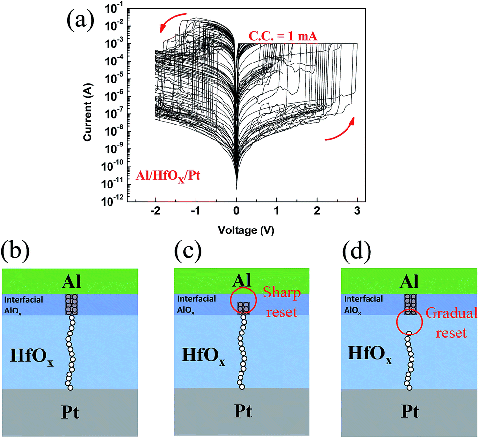 | ||
| Fig. 2 (a) Typical I–V curves of RRAM devices with Al/HfOX/Pt structure. Schematic representation of resistive switching mechanism for (b) LRS, (c) HRS with sharp reset, and (d) HRS with gradual reset. | ||
The presence of these two behaviors can be explained in terms of formation of a non-uniform filament. Since Al is chemically active, an interfacial AlOX layer is formed between electrode and HfOX layer.30,32 Accordingly, we can consider the device structure as a bilayer AlOX/HfOX that the formed filament in each layer might be dissimilar (Fig. 2(b)). By comparing the I–V characteristics of AlOX and HfOX, we suggest that filament in interfacial AlOX layer might be larger than the one in HfOX layer; therefore, during reset process if the thick filament in interfacial AlOX is dissociated, resistance sharply reduces and device goes to very low resistance state (Fig. 2(c)). Likewise, if the weak filament in HfOX layer is ruptured, reset is gradual and resistance change is lower (Fig. 2(d)).
Bilayer AlOX/HfOX device
The randomness of the observed different switching in HfOX device can be due to instability of filament in both oxides. Considering the thick and dense filament in AlOX device on the one hand, and two different HRS levels in HfOX device on the other hand, we intentionally deposited bilayer AlOX/HfOX device by ALD. The bilayer structure of AlOX/HfOX/Pt was confirmed by XPS depth profile (Fig. S1(a)†). When devices were fabricated with AlOX/HfOX bilayer structure, 3 nm of each layer was chosen for lower operation voltages as well as reliable operation. The crystal structure of AlOX/HfOX layer was measured by XRD. As shown in Fig. S1(b),† there is only Pt (111) peak and any peaks of AlOX/HfOX layer were not found. This result may indicate that AlOX/HfOX bilayer is amorphous, but further study using high resolution electron microscopy needs to be done to clarify the crystallization nature. Typical I–V curves are shown in Fig. 3(a). Interestingly, bilayer device shows uniform resistive switching during repeated cycles and low set/reset voltages with a gradual reset process. The schematic representation of resistive switching mechanism in the bilayer AlOX/HfOX device is shown in Fig. 3(b and c). Filament that forms in AlOX layer is proportionately thick and stable while in HfOX layer is weak (Fig. 3(b)), so during the reset process only the weak filaments in the HfOX layer dissociate (Fig. 3(c)). The undissociated filaments in the AlOX layer nucleate regrowth of filaments during the next set process.33 This process reduces the randomness of formation of filament and consequently improves the uniformity of resistive switching in the bilayer structure. Analogous to this mechanism, some studies have suggested partial formation/rupture of filaments in other bilayer RRAM devices.25,34 Fig. 4(a) shows distribution of set voltages of devices. The bilayer device showed more uniform resistive switching during repeated cycles than the monolayer devices. The AlOX/HfOX bilayer structure had significantly more uniform resistance of LRS/HRS than the monolayer devices (Fig. 4(b)). In practical application, broad distribution of RRAM parameters such as operation voltages and resistance in HRS and LRS has been issues.35 In this view, this method to improve the uniformity of RRAM devices can be a good solution.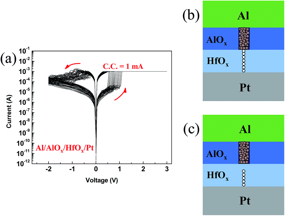 | ||
| Fig. 3 (a) Typical I–V curves of RRAM devices with AlOX/HfOX bilayer structure. Schematic representation of resistive switching mechanism for (b) LRS and (c) HRS, respectively. | ||
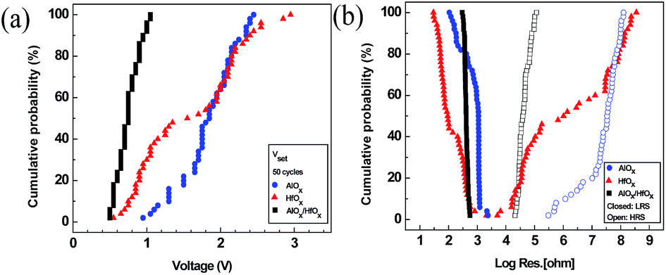 | ||
| Fig. 4 Cycle-to-cycle cumulative probability distribution of (a) set/reset voltages and (b) LRS/HRS resistance states. | ||
In order to verify controllability of filament further, we applied different negative voltage in reset process (Fig. 5(a)). Due to the gradual reset process in the AlOX/HfOX bilayer structure, selecting different stop points (−1.5, −2 and −2.5 V) will lead to create diverse HRS levels (HRS 1–3#). The magnitude of HRS level depends on the proportion of filament that dissociates under negative electric field (Fig. 5(b–d)). When reset stop point is small (−1 V) a slight amount of filament in HfOX layer dissolves and consequently resistance change will be low. The higher negative voltage is applied, the lower HRS level will be achieved. Besides, filament in AlOX layer remains stable. This indicates that such a bilayer structure brings about controllability of filament, as well as the ability to modify resistive switching behavior. Good endurance properties and data retention are essential in non-volatile memory applications. To estimate the electrical reliability of our devices, endurance properties and data retention were measured. In endurance test, set voltage pulse (+4 V, 10 ms) and reset voltage pulse (−3 V, 10 ms) were used (Fig. S2†). The bilayer structure showed some fluctuations in HRS during endurance cycles, but resistive switching maintained stable for more than 400 cycles, whereas AlOX and HfOX devices failed after around 170 and 220 cycles, respectively (Fig. 6(a)). Data retention tests of the bilayer structure were conducted at 85 °C. The device remained stable without any noticeable degradation (Fig. 6(b)). Similar data retention property was also observed at room temperature. Further improvement of endurance and data retention properties is being done based on this study by the optimization of various process conditions and device dimension scaling.
 | ||
| Fig. 5 (a) Typical I–V curves of AlOX/HfOX bilayer structure measured at different reset stop voltages to show controllability of filament. (b–d) Schematic representation of resistive switching mechanism for 3 different HRS #1–3, respectively. | ||
 | ||
| Fig. 6 (a) Pulse endurance test of AlOX/HfOX bilayer structures. (b) Data retention characteristics of AlOX/HfOX bilayer structure at 85 °C. | ||
We measured switching speed of RRAM device with AlOX/HfOX bilayer structure. When we applied 100 ns pulse with amplitude of 2 V, the state of devices was changed from HRS to LRS. The state of devices was confirmed by dc voltage sweep before and after applying bias pulses (Fig. S3(a)†). In the same way, reset process is confirmed by applying 100 ns pulse with amplitude of −3 V (Fig. S3(b)†). The 100 ns pulse width was enough to switch the resistance state of devices. In addition resistive switching behavior in pulse mode verified by set–read–reset–read pulse cycle tests (Fig. S3(c)†).
Conclusions
In conclusion, we investigated the resistive switching behaviors of AlOX/HfOX bilayer structures. By using Al as the top electrode and AlOX/HfOX bilayer structures, memory devices had reproducible and reliable resistive switching operations, good endurance, and good data retention properties. We suggest that the uniform and reliable switching behaviors may be due to confined formation and dissociation of filaments in the bilayer structures; i.e. filaments in HfOX layer are weak and they form/dissociate during set/reset, while filaments in AlOX layer are thick, and they remain stable during set/reset. The undissociated filaments in the AlOX layer facilitate the nucleation and regrowth of filament in HfOX layer. This study provides an easy ALD process to fabricate reliable resistive switching memory devices with simple device structures for potential application to future nonvolatile memory industry.Acknowledgements
This work was supported by National Research Foundation of Korea (NRF-2016M3D1A1027663, NRF-2015R1A2A1A15055918). This work was also supported by Future Semiconductor Device Technology Development Program (10045226) funded by the Ministry of Trade, Industry & Energy (MOTIE)/Korea Semiconductor Research Consortium (KSRC). In addition, this work was partially supported by Brain Korea 21 PLUS project (Center for Creative Industrial Materials).Notes and references
- R. Waser, R. Dittmann, G. Staikov and K. Szot, Adv. Mater., 2009, 21, 2632–2663 CrossRef CAS.
- H.-S. Wong, H.-Y. Lee, S. Yu, Y.-S. Chen, Y. Wu, P.-S. Chen, B. Lee, F. T. Chen and M.-J. Tsai, Proc. IEEE, 2012, 100, 1951–1970 CrossRef CAS.
- Y. Huang, Z. H. Shen, Y. Wu, X. Q. Wang, S. F. Zhang, X. Q. Shi and H. B. Zeng, RSC Adv., 2016, 6, 17867–17872 RSC.
- Y. Huang, Z. H. Shen, Y. Wu, M. Q. Xie, Y. Q. Hu, S. F. Zhang, X. Q. Shi and H. B. Zeng, AIP. Adv., 2016, 6, 025018 CrossRef.
- M.-K. Kim and J.-S. Lee, ACS Appl. Mater. Interfaces, 2016, 8, 32918–32924 CAS.
- K. Park and J.-S. Lee, Nanotechnology, 2016, 27, 125203 CrossRef PubMed.
- U. B. Han and J. S. Lee, Sci. Rep., 2016, 6, 25537 CrossRef CAS PubMed.
- U. B. Han and J. S. Lee, Sci. Rep., 2016, 6, 28966 CrossRef CAS PubMed.
- C.-Y. Lin, C.-Y. Wu, C.-Y. Wu, C. Hu and T.-Y. Tseng, J. Electrochem. Soc., 2007, 154, G189–G192 CrossRef CAS.
- S. Long, X. Lian, C. Cagli, X. Cartoixa, R. Rurali, E. Miranda, D. Jiménez, L. Perniola, M. Liu and J. Suñé, Appl. Phys. Lett., 2013, 102, 183505 CrossRef.
- H. Kim, H.-B.-R. Lee and W.-J. Maeng, Thin Solid Films, 2009, 517, 2563–2580 CrossRef CAS.
- S. M. George, Chem. Rev., 2009, 110, 111–131 CrossRef PubMed.
- J. J. Yang, N. P. Kobayashi, J. P. Strachan, M.-X. Zhang, D. A. Ohlberg, M. D. Pickett, Z. Li, G. Medeiros-Ribeiro and R. S. Williams, Chem. Mater., 2010, 23, 123–125 CrossRef.
- S.-J. Park, J.-P. Lee, J. S. Jang, H. Rhu, H. Yu, B. Y. You, C. S. Kim, K. J. Kim, Y. J. Cho and S. Baik, Nanotechnology, 2013, 24, 295202 CrossRef PubMed.
- T.-H. Jung, J.-S. Park, D.-H. Kim, Y. Jeong, S.-G. Park and J.-D. Kwon, J. Vac. Sci. Technol., A, 2013, 31, 01A124 Search PubMed.
- R. A. Fischer, Precursor chemistry of advanced materials: CVD, ALD and nanoparticles, Springer, 2005 Search PubMed.
- H. Y. Jeong, J. Y. Lee and S. Y. Choi, Adv. Funct. Mater., 2010, 20, 3912–3917 CrossRef CAS.
- Y. Wu, B. Lee and H.-S. Philip Wong, IEEE Electron Device Lett., 2010, 31, 1449–1451 CrossRef CAS.
- C.-S. Peng, W.-Y. Chang, Y.-H. Lee, M.-H. Lin, F. Chen and M.-J. Tsai, Electrochem. Solid-State Lett., 2012, 15, H88–H90 CrossRef CAS.
- M. Akbari and J. S. Lee, RSC Adv., 2016, 6, 21917–21921 RSC.
- J. Lee, E. M. Bourim, W. Lee, J. Park, M. Jo, S. Jung, J. Shin and H. Hwang, Appl. Phys. Lett., 2010, 97, 172105 CrossRef.
- J.-K. Lee, S. Jung, J. Park, S.-W. Chung, J. S. Roh, S.-J. Hong, I. H. Cho, H.-I. Kwon, C. H. Park and B.-G. Park, Appl. Phys. Lett., 2012, 101, 103506 CrossRef.
- K. Park and J. S. Lee, RSC Adv., 2016, 6, 21736–21741 RSC.
- L. G. Wang, X. Qian, Y. Q. Cao, Z. Y. Cao, G. Y. Fang, A. D. Li and D. Wu, Nanoscale Res. Lett., 2015, 10, 1–8 CrossRef PubMed.
- S. M. Sadaf, X. Liu, M. Son, S. Park, S. H. Choudhury, E. Cha, M. Siddik, J. Shin and H. Hwang, Phys. Status Solidi A, 2012, 209, 1179–1183 CrossRef CAS.
- S. Yu, B. Gao, H. Dai, B. Sun, L. Liu, X. Liu, R. Han, J. Kang and B. Yu, Electrochem. Solid-State Lett., 2010, 13, H36–H38 CrossRef CAS.
- S. Yu, Y. Wu and H.-S. P. Wong, Appl. Phys. Lett., 2011, 98, 103514 CrossRef.
- L. Goux, A. Fantini, B. Govoreanu, G. Kar, S. Clima, Y.-Y. Chen, R. Degraeve, D. Wouters, G. Pourtois and M. Jurczak, Electrochem. Solid-State Lett., 2012, 1, P63–P65 CrossRef CAS.
- H. Y. Jeong, S. K. Kim, J. Y. Lee and S.-Y. Choi, J. Electrochem. Soc., 2011, 158, H979–H982 CrossRef CAS.
- C. Chen, S. Gao, F. Zeng, G. Tang, S. Li, C. Song, H. Fu and F. Pan, J. Appl. Phys., 2013, 114, 014502 CrossRef.
- I. Valov, R. Waser, J. R. Jameson and M. N. Kozicki, Nanotechnology, 2011, 22, 254003 CrossRef PubMed.
- M. Hota, C. Mukherjee, T. Das and C. Maiti, ECS J. Solid State Sci. Technol., 2012, 1, N149–N152 CrossRef CAS.
- S. Yu, Y. Wu, Y. Chai, J. Provine and H.-S. Wong, Presented in part at the Symposium on VLSI Technology, Systems and Applications (VLSI-TSA), Hsinchu, 25–27 April 2011 Search PubMed.
- H. Lv, H. Wan and T. Tang, IEEE Electron Device Lett., 2010, 31, 978–980 CrossRef CAS.
- S. W. Ryu, S. Cho, J. Park, J. Kwac, H. J. Kim and Y. Nishi, Appl. Phys. Lett., 2014, 105, 072102 CrossRef.
Footnotes |
| † Electronic supplementary information (ESI) available. See DOI: 10.1039/c6ra26872b |
| ‡ These authors contributed equally to this work. |
| This journal is © The Royal Society of Chemistry 2017 |