
 Open Access Article
 This Open Access Article is licensed under a
 Creative Commons Attribution 3.0 Unported Licence
Chemical manipulation of edge-contact and encapsulated graphene by dissociated hydrogen adsorption
S. J. Hong†
a,
H. Kimb,
M. Leec,
H. Kanga,
M. Parka,
D. H. Jeong c,
S. W. Leed,
Y. W. Park*a and
B. H. Kim*e
c,
S. W. Leed,
Y. W. Park*a and
B. H. Kim*e
aDepartment of Physics and Astronomy, Seoul National University, Seoul 08826, Korea. E-mail: ywpark@snu.ac.kr
bKorea Research Institute of Standards and Science (KRISS), Daejeon 34113, Korea
cDepartment of Chemistry Education, Seoul National University, Seoul 08826, Korea
dDepartment of Physics, Ewha Womans University, Seoul, 03760, Korea
eDepartment of Physics, Incheon National University, Incheon 22012, Korea. E-mail: kbh37@inu.ac.kr
First published on 18th January 2017
Abstract
Due to its important role in the mass production of electronics, chemical functionalization is commonly utilized during the development of graphene-based electronics. Dramatically improved graphene devices with encapsulated edge-contact configurations represent an additional application of a suitable functionalization process. In this study, we report the partial functionalization of a novel device by dissociative hydrogen adsorption. We investigate the H2 adsorption process, which results in a change in the electrical properties using an encapsulated edge-contact device. When using chemical functionalization, we found that hydrogenation allows the realization of high-quality two-dimensional material-based electronics.
1. Introduction
The van der Waals (vdW) heterostructure has been extensively studied because several viable combinations of two-dimensional (2D) materials are expected to be able to contribute to improving different electronic properties.1 A prototypical example is the graphene and hexagonal boron nitride (h-BN) heterostructure to realize a high-mobility device.2 h-BN, characterized by a smooth surface, the absence of dangling bonds, and an atomic lattice structure similar to that of graphene, is suitable for use as the basic building block of the graphene-based vdW heterostructure. h-BN has also been utilized for the encapsulation of graphene (e.g. h-BN/graphene/h-BN) to prevent its degradation due to exposure to ambient conditions. Indeed, it has been reported that encapsulation contributes to the electrical stability of graphene devices.3,4 The encapsulated configuration can be extended to other 2D materials which are extremely sensitive to air as well.5Furthermore, the encapsulated configuration has introduced the novel concept of electrical contact to form an atomic contact of carbon to a metal electrode.6 As a result, the electronic performance has been enhanced to its theoretical limits. Wang et al. reported that the mobility of graphene reached 140![[thin space (1/6-em)]](https://www.rsc.org/images/entities/char_2009.gif) 000 cm2 V−1 s−1 at room temperature.6 The maximum mean free path (MFP) is linearly dependent on the size of the device up to 15 μm. This indicates that the MFP has not reached its intrinsic impurity-limited scattering length. Furthermore, the contact resistance, i.e., an interruption in high-performance electronic devices, was reduced to 150 Ω μm. Owing to these advantages, the encapsulated configuration is expected to be a prototype of a high-quality 2D electronic device. In order to develop this novel concept of an electronic device to the point of application, chemical manipulation may be feasible due to its compatibility with mass-production. In this regard, the tight interface of the vdW heterostructure3 must be overcome. Therefore, it is necessary to explore the intercalation, adsorption, and doping of molecules in h-BN/graphene/h-BN devices so as to make chemical manipulation a viable approach.
000 cm2 V−1 s−1 at room temperature.6 The maximum mean free path (MFP) is linearly dependent on the size of the device up to 15 μm. This indicates that the MFP has not reached its intrinsic impurity-limited scattering length. Furthermore, the contact resistance, i.e., an interruption in high-performance electronic devices, was reduced to 150 Ω μm. Owing to these advantages, the encapsulated configuration is expected to be a prototype of a high-quality 2D electronic device. In order to develop this novel concept of an electronic device to the point of application, chemical manipulation may be feasible due to its compatibility with mass-production. In this regard, the tight interface of the vdW heterostructure3 must be overcome. Therefore, it is necessary to explore the intercalation, adsorption, and doping of molecules in h-BN/graphene/h-BN devices so as to make chemical manipulation a viable approach.
Hydrogen is an attractive element to functionalize carbon atom, as it yields stable chemical C–H bonds. With different approaches, various electronic properties have been observed in graphene-based materials modified by hydrogen.7–10 For example, the hydrogenation of graphene-based materials results in a metal–insulator transition,7 electron doping,8,9 and the realization of atomic magnets in local regions.10 The hydrogenation has been applied for improvement of graphene device. At first, the studies were performed on bare SiO2 substrate.7–9 With the help of the h-BN substrate, the hydrogenation has been applied to high-quality graphene device and revealed its intrinsic effects on graphene.11 For ultimate device configuration, h-BN/graphene/h-BN, few researches have been achieved and it is even unclear whether hydrogen molecules can be intercalated or not. Meanwhile, the recent report in which a high-pressure H2 environment has shown the successful intercalation of molecules between graphene layers in graphite12 provides the evidence of the feasibility of chemical manipulation in the vdW structure of h-BN/graphene/h-BN.
Here, we investigate the hydrogenation in the h-BN/graphene/h-BN heterostructure and report the successful intercalation and modification of electrical properties. A vdW heterostructure was fabricated using chemical vapor deposition (CVD)-grown single-layer graphene (SLG) with exfoliated h-BN flakes, yielding a high-quality edge-contact configuration. The intercalation and adsorption of dissociative hydrogen in the vdW structure were revealed by Raman spectroscopy. The adsorption met the requirements of the first-order adsorption model and resulted in electron doping, short-range scattering, and a reduction of the contact resistance. Furthermore, we confirmed the maintenance of these properties even under a high vacuum environment. The hydrogenation of an edge-contact graphene device is expected to contribute to the realization of the chemical manipulation of high-quality graphene-based electronics for mass production.
2. Experimental
SLG was grown by the CVD method13 and h-BN was exfoliated from a commercial crystal component (HQ graphene). We used a wet etching transfer method with a 0.1 M NaOH solution to form the h-BN/SLG/h-BN heterostructure. Thereafter, a conventional lithography process was carried out with bubble and wrinkle-free regions. Raman spectroscopy was also utilized with a 532 nm-wavelength laser, and three-terminal electrical measurements were carried out using a Keithley 4200-SCS parameter analyzer. We obtained a pristine encapsulated device which was annealed at 380 K under 5 × 10⁻⁶ Torr for 10 h in a custom-made high-pressure chamber. After annealing, in situ electrical measurements were taken at 350 K under H2 (99.9999%) at 11 bar of pressure.3. Results and discussion
The CVD-grown SLG was transferred onto the exfoliated h-BN flake on SiO2/Si substrate by the bubbling transfer method.14 The SLG and h-BN are depicted by the white and orange dashed lines, respectively, in Fig. 1(a). Another h-BN flake depicted by the orange dashed line in Fig. 1(b) was transferred onto the SLG/h-BN, yielding the h-BN/SLG/h-BN heterostructure, as shown in Fig. 1(c). Using reactive ion etching (R.I.E.) with a mixture of O2 and CF4, we designed the rectangular heterostructure depicted by the red dashed line in Fig. 1(c). Finally, the edge contact was created by conventional electron beam lithography and metal evaporation (Cr/Au = 3/50 nm), as shown in Fig. 1(d). Fig. 1(e) and (f) indicate a schematic and an atomic force microscopy (AFM) image of the edge-contact device, respectively.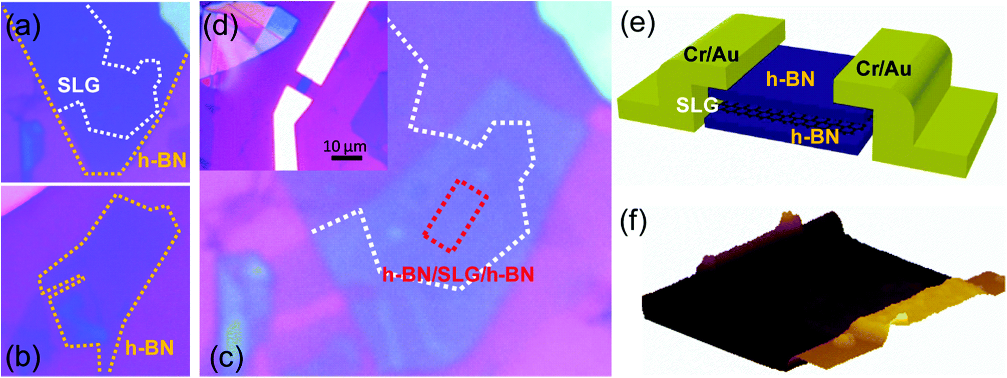 | ||
| Fig. 1 Encapsulated edge-contact vdW heterostructure fabrication process. Optical image of (a) CVD-grown SLG on h-BN flake (b) h-BN flake for covering SLG/h-BN (c) h-BN/SLG/h-BN heterostructure (d) as-fabricated device, respectively. (e) and (f) indicate schematic and AFM image, respectively. | ||
The Raman spectra of the center and edge regions, designated by the red and orange dots in Fig. 2(a), are presented in Fig. 2(b) and (c), respectively. We observed typical h-BN (∼1366 cm−1), G (∼1580 cm−1), and 2D (∼2700 cm−1) peaks in the center region. In the edge region, D (∼1350 cm−1) and D′ (∼1620 cm−1) were also measured and found to be consistent with defective edge properties. While the G peaks scarcely changed, the 2D peaks showed a red-shift in both cases. The red-shift is understood to stem from electron doping.15 Pronounced red-shift is observed at the edge (Δω2D = 4.6 cm−1) compared to that in the center region (Δω2D = 3.5 cm−1). This finding is in good agreement with the fact that dissociative hydrogen adsorption is more active at defective sites.9 It is interesting that dissociative hydrogen can be intercalated through the vdW heterostructure. The intercalation of dissociated hydrogen in the vdW heterostructure is consistent with its behavior in graphite.12 The authors reported that hydrogen at a high pressure (20 bar) can be dissociated and intercalated between graphene layers, exhibiting a reduction of the electrical conductivity on the c-axis. On the other hand, it has been reported that the encapsulated structure provides tight sealing of the molecules (Br2)16 and reduces environmental effect.3 Therefore, dissociated hydrogen can be a key factor in the chemical manipulation of encapsulated graphene devices.
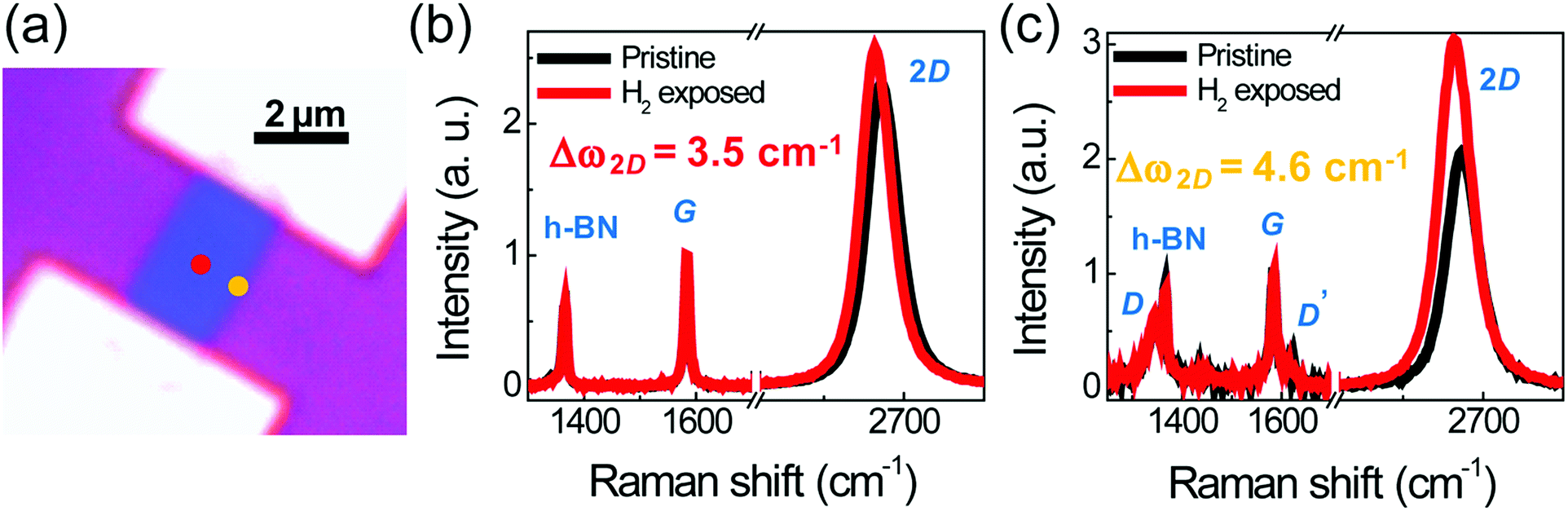 | ||
| Fig. 2 (a) Optical image of encapsulated edge-contact device where red and orange dot indicate measurement position of Raman spectroscopy. Raman spectra of h-BN/SLG/h-BN in the region of (b) center and (c) edge, respectively. Black and red curves are pristine and hydrogen treated, respectively. | ||
Fig. 3 shows the results of an electrical analysis of the hydrogenation of the h-BN/SLG/h-BN heterostructure. The edge-contact device shows typical transfer characteristics (R vs. Vg), as shown in Fig. 3(a). The transfer curve moved to negative gate voltage (Vg) side, indicating an electron doping effect. We undertook fitting to the transfer curve model of SLG,17 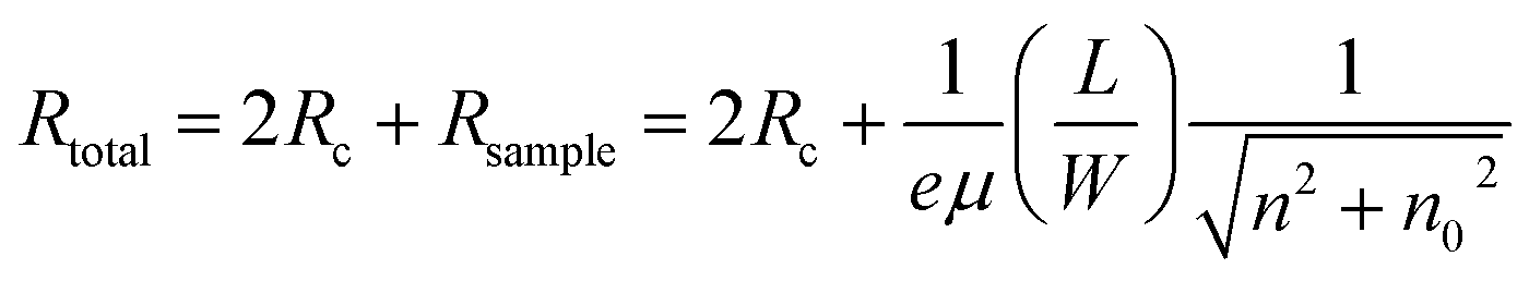 , where Rc, e, μ, L (W), n and n0 are the contact resistance, the charge element, the mobility, the length (width) of the sample, the carrier density and the residual carrier density, respectively. We used the carrier density relationship with a parallel conductor model, n = α(Vg − VD), where VD corresponds to the Dirac point and αSiO2(285 nm) = 7.5 × 1010 cm−2 V−1. It should be noted that the fittings were performed in the electron branch owing to the high asymmetry in the hole branch. The asymmetry is in agreement with the two-terminal graphene edge contact with lower work function metal, Cr electrode.6
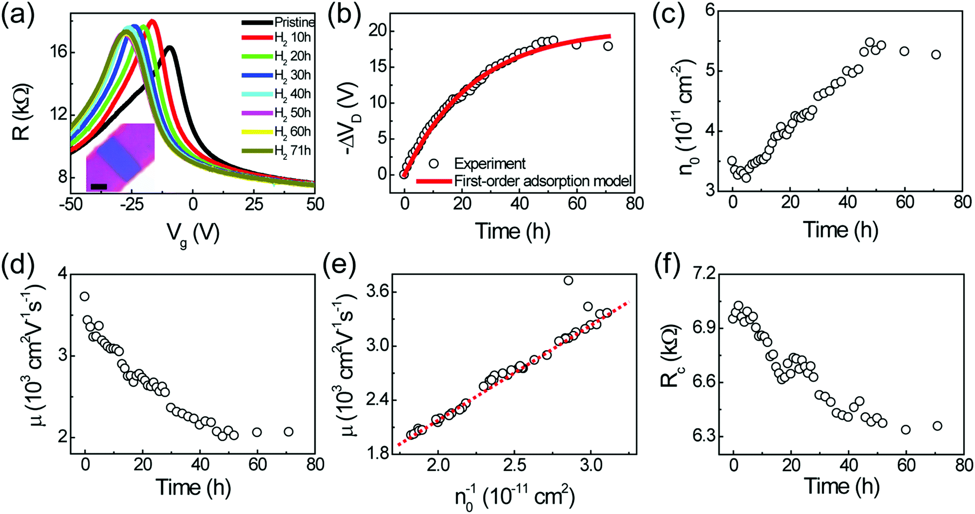 | ||
| Fig. 3 In situ electrical monitoring of h-BN/SLG/h-BN device. (a) Transfer characteristics (R vs. Vg) with hydrogen adsorption time. Inset is optical image of the device where scale bar is 2 μm. (b–d) Temporal evolution of −ΔVD, n0, and μ, respectively. (e) μ vs. n0−1 plot where red dashed line is guide for eye. (f) Temporal evolution of Rc. | ||
In Fig. 3(b), the temporal evolution of −ΔVD shows the first-order Langmuir type adsorption process, for which −ΔVD = −ΔVSatD (1 − e−kt), where −ΔVSatD and k denote the saturated VD and the kinetic coefficient, respectively. The experimental data (black circles) and the fitting function (red curve) yield the fitting parameters −ΔVSatD = 20 V and k = 0.04 h−1, respectively. This type of first-order adsorption has been observed in different cases of molecule adsorption in graphene-based systems.11,18,19 The fitting parameters are very close to previous results11 in which Bernal stacked bilayer graphene (BLG) on h-BN was exposed to hydrogen at both the surface and edge regions. This similar adsorption tendency indicates that hydrogen is adsorbed on the surface of h-BN/SLG/h-BN, which is consistent with the Raman spectroscopy results.
Fig. 3(c) and (d) indicate the temporal evolution of the residual density (n0) and the mobility (μ), respectively. As hydrogen is adsorbed, n0 increases and μ decreases due to the formation of C–H bonding. We also observed competitive behavior between n0 and the μ (Fig. 3(c) and (d)) and short-range scattering behavior (μ ∝ n0−1) (Fig. 3(e)), as shown in a previous report.11
The edge-contact device provides an ideal contact configuration of 2D materials. Wang et al. reported a novel one-dimensional contact geometry, leading to ideal contact performance and effect of chemical termination.6 The authors argued that the low contact resistance stems from the shorter bonding distance with larger orbital overlap in the edge-contact geometry. Furthermore, it has been discussed that oxygen termination can improve the contact performance. Note that our Rc is relatively high (∼7 kΩ for pristine) compared to that of devices in a previous study,6 even when using an identical metal electrode (Cr/Au). This may originate from unintentional fluorine termination during the O2/CF4 plasma etching process.20 We focus on the temporal evolution of Rc, which resembles the behavior of −ΔVD. In contrast to the Cr–H–graphene edge-contact configuration,20 Rc was reduced due to hydrogen adsorption (Fig. 3(f)). The absence of a metal electrode effect was previously discussed with the thermoelectric power (TEP) measurements in our previous report.21 The reduction of Rc can be understood by the variation of density of state after hydrogen adsorption. With electron doping, the density of state in graphene increases, yielding a lower value of Rc. Recently, a similar result using poly(4-vinylphenol)/poly(melamine-co-formaldehyde) (PVP/PMF) was reported22 in which the authors observed a reduction of Rc with the concentration of PVP/PMF. In this regard, even though the direct observation of atomic termination is necessary for future work, we may conclude that the reduction of Rc is from the doping of graphene sheet but not from the chemical termination between Cr and graphene edge. Since the temporal evolution of Rc was provided by in situ monitoring, fine manipulation of Rc could be achieved during hydrogen adsorption.
Finally, we confirmed the stability of C–H bonding by evacuating down to 6 × 10⁻⁶ Torr, as shown in Fig. 4. The transfer curves for high-pressure H2 (11 bar), low-pressure H2 (1 bar), and a vacuum (6 × 10⁻⁶ Torr) condition did not show any distinctive changes, indicating strong binding of the C–H bonds. Due to the strong binding, dissociative induced hydrogen adsorption can provide a means of stable chemical functionalization.
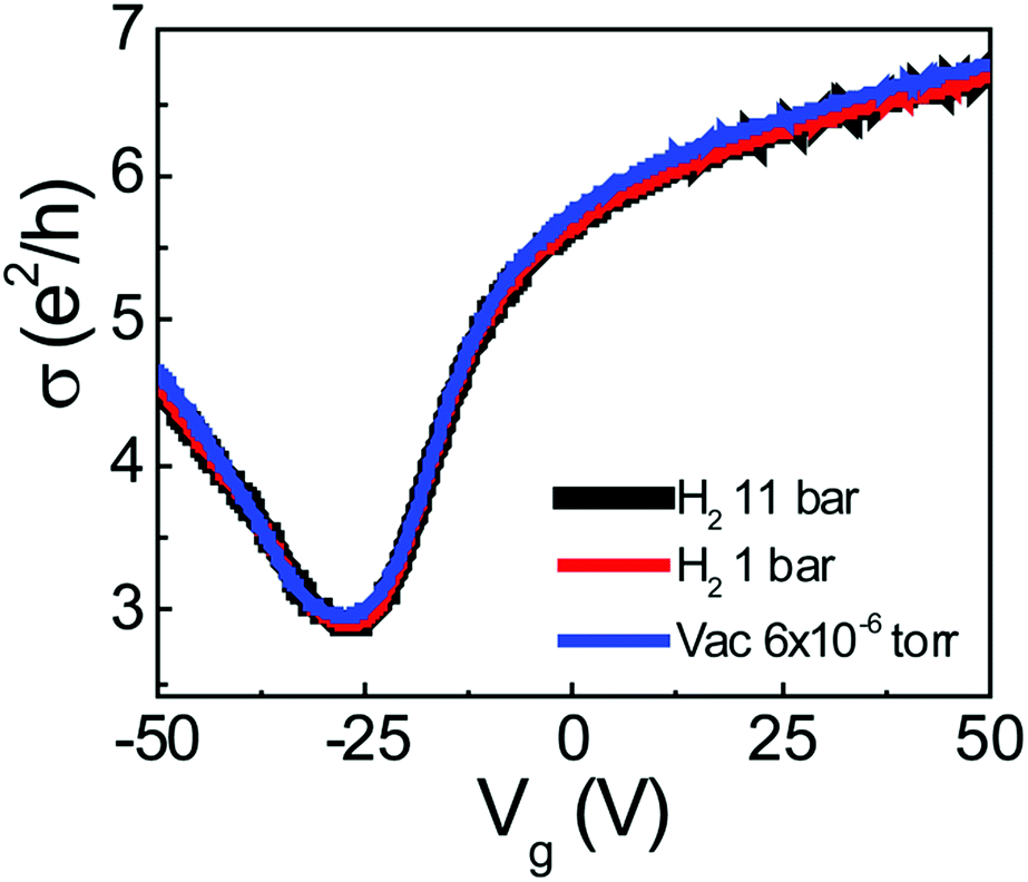 | ||
| Fig. 4 Transfer characteristics (R vs. Vg) with 11 bar, 1 bar of H2 gas molecules, and vacuum (6 × 10⁻⁶ Torr). | ||
4. Conclusions
In summary, we studied hydrogenation in the vdW heterostructure, which provides an encapsulated type of edge-contact geometry for CVD-grown SLG. Raman spectroscopy and electrical measurements showed the intercalation and adsorption of dissociated hydrogen. The in situ monitoring of the electrical properties revealed first-order adsorption, electron doping, short-range scattering, and reduced contact resistance. The electrical modulation is in good agreement with previous results with an ordinary device configuration. Specifically, considering the contact edge configuration, it was found that hydrogenation intrinsically affects graphene sheets rather than the atomic contact termination. Furthermore, strong C–H binding even under a high vacuum provides evidence of the stability of the hydrogenation process. The chemical manipulation of an encapsulated edge-contact device with the vdW heterostructure will contribute to the realization of high-quality 2D material-based electronic devices.Acknowledgements
This work was supported by the Swedish-Korean Basic Research Cooperative Program (No. 2014R1A2A1A12067266) of the NRF and by the FPRD of BK21 plus through the MEST, Korea. Partial support was provided by Leading Foreign Research Institute Recruitment Program through the National Research Foundation of Korea (NRF) funded by the Ministry of Science, ICT & Future Planning (2015K1A4A3047345). M. L. and D. H. J. acknowledge the support of the Pioneer Research Center Program through the NRF of Korea, funded by the Ministry of Science, ICT & Future Planning (No. 2013-006163). S. W. L. acknowledges the support from National Research Foundation of Korea (NRF-2015R1A2A2A05050829). B. H. K. acknowledges the support from the National Research Foundation of Korea (No. NRF-2014R1A1A1002467).Notes and references
- A. K. Geim and I. V. Grigorieva, Nature, 2013, 499, 419 CrossRef CAS PubMed.
- C. R. Dean, A. F. Young, I. Meric, C. Lee, L. Wang, S. Sorgenfrei, K. Watanabe, T. Taniguchi, P. Kim, K. L. Shepard and J. Hone, Nat. Nanotechnol., 2010, 5, 722 CrossRef CAS PubMed.
- L. Wang, Z. Chen, C. R. Dean, T. Taniguchi, K. Watanabe, L. E. Brus and J. Hone, ACS Nano, 2012, 6, 9314 CrossRef CAS PubMed.
- C. Melios, A. Centeno, A. Zurutuza, V. Panchal, C. E. Giusca, S. Spencer, S. R. P. Silva and O. Kazakova, Carbon, 2016, 103, 273 CrossRef CAS.
- A. Avsar, I. J. Vera-Marun, J. Y. Tan, K. Watanabe, T. Taniguchi, A. H. Castro Neto and B. Özyilmaz, ACS Nano, 2015, 9, 4138 CrossRef CAS PubMed.
- L. Wang, I. Meric, P. Y. Huang, Q. Gao, Y. Gao, H. Tran, T. Taniguchi, K. Watanabe, L. M. Campos, D. A. Muller, J. Guo, P. Kim, J. Hone, K. L. Shepard and C. R. Dean, Science, 2013, 342, 614 CrossRef CAS PubMed.
- D. C. Elias, R. R. Nair, T. M. G. Mohiuddin, S. V. Morozov, P. Blake, M. P. Halsall, A. C. Ferrari, D. W. Boukhvalov, M. I. Katsnelson, A. K. Geim and K. S. Novoselov, Science, 2009, 323, 610 CrossRef CAS PubMed.
- J. Katoch, J. H. Chen, R. Tsuchikawa, C. W. Smith, E. R. Mucciolo and M. Ishigami, Phys. Rev. B: Condens. Matter Mater. Phys., 2010, 82, 081417 CrossRef.
- B. H. Kim, S. J. Hong, S. J. Baek, H. Y. Jeong, N. Park, M. Lee, S. W. Lee, M. Park, S. W. Chu, H. S. Shin, J. Lim, J. C. Lee, Y. Jun and Y. W. Park, Sci. Rep., 2012, 2, 690 Search PubMed.
- H. González-Herrero, J. M. Gómez-Rodríguez, P. Mallet, M. Moaied, J. José Palacios, C. Salgado, M. M. Ugeda, J.-Y. Veuillen, F. Yndurain and I. Brihuega, Science, 2016, 352, 437 CrossRef PubMed.
- S. J. Hong, H. Kang, M. Park, M. Lee, D. Soler-Delgado, D. H. Jeong, Y. W. Park and B. H. Kim, RSC Adv., 2015, 5, 103276 RSC.
- J. Kim, C. H. Kwak, W. Jung, Y. S. Huh and B. H. Kim, Phys. Chem. Chem. Phys., 2016, 18, 15514 RSC.
- G. H. Han, J. A. Rodríguez-Manzo, C.-W. Lee, N. J. Kybert, M. B. Lerner, Z. J. Qi, E. N. Dattoli, A. M. Rappe, M. Drndic and A. T. C. Johnson, ACS Nano, 2013, 7, 10129 CrossRef CAS PubMed.
- L. Gao, W. Ren, H. Xu, L. Jin, Z. Wang, T. Ma, L. P. Ma, Z. Zhang, Q. Fu, L.-M. Peng, X. Bao and H.-M. Cheng, Nat. Commun., 2012, 3, 699 CrossRef PubMed.
- A. Das, S. Pisana, B. Chakraborty, S. Piscanec, S. K. Saha, U. V. Waghmare, K. S. Novoselov, H. R. Krishnamurthy, A. K. Geim, A. C. Ferrari and A. K. Sood, Nat. Nanotechnol., 2008, 3, 210 CrossRef CAS PubMed.
- Z. Chen, P. Darancet, L. Wang, A. C. Crowther, Y. Gao, C. R. Dean, T. Taniguchi, K. Watanabe, J. Hone, C. A. Marianetti and L. E. Brus, ACS Nano, 2014, 8, 2943 CrossRef CAS PubMed.
- S. Kim, J. Nah, I. Jo, D. Shahrjerdi, L. Colombo, Z. Yao, E. Tutuc and S. K. Banerjee, Appl. Phys. Lett., 2009, 94, 062107 CrossRef.
- S. Chen, W. Cai, D. Chen, Y. Ren, X. Li, Y. Zhu, J. Kang and R. S. Ruoff, New J. Phys., 2010, 12, 125011 CrossRef.
- I. Silvestre, E. A. de Morais, A. O. Melo, L. C. Campos, A.-M. B. Goncalves, A. R. Cadore, A. S. Ferlauto, H. Chacham, M. S. C. Mazzoni and R. G. Lacerda, ACS Nano, 2013, 7, 6597 CrossRef CAS PubMed.
- Q. Gao and J. Guo, APL Mater., 2014, 2, 056105 CrossRef.
- S. J. Hong, M. Park, H. Kang, M. Lee, D. Soler-Delgado, D. S. Shin, K. H. Kim, S. Kubatkin, D. H. Jeong, Y. W. Park and B. H. Kim, Appl. Phys. Lett., 2015, 106, 142110 CrossRef.
- H.-Y. Park, W.-S. Jung, D.-H. Kang, J. Jeon, G. Yoo, Y. Park, J. Lee, Y. H. Jang, J. Lee, S. Park, H.-Y. Yu, B. Shin, S. Lee and J.-H. Park, Adv. Mater., 2016, 28, 864 CrossRef CAS PubMed.
Footnote |
| † Present address: Institut für Festkörperphysik, Leibniz Universität Hannover, Appelstraße 2, 30167, Hannover, Germany. |
| This journal is © The Royal Society of Chemistry 2017 |