
 Open Access Article
 This Open Access Article is licensed under a Creative Commons Attribution-Non Commercial 3.0 Unported Licence
Photonic sintering of a ZnO nanosheet photoanode using flash white light combined with deep UV irradiation for dye-sensitized solar cells†
Supriya A. Patil ab,
Hyun-Jun Hwanga,
Myeong-Hyeon Yua,
Nabeen K. Shresthac and
Hak-Sung Kim*ab
ab,
Hyun-Jun Hwanga,
Myeong-Hyeon Yua,
Nabeen K. Shresthac and
Hak-Sung Kim*ab
aDepartment of Mechanical Engineering, Hanyang University, Haengdang-dong, Seongdong-gu, Seoul 133-791, South Korea. E-mail: kima@hanyang.ac.kr
bInstitute of Nano Science and Technology, Hanyang University, Seoul, 133-79, Korea
cInstitute of Materials Design, Department of Chemistry, Hanyang University, Seongdong-gu, 133-791 Seoul, Repulic of korea
First published on 20th January 2017
Abstract
The present report details research work on the photonic sintering of ZnO nanosheets (ZnO NSs), which were synthesized via a solid-state synthesis method. The sintering was performed using flash white light (FWL) combined with deep UV irradiation (photonic sintering) under ambient conditions at ultra-high speed, which is a superior process over the conventional thermal-sintering process. Furthermore, the application of this method was demonstrated in dye-sensitized-solar cells (DSSCs), where a power conversion efficiency (PCE) of 2.9% was achieved when the photoanode was annealed using photonic sintering with a FWL of 20 J cm−2 combined with deep UV irradiation of 30 mW cm−2 irradiation power. This PCE is higher than that of the pristine ZnO NSs (PCE = 1.5%) and of the thermally sintered ZnO NS photoanode (PCE = 2.0%). The superior performance of the dye cell with the photonic-sintered ZnO NSs is attributed to the better interconnection, higher effective electron diffusion coefficient (Dn), higher electron diffusion length (Ln) and a higher amount of dye loading than that of the pristine ZnO NS photoanode. The improved PCE suggests that the photonic-sintering method, as well as being extremely simple, is highly effective and enables a fast annealing for photoanodes in DSSCs and could be particularly beneficial for low-temperature-based solar cells.
Introduction
Dye-sensitized solar cells (DSSCs) have emerged as a potential alternative to silicon-based solar cells. So far, a PCE of over 13% have been reported for DSSCs as a result of continuous efforts made in the optimization of photoanodes, sensitizers, electrolytes and counter electrodes.1 Apart from the widely used TiO2 photoanodes, other metal oxides, such as ZnO, SnO2 and Zn2SnO4, have received much attention.2 Among these, the use of ZnO as an alternative metal oxide in DSSCs offers several advantages, such as high electron mobility (205–300 V−1 s−1), a wide band gap (3.37 eV) and a large excitation binding energy (60 MeV) at room temperature.3,4 Zinc oxide has a much higher electron diffusivity than TiO2, and furthermore, it is much easier to crystallize and grow into various structural forms, such as zero-dimensional (0D) to three-dimensional (3D). Among these, ZnO composed of nanosheets (ZnO NSs) have exhibited superior optical and electrical performances. Compared to ZnO nanocrystal aggregates, ZnO NS-based nanostructures are more advantageous in electron transport5,6 and also, due to their diverse morphologies, they are considered more promising than the other metal oxides in the fields of photocatalysts,7,8 gas sensors,9 optoelectronics and so on. Therefore, it is desirable to study the special structures of ZnO NSs in terms of their potential in photoelectrochemical device applications.However, the highest reported PCE achieved so far for ZnO-based DSSCs is 6.58%,10 which is much lower than that achieved by TiO2-based DSSCs (11.5%).1,11 This limited performance of ZnO is due to the poor chemical stability of ZnO in acidic dye (the formation of Zn+/dye), which can block the injection of electrons from the dye to the semiconductor.12,13 To improve the PCE of ZnO-based DSSCs, several strategies are being studied, such as designing new dyes that are suitable for ZnO, developing new ZnO photoanodes with novel morphologies and developing different sintering processes.
To date, ZnO photoanodes have been synthesized through the following approaches: hydrothermal,5,14 chemical bath deposition (CBD),6,15 electrodeposition,16 direct precipitation,17 sol–gel method,18 physical or chemical vapour deposition,19 solid-state synthesis4 and so on.20 Among these, solid-state synthesis is the simplest approach to synthesize ZnO NSs. In the present study, ZnO NSs were prepared using our previously reported method.4
Traditionally, thermal sintering (at a high temperature of 250–500 °C) methods have been used to increase the crystallinity of TiO2,21 SnO2,22 and ZnO23 photoanodes, reduce the grain boundary between nanoparticles and to remove surface contamination. Consequently, an enhanced PCE has been achieved. However, the high-temperature process has some limitations, and the process is not compatible with flexible devices, in which generally polyethylene terephthalate (PET) or polyethylene naphthalate (PEN) are used as the substrate. Although a photoanode based on a heat-sensitive substrate can be sintered at low temperature, the low-temperature sintering process requires a long heating time; for instance, at least few tenths of minutes to hours. Nevertheless, in contrast to high-temperature thermal sintering, low-temperature sintering results in a lower PCE of the device. Considering these limitations of the conventional sintering process, the development of a novel sintering technique that is suitable for all types of solar cells is highly desired but it is still challenging to achieve a better PCE swiftly and efficiently without damaging the nanostructures and heat-sensitive substrates.24
In recent years, several researchers have demonstrated that flash white light (FWL),25–30 UV irradiation,31 microwave irradiation,32 laser sintering33–35 and IR sintering36 can be used for sintering a metal oxide and Cu-nanolinks and for the fabrication of TiO2 as well as for counter electrode development. Among these, FWL-based sintering is essentially a sintering technique, which, in contrast to conventional oven sintering, employs the heat generated locally by the absorption of visible light in the target material to achieve the necessary temperature for sintering the material. The most commonly used light source for FWL sintering is a xenon stroboscope lamp, which emits radiation in the range between 200 and 1200 nm, which, hence, covers the entire visible spectrum. In fact, sintering is a much more energy efficient technology.37 In particular, a combination of specifically shaped reflectors allows high energy densities and, thus, locally high temperatures to be achieved without requiring an enormously strong power supply.38 One of the key advantage of FWL sintering is that it can reduce the risk of thermal damage to the heat-sensitive organic materials used in optoelectronic devices, such as organic semiconductors and heat-sensitive substrates. Recently, Lee et al. utilized organic buffer layer annealing via FWL in organic photovoltaic (OPV) devices.39 Using UV irradiation, Miyasaka et al. proposed a paste composed of nanocrystalline particles and utilizing TiOX sol–gel with the function of acting as a binding agent.40 Arakawa et al. developed a water-based binder-free paste of TiO2. UV irradiation has been used as a post-processing step to remove impurities and binder from a titania film for DSSCs.41
Considering these advantages, and to address the existing challenge of minimizing sintering problems associated with photoanodes in DSSCs, we studied photonic sintering (FWL combined with deep UV) in ZnO-based DSSC applications.
For the first time, we used FWL combined with deep UV as a photonic-sintering source for ZnO photoanodes in DSSC applications which represents an alternative to the previous reports that predominantly used deep UV irradiation.42–46
Experimental
Chemicals
All the reagents used in the present work were of analytical grade. Zinc nitrate [Zn(NO3)2·6H2O], 98%, (Deaejung Chemicals, S. Korea) and sodium hydroxide (NaOH, 97%, Kanto Chemicals, Japan) were used as received without further purification. Triple-distilled water was used throughout the experiments. N719 dye was obtained from Solaronix SA (Switzerland). Iodide/triiodide (I−/I3−)-based liquid-electrolytes were used for the DSSCs.Synthesis
The ZnO NSs were synthesized via a solid-state reaction between two commonly available and low-cost reactants, namely Zn(NO3)2 and NaOH. In a typical solid-state synthesis, 10 g powder of zinc precursor and 5 g NaOH (2![[thin space (1/6-em)]](https://www.rsc.org/images/entities/char_2009.gif) :1 w/w) were mixed together into a glass vial without adding any solvent, and the mixture was then stirred using a magnetic stir bar for 5–10 min. After completion of the reaction, a thick slurry paste was obtained. The products were washed by dispersing them in water and then separating them using centrifugation. The washing step was repeated three times. Finally, without drying, the obtained ZnO NS nanostructures were dispersed again in 15 ml of deionized water and 5 ml of ethanol (3:1 v/v) to prepare a homogeneous paste for the fabrication of thin films using a doctor blade method.4
:1 w/w) were mixed together into a glass vial without adding any solvent, and the mixture was then stirred using a magnetic stir bar for 5–10 min. After completion of the reaction, a thick slurry paste was obtained. The products were washed by dispersing them in water and then separating them using centrifugation. The washing step was repeated three times. Finally, without drying, the obtained ZnO NS nanostructures were dispersed again in 15 ml of deionized water and 5 ml of ethanol (3:1 v/v) to prepare a homogeneous paste for the fabrication of thin films using a doctor blade method.4
The reactions involved in the formation of the zinc oxide are given below:
| Zn(NO3)2 + 2NaOH → Zn(OH)2 + 2Na(NO3), | (1) |
| Zn(OH)2 → ZnO + H2O. | (2) |
The prepared ZnO NS pastes were printed onto FTO-coated glass substrates using the doctor blade method.
Photonic sintering of the ZnO NSs
The above-synthesized ZnO NSs were sintered via FWL combined with deep UV under ambient conditions (Scheme 1). The FWL set-up consisted of a xenon flash lamp (PERKIN ELMER Co; UK), a power supply, capacitors, a simmer triggering controller, a pulse controller (PSTEK Co; Korea) and a water cooling system. White light from a xenon flash lamp has a broad wavelength range from 380 to 950 nm. A commercial deep UV system (100 Mw, LUMATEC SUV-DC) with a wavelength range of 180 to 280 nm was used in this study. The irradiation energy density (J cm−2) of the FWL and the power of the deep UV irradiation (mW cm−2) were varied to optimize the photonic-sintering conditions so as to achieve the best ZnO NS-based photoanode. | ||
| Scheme 1 (a) Figures showing the physical principles involved in the FWL sintering of ZnO NSs on a FTO substrate. (b) Schematic for the sintering of ZnO NSs using FWL combined with deep UV: (i) ZnO NSs without FWL (W/O), (ii) ZnO NSs with FWL sintering, (iii) ZnO NSs with FWL and deep UV (FWL + UV) sintering, and (iv) ZnO NSs sensitized with N 719 dye. Schematic presentation of the DSSCs' FTO/ZnO NS/N 719 dye/electrolyte (iodide/triiodide)/Pt structure is shown in (c). | ||
Thermal sintering of the ZnO NSs
For the thermal sintering of the ZnO NS photoanodes, we used a programmable hot plate. The ZnO NS photoanode was placed in direct contact with the plate surface at 250 °C for 30 min.DSSCs fabrication
Fluorine-doped tin oxide (FTO) glass substrates were first cleaned in detergent water, acetone and isopropyl alcohol for 10 min each using an ultrasonic bath. The substrates were then dried in a stream of argon and stored for further use. The doctor blade technique was used to fabricate binder-free ZnO NS photoanodes. After drying in air, the photoanode films were sintered using FWL with and without a combination of deep UV light at various pulse numbers and irradiation energies. After sintering, the films were sensitized with 0.5 mM N719 prepared in a mixture solution of absolute ethanol:acetonitrile (1:1 v/v) for 60 min.46
Characterizations
The crystal structures and phases of the ZnO NSs before and after sintering were confirmed using X-ray diffraction (XRD) patterns obtained using an X-ray diffractometer (Rigaku D/MAX 2500 V, Cu-Kα, λ = 0.15418 nm). The morphology of the ZnO NS films was monitored using SEM (HitachiS-4200). The XPS measurements were performed using ESCALAB220i on the sample with an Al α X-ray source. In order to measure the solar-to-electric power conversion efficiency, the electrodes were incorporated into thin layer sandwich-type cells with a Pt-coated FTO as the counter electrode separated by the iodide/triiodide (I−/I3−)-based liquid-electrolyte in a sandwich-type arrangement using polyimide tape (having a thickness of ∼0.03 mm), which also served as a spacer for the cell. The cell performance was measured via the irradiation of 100 mW cm2 white light (1 sun, 1.5 AM) using a solar simulator (PCE-L01, Peccell). The current density was measured using a Keithley 2400 source meter by defining an area of 0.25 cm2 of the photoanode. Electrochemical impedance spectra (EIS) were obtained using an Ivium CompactStat impedance analyzer in the range of 0.01 Hz to 1.5 MHz. All the spectra were recorded under open circuit conditions under 1 sun illumination. The data was fitted using the Z-view software.Result and discussion
In this section, we describe the development and optimization of photonic sintering of the ZnO NSs on the FTO substrate and analyze the performance of the ensuing DSSCs. Scheme 1a shows the physical principles involved in the FWL sintering of ZnO NSs on a FTO substrate. The FWL sintering process is described based on the emission spectrum of the lamp and the known wavelength dependencies of the optical properties of the ZnO materials, using e.g. Beer–Lambert law; wherein, the absorbed part of the radiation is subsequently dissipated as heat at the location of absorption. For highly absorptive materials, the heat generation by radiation can be described as occurring at the surface. Under this condition, some amount of heat is re-emitted from the surface following Stefan–Boltzman's law, and another part is conducted into the bulk of the materials.47–49 Photonic sintering has some key effects that ultimately lead to good cell performance: (i) better interconnection, (ii) high mobility and (iii) the amount of dye loading, which is explained in a later section. Scheme 1b shows the designed ZnO NS photoanodes for the photonic-sintering process. Briefly, these comprise: (i) ZnO NSs without FWL (W/O), (ii) ZnO NSs with FWL sintering, (iii) ZnO NSs with FWL combined with deep UV (FWL + UV) sintering, and finally sensitizing all of these (iv) ZnO NSs with N 719 dye.The basic structure of the cell has four primary parts. The conducting glass with a coating of semiconductor ZnO film is deposited on the conducting side and then immersed in a mixture of organic N 719 dye. After saturating the film in the dye solution, a thin layer of dye is left on the surfaces of the ZnO NSs. Later on, a thin layer of iodide electrolyte is spread over a conductive sheet using polyimide as a separate support made with a thin layer, using platinum as a counter electrode. The front and back parts are then joined and closed together to prevent the electrolyte from leakage. A schematic diagram of a DSSC assembly is shown in Scheme 1c.
Subsequently, the ZnO NS films were irradiated with FWL using pulse energy from 15 to 35 J cm−2 (using a single pulse with a pulse duration of 20 ms), with the experimental details given in the ESI, see also Fig. S1a.† SEM images of the ZnO W/O FWL and the FWL-sintered ZnO NS films with different irradiation energies are shown in Fig. 1a–f. From the SEM, it is evident that the assembly of ZnO NSs with an average diameter of 40 to 90 nm constituted the film. The top surface view of the FWL-sintered ZnO NS films revealed a macroporous structure, indicating that no significant morphologies difference were observed.
 | ||
| Fig. 1 Scanning electron microscope images (false color) of the ZnO NS films: (a) ZnO NS W/O FWL (pristine), (b)–(f) FWL sintered at 15 J cm−2, 20 J cm−2, 25 J cm−2, 30 J cm−2, and 35 J cm−2, respectively. | ||
Furthermore, the pristine and FWL-sintered ZnO NS films were used as a photoanode in DSSCs. Initially, the FWL pulse energy varied from 15 to 35 J cm−2 and the initial current–voltage (J–V) curves were measured. It was found that the PCE (η) of the ZnO NS-based DSSCs increased 2.5%, which is higher than that of pristine ZnO NS (η = 1.5%) when a FWL irradiation energy of 20 J cm−2 was employed (ESI, Fig. S4†). Later on, this decreased when the FWL energy was increased from the 25 to 35 J cm−2. The ZnO photoanode sintered with FWL energy showed a low efficiency, which could be due to damage of the ZnO NSs by the use of excessive FWL energy, suggesting that this irradiation energy range is not favourable for the light-harvesting ability of the dye. Due to this, the nanoparticles in the NS become larger, leading to a decreased surface area of the photoanode and subsequently a decreased dye loading amount. For this reason, the sintering power for the ZnO NS photoanode was selected to be 20 J cm−2 for the further experiments. Comparative J–V plots of the pristine and FWL-sintered ZnO NSs and the detailed photovoltaic parameters were extracted from Fig. 2, and are summarized in the ESI, Table S1.†
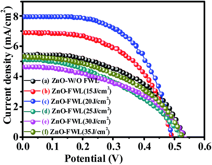 | ||
| Fig. 2 J–V curves of DSSCs consisting of ZnO NSs without (W/O) FWL sintering (a), FWL sintered at (b) 15 J cm−2 energy, (c) 20 J cm−2, (d) 25 J cm−2, (e) 30 J cm−2, and (f) 35 J cm−2. | ||
To further improve the PCE of the FWL-sintered ZnO NS photoanodes and to study the influence of UV light on the ZnO photoanode, FWL irradiation was combined with deep UV. The power of the deep UV irradiation varied from 0.75 to 30 mW cm−2, maintaining all the other conditions at their optimum (ESI, Fig. S1b†). For the sake of comparison, the ZnO NSs were thermally treated at 250 °C with the same batch. The surface of the ZnO photoanodes sintered with various sintering sources were observed via optical microscopy images (OM) (ESI, Fig. S2†). The surface of the ZnO NS photoanode film clearly showed the effect of FWL and photonic sintering throughout the film. For example, the ZnO NS W/O FWL (Fig. S2a†) did not show any structural defect on the surface, whereas small black spots were observed with the ZnO NSs prepared by sintering with FWL, which were evidence of well-photonic-sintered ZnO NS films (ESI, Fig. S2(b–e)†). These black spots could be the result of the removal of unwanted residues during sintering. In addition, these spots could be also formed due to the direct contact and fusion of adjacent ZnO NSs during sintering.50,51
Fig. 3a–c shows the SEM images of ZnO W/O FWL (a), thermal sintering at 250 °C (b), and ZnO with FWL (c). The (d–f) images show the photonic sintering with various UV powers. It can be seen that the surfaces of all the samples have become rough and present crystallite grains of varying shapes in the nanometre scale. These crystallites are randomly distributed and irregularly disoriented. It was noted that the sintering of ZnO NSs using photonic-sintering FWL + UV energy helped to grow larger grains of oxide particles, reducing the grain boundary clearly, as shown in Fig. 3f.
 | ||
| Fig. 3 Scanning electron microscope images (false color) of the ZnO NS films, (a) ZnO W/O FWL, (b) ZnO-250 °C, (c) ZnO-FWL (20 J cm−2), and (d)–(f) photonic-sintering ZnO-FWL + UV (0.75 mW cm−2), ZnO-FWL + UV (1.5 mW cm−2), and photonic-sintering ZnO-FWL + UV (30 mW cm−2), respectively. SEM images (g)–(l) show the cross-sectional views for the corresponding ZnO NSs. | ||
The increase in particle size and the reduced grain boundary regions affect the solar cell efficiency in two different ways. On the one hand, the surface of the semiconductor is reduced with the increased grain growth, leading to lower dye adsorption, which thereby lowers the light-harvesting efficiency. On the other hand, reducing the grain boundaries decreases the dangling bonds that act as charge-trapping centres, which thereby improves the charge-collection efficiency of the photoanode. Hence, optimization of the grain growth and reduction in the number of charge-trapping centres are required to improve device efficiency. This can be achieved by increasing the sintering power, which leads to conglomeration of the smaller grains and them fusing together into ZnO NSs in the photonic-sintered photoanodes. Thus, compared to the pristine sample, a significant difference in the morphology was observed.
Fig. 3g–l show cross-sectional images of the ZnO NS films without sintering, with thermal sintering, with FWL (20 J cm−2) and with FWL + UV sintering, respectively. The thickness of the pristine ZnO NS film was about 28.7 μm (Fig. 3g). However, after sintering, the ZnO NS film shrunk to some extent. Importantly, DSSCs consisting of ZnO NS-structured thin films sintered at a higher photonic energy (FWL 20 J cm−2 + UV 30 mW cm−2) have a higher PCE. The improved photovoltaic performance with increasing the photonic energy is due to the fact that photonic sintering leads to the conversion of the ZnO NS photoanode film into a highly crystalline structure. This reduces the charger trapping centres, improves the network structure of the ZnO NS photoanode and improves the interconnection, thereby resulting in a swift diffusion of the electrolyte and good charge transportation.52,53
Fig. 4 presents the XRD pattern of the ZnO NSs grown on a glass substrate. All of the peaks in the obtained spectrum are well indexed with the hexagonal phase of ZnO (JCPDS card no 36-1452),54 indicating that the ZnO NS structures were crystallized in a typical wurtzite structure. A small shift to lower diffraction angles of the diffraction patterns can be observed (ESI, Fig. S3a†), which is related to compressive stress caused by the sintering of the ZnO NSs. The crystalline sizes of the ZnO NSs were calculated using Scherrer's equation, given below:55
| D = 0.9λ/(βcosθ) |
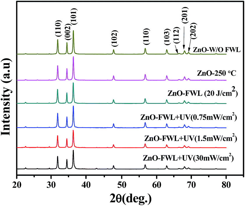 | ||
| Fig. 4 XRD patterns of ZnO NSs W/O sintering, with thermal sintering, with FWL and with photonic sintering. | ||
Additionally, the chemical states of the surface elements before and after photonic sintering the ZnO NS films were studied by X-ray photoelectron spectroscopy (XPS) analysis. The Zn 2p core level XPS spectra are presented in Fig. 5a. The Zn 2p spectra of the ZnO NS show two strong peaks centred at 1021.18 and 1044.28 eV, corresponding to Zn 2p3/2 and Zn 2p1/3, respectively, while those after the photonic sintering [FWL + UV (30 mW cm−1)2] were observed, respectively, at comparatively higher binding energies of 1021.38 and 1044.53 eV. These values are in good agreement with the binding energies of Zn+ ions. These binding energy values indicates that the ZnO NSs before and after sintering have different chemical sates despite them having the same morphology. Furthermore, ZnO NS W/O FWL shows an O 1s peak at 529.83 eV, which corresponds to the lattice O2− of ZnO. The peaks exhibit a small shift in the highest binding energy, centred at 530.03 eV, which is attributed to the adsorbed OH− (OH(ads)) located on the surface of the ZnO NSs.58
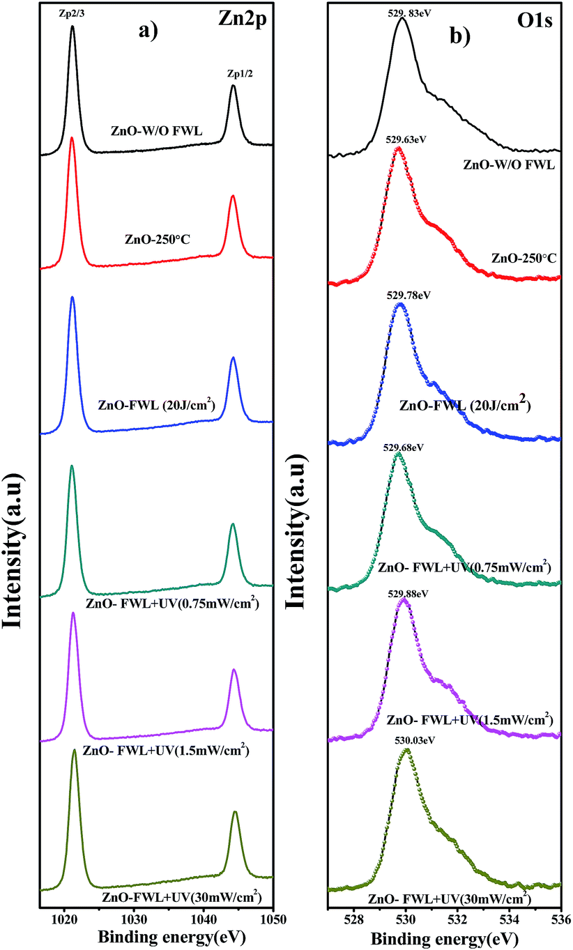 | ||
| Fig. 5 XPS spectrum of (a) Zn 2p, and (b) O 1s core level XPS spectra of ZnO NS W/O FWL, with thermal sintering, with FWL and with photonic sintering, respectively. | ||
The structural investigations before and after photonic sintering of the ZnO NSs were analysed by FTIR spectroscopy, as shown in Fig. S6.† The IR bands at ∼3392, ∼1500 and ∼495 cm−1 correspond to –OH stretching vibrations, C![[double bond, length as m-dash]](https://www.rsc.org/images/entities/char_e001.gif) O and Zn–O stretching vibrations of bulk ZnO, respectively, As compared to the ZnO NS W/O FWL, the OH-bonding hump in the FTIR spectrum of the FWL-sintered and photonic-sintered ZnO NS film is smaller, which can be clearly seen in Fig. S5.† The spectroscopic studies indirectly provide information about the surface character of the ZnO NSs.59
O and Zn–O stretching vibrations of bulk ZnO, respectively, As compared to the ZnO NS W/O FWL, the OH-bonding hump in the FTIR spectrum of the FWL-sintered and photonic-sintered ZnO NS film is smaller, which can be clearly seen in Fig. S5.† The spectroscopic studies indirectly provide information about the surface character of the ZnO NSs.59
Fig. 6a shows the current–voltage (J–V) curves of W/O FWL, with FWL, thermal-sintered and photonic-sintered photoanodes. The detailed photovoltaic parameters were extracted from the J–V curves and are summarized in Table 1. As evident from Fig. 6a and Table 1, it can be assumed that the pristine and FWL-sintered ZnO NS photoanodes have a high density of surface states, causing a severe recombination of photogenerated electrons, which results in lower PCE values of 1.5% and 2.5%, respectively. On the contrary, the photonically sintered ZnO NS photoanodes show a reduced recombination of photogenerated electrons and exhibit an open circuit voltage (Voc) of ∼0.56 V, a short circuit current density (Jsc) of ∼7.5 mA cm−2, a fill factor (FF) of ∼0.67 and a power conversion efficiency (η) of ∼2.9%.
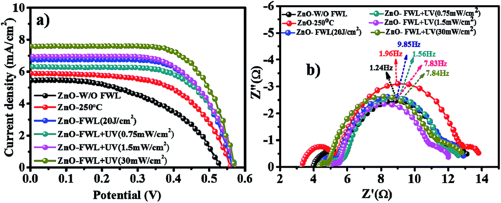 | ||
| Fig. 6 J–V curves of DSSCs consisting of ZnO NS photoanodes with and without photonic sintering (a). (b) Nyquist plots of DSSCs employing ZnO NSs with and without photonic sintering (inset in (b) is estimated from the characteristic frequencies of the impedance semicircle at middle frequencies, where the lifetime of electrons in the ZnO(τ) can be calculated according to the relation τ = (1/2πfmax), where fmax is the maximum frequency of the mid-frequency peak). | ||
| Sample name | Amount of dye loading (mol cm−2) | Voc (V) | Jsc (mA cm−2) | FF | PCE (η%) |
|---|---|---|---|---|---|
| ZnO W/O FWL | 1.12 × 10⁻⁷ | 0.55 | 5.4 | 0.50 | 1.5 |
| ZnO-250 °C | 1.35 × 10⁻⁷ | 0.55 | 5.9 | 0.59 | 2.0 |
| FWL (20 J cm−2) | 1.41 × 10⁻⁷ | 0.56 | 6.7 | 0.65 | 2.5 |
| ZnO-FWL + UV (0.75 mW cm−2) | 1.16 × 10⁻⁷ | 0.57 | 6.3 | 0.65 | 2.4 |
| ZnO-FWL + UV (1.5 mW cm−2) | 1.32 × 10⁻⁷ | 0.57 | 6.9 | 0.63 | 2.5 |
| ZnO-FWL + UV (30 mW cm−2) | 1.60 × 10⁻⁷ | 0.56 | 7.5 | 0.67 | 2.9 |
In this study, the devices after sintering demonstrated an improved FF from 0.50 to 0.67 (a 14% difference in the cells with the lowest and highest efficiency), and an enhanced Voc from 0.55 to 0.56 V. Owing to the conversion of ZnO NSs into bigger crystallites, the absorbed pulse energy during photonic sintering can effectively promote electrical contact between the ZnO NSs without damaging the substrate.
The enhanced PCE can be attributed to the conversion of ZnO NSs to a highly crystalline structure and the better interconnectivity as a result of the photonic sintering, which reduces the grain boundary defects, and thereby improves the charge transfer and recombination processes in DSSCs. Also, it can be explained by considering that the ZnO photoanode sintered at a photonic-sintering power of 20 J cm−2 + deep UV power of 30 mW cm−2 retains a higher light-harvesting ability, which improves the electron injection efficiency as a result of the observed enhancement of the photoconversion efficiency, compared to the thermally sintered ZnO NS-based device, with Jsc value of 5.9 mA cm−2 for thermal sintering vs. 7.5 mA cm−2 for photonic sintering and a PCE of 2.0% for thermal vs. 2.9% for photonic sintering. From Fig. S6,† the UV-vis absorption spectra of the photonic-sintered ZnO NSs show that the absorbance of the ZnO NSs is increased with increasing the photonic-sintering power from 0.75 to 30 mW cm−2, this trend is well supported to increase the efficiency and Jsc with a high light-harvesting efficiency.
In addition the amount of dye loading (1.60 × 10⁻⁷ mol cm−2) in the photonic-sintered ZnO under 30 mW cm−2 power was found to be higher than that in the photonic-sintered ZnO under 0.75 mW cm−2 power and photonic-sintered ZnO under 1.5 mW cm−2 power, respectively, and, as a result, high efficiency was observed in the case of photonic-sintered ZnO under 30 mW cm−2 power, with a Jsc of 7.5 mA cm−2 and a PCE of 2.9%.
A key question though can be raised: why does photonic sintering result in the observed changes in the photoelectrochemical and kinetic parameters of dye-sensitized solar cells? Based on our results demonstrated above, there are two key reasons. First, the photonic sintering might have resulted in cleaner ZnO NS surfaces due to the removal of some undesired residues, resulting in a slowdown of the interfacial recombination kinetics of the solar cell. Second, photonic sintering leads to the conversion of the ZnO NS photoanode film into a highly crystalline structure. This improves the interconnectivity between the ZnO NSs in the photoanode. This reduces the grain boundary defect sites and improves the network structure of the ZnO NS photoanode. Consequently, electron transfer resistance is decreased, thereby helping to establish more fluent electron transfer paths. In addition to these improvements, residual OH-bonds acting as charge-trapping centres can be reduced by applying UV radiation, and thereby the electron transfer resistance is further reduced.31,60,61
Table 2 shows a comparative study of various sintering methods and the resultant PCEs in DSSCs and in organic photovoltaic solar cells (OPVs). Compared to other low-temperature methods, the biggest advantage of this photonic-sintering method is that it can sinter the ZnO NSs in a few milliseconds in a large area without damage on the substrate. The photonic-sintering method can also sinter a large area as it can cover a large sintering area, depending on the xenon lamp size used. This research clearly shows that photonic sintering is a superior sintering method. The important advantage of photonic sintering is that it eliminates the need for heating at high temperature, which not only reduces the fabrication time, but also allows the use of inexpensive plastic substrates applicable in flexible electronics.62–65
| No | Sintering methods used | Minimum efficiency (η%) | Maximum efficiency (η%) | Increased efficiency (η%) | Reference |
|---|---|---|---|---|---|
| 1 | FWL (TiO2) | 1.63 | 1.85 | 0.22 | 26 |
| 2 | Microwave irradiation (TiO2) | 3.86 | 5.51 | 1.65 | 33 |
| 3 | UV laser-sintered (TiO2) | 4.8 | 5.2 | 0.40 | 34 |
| 4 | Laser-sintered (TiO2) | 0.71 | 1.84 | 1.13 | 36 |
| 5 | Near infrared (NIR) heating (TiO2) | 2.6 | 2.9 | 0.30 | 37 |
| 6 | Intense pulsed light (IPL)–organic photovoltaics (ZnO) | 2.0 | 2.4 | 0.40 | 40 |
| 7 | Photonic sintering (FWL + UV-ZnO) | 1.5 | 2.9 | 1.40 | Present work |
In order to show that our photonic-sintered ZnO NSs led to the improved charge transfer characteristics of the dye cell, we conducted electrochemical impedance spectroscopy (EIS) measurements. The equivalent circuit used for the EIS measurements and the extracted EIS electronic parameters are presented in the ESI in Fig. S7 and Table S2.†
The Nyquist plot is shown in Fig. 6b. For this, electrochemical impedance spectroscopy (EIS) was used and the EIS spectra were measured under illumination (100 mW cm−2, AM 1.5).
Generally, three typical frequency peaks are observed in the EIS spectra of DSSCs. The ohmic series resistance Rs corresponds to the electrolyte and electronic contact in the device. The small semicircle at high frequency results from the charge transfer resistance at the ZnO/FTO interface, R1. The large semicircle at low frequencies corresponds to the resistance at the ZnO NS photoanode-dye/I−/I3−electrolyte interface R2. The finite Warburg impedance-related elements associated with the diffusion process are Wo and these parameters are influenced by the nature of the porous electrode/electrolyte interface and the counter electrode/electrolyte. The symbol CPE describes the constant phase element of the capacitance, which represents a non-ideal frequency-dependent capacitance due to a non-uniform distribution of the current by the material heterogeneity. However, R1 and R2 are the main factors in the present study that influence directly the photovoltaic performance of the cell. Therefore, the discussion on the impedance measurements will be focused mainly on R1 and R2. The second semicircle, as shown in Fig. 6b, can be used to estimate the mean electron lifetime (τn) in the photoanode from the characteristic frequencies of the impedance semicircle at middle frequencies, according to the relation τn = (1/2πfmax), where fmax is the maximum frequency of the mid-frequency peak. The fitted Rs, R1 and R2 values for the ZnO NS photoanodes treated at various combinations of thermal, FWL and FWL with deep UV power are shown in the ESI (Table S2†). The Rs, R1 and R2 values for W/O FWL, thermal sintering and phonic sintering were estimated to be in the range of (Rs) 3.9, ∼5.02 and 4.3 Ω cm2, while the R1 value decreases from 1.48 to 0.55 Ω cm2 and R2 is in the range of 5.45–7.51 Ω cm2, as shown in detail in Table S2.† Such a decrease in resistance after photonic sintering is attributed to the high charge transportation rate with low recombination.66–68
The electron transport resistance in the ZnO NS photoanode, the charge transfer resistance of the charge recombination between electrons in the ZnO photoanode and I3− ions in the electrolyte and the chemical capacitance of the ZnO photoanode were the three parameter used to determine the parameters for the evaluation of cell performance, such as the electron life time (τn), electron transport time (τd), charge-collection efficiency (ηcc), diffusion length (Ln), diffusion coefficients (Dn) and electron mobility (μ), as shown in Fig. S8,† respectively. The collection efficiency can be evaluated in terms of the characteristic constant for electron transport (τd) and the electron life time (τn) (Fig. S8b†). Both the τd and τn parameter for the photonic-sintering of the ZnO NSs are smaller than for the W/O FWL sintering and thermal sintering. The charge-collection (ηcc) efficiency can be evaluated in terms of the effective electron diffusion coefficient (Dn). The smallest Dn value of the photoanode can be recognised by the weak interconnection between ZnO NSs, because these NSs are expected to be in random arrangements. This weak attachment between ZnO NSs may be responsible for the longer τd and, due to this, the smaller Dn. On the other hand, the better interconnection, high light-harvesting ability with increased dye loading and high Dn with maximum charge-collection efficiency all favour the photonic-sintered ZnO NS photoanode (30 mW cm−2) with a better overall efficiency than that of the ZnO NS photoanode W/O FWL and with thermal sintering.68–70 Additionally, the values are shown in Table S2.† From the EIS fitting of ZnO, various parameters were determined, which showed that as the photonic-sintering power increases, so does the mobility of the ZnO NSs. This clearly indicates that photonic sintering helps to improve the electron conductivity, leading to better cell performance in DSSCs.
Conclusions
In conclusion, we demonstrated an extremely simple yet effective photonic sintering of a solid-state synthesized ZnO NS photoanode for DSSC application. The study demonstrated that the photonic-sintering treatment induces a significant improvement in the photovoltaic performance of the ZnO NS photoanodes. The improved performance is due to the fact that the photonic sintering leads to the conversion of the ZnO NS photoanode film into a highly crystalline structure of the same phase without affecting the interface between the substrate and the ZnO NS film. Photonic sintering improves the interconnection in the ZnO NS photoanode. This reduces the grain boundary defects, and thereby improves the charge transportation. Thus, the power conversion efficiency of the DSSCs could be improved from 2.0% to 2.9% when the ZnO NS photoanode of the device was changed from a thermally sintered photoanode to a photonically sintered photoanode. This photonic-sintering method can offer a significant advantage over conventional thermal-sintering methodologies for low-temperature-based solar cells.Acknowledgements
This research was supported by the National Research Foundation of Korea (NRF) funded by the Ministry of Education (2012R1A6A1029029) and (2015R1D1A1A09058418). This work was also supported by the research fund of Hanyang University (HY-2013).Notes and references
- S. Mathew, A. Yella, P. Gao, R. Humphry-Baker, B. F. Curchod, N. Ashari-Astani, I. Tavernelli, U. Rothlisberger, M. K. Nazeeruddin and M. Grätzel, Nat. Chem., 2014, 6, 242–247 CrossRef CAS PubMed.
- P. Pratim Das, A. Roy, S. Das and P. S. Devi, Phys. Chem. Chem. Phys., 2016, 18, 1429–1438 RSC.
- F. Xu and L. Sun, Energy Environ. Sci., 2011, 4, 818–841 CAS.
- P. Pratim Das, A. Roy, S. Das and P. S. Devi, Phys. Chem. Chem. Phys., 2016, 18, 1429–1438 RSC.
- S. A. Patil, D. V. Shinde, D. Y. Ahn, D. V. Patil, K. K. Tehare, V. V. Jadhav, J. K. Lee, R. S. Mane, N. K. Shrestha and S.-H. Han, J. Mater. Chem. A, 2014, 2, 13519–13526 CAS.
- Z. D. Li, Y. Zhou, G. G. Xue, T. Yu, J. G. Liu and Z. G. Zou, J. Mater. Chem., 2012, 22, 14341–14345 RSC.
- E. Hosono, S. Fujihara and T. Kimura, Electrochim. Acta, 2004, 49, 2287–2293 CrossRef CAS.
- L. L. Xu, Z. M. Li, Q. H. Cai, H. Wang, H. Gao, W. Lv and J. Liu, CrystEngComm, 2010, 12, 2166–2172 RSC.
- B. X. Li and Y. F. Wang, J. Phys. Chem. C, 2010, 114, 890–896 CAS.
- J. R. Huang, Y. J. Wu, C. P. Gu, M. H. Zhai, K. Yu, M. Yang and J. H. Liu, Sens. Actuators, B, 2010, 146, 206–212 CrossRef CAS.
- M. Saito and S. Fujihara, Energy Environ. Sci., 2008, 1, 280–283 CAS.
- C. Y. Chen, M. K. Wang, J. Y. Li, N. Pootrakulchote, L. Alibabaei, C. H. Ngoc-Le, J. D. Decoppet, J. H. Tsai, C. Grätzel, C. G. Wu, S. M. Zakeeruddin and M. Grätzel, ACS Nano, 2009, 3, 3103–3109 CrossRef CAS PubMed.
- T. Horuchi, R. Katoh, K. Hara, S. Yanagida, S. Murata, H. Arakawa and M. Tachiya, J. Phys. Chem. B, 2003, 107, 2570–2574 CrossRef.
- M. Quintana, T. Edvinsson, A. Hagfeldt and G. Boshloo, J. Phys. Chem. C, 2007, 111, 1035–1041 CAS.
- H. B. Lu, S. M. Wang, L. Zhao, J. C. Li, B. H. Dong and Z. X. Xu, J. Mater. Chem., 2011, 21, 4228–4234 RSC.
- Y. Qiu, W. Chen and S. Yang, J. Mater. Chem., 2010, 20, 1001–1006 RSC.
- L. Xu, Q. Chen and D. Xu, J. Phys. Chem. C, 2007, 111, 11560–11565 CAS.
- C. Cheng, Y. Shi, C. Zhu, W. Li, L. Wang, K. K. Fung and N. Wang, Phys. Chem. Chem. Phys., 2011, 13, 10631–10634 RSC.
- H. Li, J. Wang, H. Liu, H. Zhang and X. Li, J. Cryst. Growth, 2005, 275, 943–946 CrossRef.
- L. N. Protasova, E. V. Rebrov, K. L. Choy, S. Y. Pung, V. Engels, M. Cabaj, A. E. H. Wheatley and J. C. Schouten, Catal. Sci. Technol., 2011, 1, 768–777 Search PubMed.
- L. L. Xu, Z. M. Li, Q. H. Cai, H. X. Wang, H. Gao, W. Lv and J. Liu, CrystEngComm, 2010, 12, 2166–2172 RSC.
- K. C. Sun, M. B. Qadir and S. H. Jeong, RSC Adv., 2014, 4, 23223–23230 RSC.
- S. S. Bhande, D. V. Shinde, S. F. Shaikh, S. B. Ambade, R. B. Ambade, R. S. Mane, Inamuddin, M. Naushad and S.-H. Han, RSC Adv., 2014, 4, 20527–20530 RSC.
- S. A. Patil, D. V. Shinde, S. S. Bhande, V. V. Jadhav, T. N. Huan, R. S. Mane and S. H. Han, Dalton Trans., 2013, 42, 13065–13070 RSC.
- J. Chung, J. Lee and S. Lim, Phys. B, 2010, 405, 2593–2598 CrossRef CAS.
- H.-J. Hwang and H.-S. Kim, J. Nanosci. Nanotechnol., 2015, 15, 5028–5034 CrossRef CAS PubMed.
- H.-J. Hwang, K.-H. Oh and H.-S. Kim, Sci. Rep., 2016, 6, 19696 CrossRef CAS PubMed.
- H.-S. Kim, S. R. Dhage, D.-E. Shim and H. T. Hahn, Appl. Phys. A: Mater. Sci. Process., 2009, 97, 791–798 CrossRef CAS.
- J. S. Kang, J. Ryu, H. S. Kim and H. T. Hahn, J. Electron. Mater., 2011, 40, 2268–2277 CrossRef CAS.
- Y.-W. Song, S.-H. Park, W.-S. Han, J.-M. Hong and H.-S. Kim, Mater. Lett., 2011, 65, 2510–2513 CrossRef CAS.
- E. B. Jeon, S. J. Joo, H. Ahn and H. S. Kim, Thin Solid Films, 2016, 603, 382–390 CrossRef CAS.
- V. Zardetto, F. Di Giacomo, D. Garcia-Alonso, W. Keuning, M. Creatore, C. Mazzuca, A. Reale, A. Di Carlo and T. M. Brown, Adv. Energy Mater., 2013, 3, 1292–1298 CrossRef CAS.
- S. Uchida, M. Tomiha, H. Takizawa and M. Kawaraya, J. Photochem. Photobiol., A, 2004, 164, 93–96 CrossRef CAS.
- G. Mincuzzi, L. Vesce, A. Reale, A. Di Carlo and T. M. Brown, Appl. Phys. Lett., 2009, 95, 103312 CrossRef.
- G. Mincuzzi, L. Vesce, M. Liberatore, A. Reale, A. Di Carlo and T. M. Brown, IEEE Trans. Electron Devices, 2011, 58, 3179–3188 CrossRef CAS.
- H. Kim, R. C. Y. Auyeung, M. Ollinger, G. P. Kushto, Z. H. Kafafi and A. Piqué, Appl. Phys. A: Mater. Sci. Process., 2006, 83, 73–76 CrossRef CAS.
- T. Watson, I. Mabbett, H. Wang, L. Peter and D. Worsley, Prog. Photovolt. Res. Appl., 2011, 19, 482–486 CrossRef CAS.
- K. A. Schroder, Nanotechnology, CRC Press, Boca Raton, FL, USA, 2011, vol. 2, pp. 220–223 Search PubMed.
- J. H. Lee, Y. M. Lee, S. J. Lim, D. K. Choi and J. W. Yu, Sol. Energy Mater. Sol. Cells, 2015, 143, 517–521 CrossRef CAS.
- T. Miyasaka, M. Ikegami and Y. Kijitori, J. Electrochem. Soc., 2007, 154, 455–461 CrossRef.
- H. Arakawa, T. Yamaguchi, T. Sutou, Y. Koishi, N. Tobe, D. Matsumoto and T. Nagai, Curr. Appl. Phys., 2010, 10, S157–S160 CrossRef.
- Q. Zeng, Y. Yu, L. Wu, B. Qi and J. Zhi, Phys. Status Solidi A, 2010, 207, 2201–2206 CrossRef CAS.
- D. Paeng, D. Lee, J. Yeo, J.-H. Yoo, F. I. Allen, E. Kim, H. So, H. K. Park, A. M. Minor and C. P. Grigoropoulos, J. Phys. Chem. C, 2015, 119, 6363–6372 CAS.
- Z. Michael, E. Oleg, S. Amir and K. Zvi, J. Phys. D: Appl. Phys., 2014, 47, 025501 CrossRef.
- J. W. Thomson, G. Lawson, P. O'Brien, R. Klenkler, M. G. Helander, S. Petrov, Z.-H. Lu, N. P. Kherani, A. Adronov and G. Ozin, Adv. Mater., 2010, 22, 4395–4400 CrossRef CAS PubMed.
- L. Ming, H. Yang, W. Zhang, X. Zeng, D. Xiong, Z. Xu, H. Wang, W. Chen, X. Xu, M. Wang, J. Duan, Y.-B. Cheng, J. Zhang, Q. Bao, Z. Wei and S. Yang, J. Mater. Chem. A, 2014, 2, 4566–4573 CAS.
- S. A. Patil, D. V. Shinde, I. Lim, K. Cho, S. S. Bhande, R. S. Mane, N. K. Shrestha, J. K. Lee, T. H. Yoon and S.-H. Han, J. Mater. Chem. A, 2015, 3, 7900–7909 CAS.
- M. C. Jeff West, Steve Smith and James Sears, S. D. S. o. M. a. Technology and USA.
- S. Wunscher, R. Abbel, J. Perelaer and U. S. Schubert, J. Mater. Chem. C, 2014, 2, 10232–10261 RSC.
- J. Zhang, M. He, N. Fu, J. Li and X. Yin, Nanoscale, 2014, 6, 4211–4216 RSC.
- L. J. Brillson, Y. Dong, D. Doutt, D. C. Look and Z. Q. Fang, Phys. B, 2009, 404, 4768–4773 CrossRef CAS.
- D. Wakuda, M. Hatamura and K. Suganuma, Chem. Phys. Lett., 2007, 441, 305–308 CrossRef CAS.
- J. Jiu, S. Isoda, M. Adachi and F. Wang, J. Photochem. Photobiol., A, 2007, 189, 314–321 CrossRef CAS.
- S. G. Kumar and K. S. R. K. Rao, RSC Adv., 2015, 5, 3306–3351 RSC.
- M. Yang, K. Sun and N. A. Kotov, J. Am. Chem. Soc., 2010, 132, 1860–1872 CrossRef CAS PubMed.
- H. P. Klug and L. E. Alexander., X-ray Diffraction Procedures, John Wiley & Sons, New York, 1959 Search PubMed.
- X. Teng, H. Fan, S. Pan, C. Ye and G. Li, Mater. Lett., 2007, 61, 201–204 CrossRef CAS.
- X. Zhang, J. Qin, Y. Xue, P. Yu, B. Zhang, L. Wang and R. Liu, Sci. Rep., 2014, 4, 4596 Search PubMed.
- A. P. Grosvenor, B. A. Kobe and N. S. McIntyre, Surf. Sci., 2004, 572, 217–227 CrossRef CAS.
- F. W. Langkilde and A. Svantesson, J. Pharm. Biomed. Anal., 1995, 13, 409–414 CrossRef CAS PubMed.
- C.-Y. Lin, Y.-H. Lai, H.-W. Chen, J.-G. Chen, C.-W. Kung, R. Vittal and K.-C. Ho, Energy Environ. Sci., 2011, 4, 3448–3455 CAS.
- Y. Shi, C. Zhu, L. Wang, C. Zhao, W. Li, K. K. Fung, T. Ma, A. Hagfeldt and N. Wang, Chem. Mater., 2013, 25, 1000–1012 CrossRef CAS.
- A. Sandmann, C. Notthoff and M. Winterer, J. Appl. Phys., 2013, 113, 044310 CrossRef.
- D. Li and Y. Xia, Nat. Mater., 2004, 3, 753–754 CrossRef CAS PubMed.
- S. A. Patil, D. V. Shinde, S. S. Bhande, V. V. Jadhav, T. N. Huan, R. S. Mane and S.-H. Han, Dalton Trans., 2013, 42, 13065–13070 RSC.
- J. Huang and R. B. Kaner, Nat. Mater., 2004, 3, 783–786 CrossRef CAS PubMed.
- Y. L. Cao, J. F. Qian, P. Liu, Y. Xiao, Y. Jiang, X. P. Ai and H. X. Yang, Adv. Mater., 2009, 21, 3663–3667 CrossRef.
- A. Zaban, M. Greenshtein and J. Bisquert, ChemPhysChem, 2003, 4, 859–864 CrossRef CAS PubMed.
- J. Bisquert, J. Phys. Chem. B, 2002, 106, 325–333 CrossRef CAS.
- W.-C. Chang, C.-H. Lee, W.-C. Yu and C.-M. Lin, Nanoscale Res. Lett., 2012, 7, 1–10 CrossRef PubMed.
Footnote |
| † Electronic supplementary information (ESI) available: Experimental details on photonic sintering, optical microscopy images, and additional XRD patterns, J–V curves of DSSCs, SEM images, and charge transfer resistances estimated using Nyquist plot. See DOI: 10.1039/c6ra26815c |
| This journal is © The Royal Society of Chemistry 2017 |