
 Open Access Article
 This Open Access Article is licensed under a
 Creative Commons Attribution 3.0 Unported Licence
Oxidation effects on the SERS response of silver nanoprism arrays
Niccolò Michieli†
a,
Roberto Pilot† b,
Valentina Russoa,
Carlo Sciana,
Francesco Todescatob,
Raffaella Signorinib,
Stefano Agnolib,
Tiziana Cesca*a,
Renato Boziob and
Giovanni Mattei*a
b,
Valentina Russoa,
Carlo Sciana,
Francesco Todescatob,
Raffaella Signorinib,
Stefano Agnolib,
Tiziana Cesca*a,
Renato Boziob and
Giovanni Mattei*a
aPhysics and Astronomy Department, University of Padova, via Marzolo 8, I-35131 Padova, Italy. E-mail: tiziana.cesca@unipd.it; giovanni.mattei@unipd.it
bDepartment of Chemical Sciences and INSTM Research Unit, University of Padova, via Marzolo 1, I-35131 Padova, Italy
First published on 23rd December 2016
Abstract
Silver nanostructures are widely employed for Surface Enhanced Raman Scattering (SERS) characterizations owing to their excellent properties of field confinement in plasmonic resonances. However, the strong tendency to oxidation at room temperature of these substrates may represent a major limitation to their performances. In the present work, we investigated in detail the effects of oxidation on the SERS response of a peculiar kind of Ag nanostructured substrates, i.e., bi-dimensional ordered arrangements of Ag nanoprisms synthesized by nanosphere lithography. Particularly, wavelength-scanned SERS measurements were performed on Ag nanoprism arrays with a different level of oxidation to determine the SERS enhancement curves as a function of the excitation wavelength around the dipolar plasmonic resonance of the arrays. The experimental results were compared with those obtained by finite elements method simulations. With this approach, we were able to decouple the effects of spectral shift and decrease of the maximum value of the SERS enhancement observed for the different oxidation conditions. The results could be interpreted taking into account the inhomogeneities of the electromagnetic field distribution around the Ag nanostructures, as demonstrated by the simulations.
Surface Enhanced Raman Scattering (SERS) is one of the most widely used plasmon enhanced spectroscopies.1 Due to the very strong amplification of the optical signal achievable on the surface of nanostructured metal substrates, SERS has been successfully used as an analytical technique for the identification of chemical and biological species at trace concentration or even at single molecule level.2,3 Moreover, SERS has been extensively employed to quantify the local electromagnetic field enhancement induced by plasmonic nanostructures4–7 and, in a limited number of cases, to identify its spectral dependence.8–11 The most common materials used to fabricate SERS substrates are noble metals, mainly gold and silver, owing to their optimal plasmonic properties in the visible and near-infrared (NIR) range.12 Silver is probably the most efficient metal in the visible, but its tendency to oxidation can represent a major drawback in its use as plasmonic substrate. Physical and chemical modifications of the surface of a silver layer indeed can alter the Raman signal scattered from a molecule lying on it, either by affecting the electromagnetic and chemical contribution to the Raman scattering or by changing the affinity of the surface with the molecule. To the best of our knowledge, this subject has been only investigated in few papers13,14 and it is still rather unexplored. In ref. 13, Erol and co-workers reported that the sensitivity towards nitro-aromatic compounds can be lowered by several orders of magnitude if the silver substrate is oxidized under ambient conditions. In ref. 14 instead, Han and co-authors showed that that ozone induced oxidation of silver nanoparticles immobilized on glass leads very quickly to a drastic deterioration of the SERS response from either trans-1,2-bis(4-pyridyl)ethylene (BPE) or isothiocyanate. Aim of the present work is to address the role of oxidation on the SERS response of a peculiar class of silver substrates constituted by nanoprism arrays (NPA) synthesized by nanosphere lithography15,16 and functionalized with benzenethiol. Due to their strong local-field enhancement effects and the wide tunability of their plasmonic resonances from the visible to the NIR, these nanosystems represent a very versatile and highly performing kind of nanostructured substrates, with applications in many different fields in nanophotonics, nonlinear optics and sensing.17–20 The choice of functionalizing the substrates with a thiol terminated molecule was aimed at reproducing a surface–molecule interaction that is very often encountered in SERS applications. This encompasses the case of analytes already bearing the thiol functionality like some pesticides21 and the case in which the SERS substrate is functionalized with suitable thiol-terminated receptors in order to improve the affinity of the analyte of interest with the surface.22–25 In the present work a complete characterization of the oxidation effects on the SERS properties of these nanosystems was carried out employing the so-called wavelength-scanned SERS (ws-SERS) technique8 in which the SERS enhancement factor (EF) was measured at several excitation wavelengths tuned around the dipolar surface plasmon resonance (SPR) peak of the nanoprism arrays. The experimental results were combined to those obtained by finite element method (FEM) simulations. With this approach it was possible to determine the absolute values of the EF factors, decoupling the effects that control the maximum EF values from those related to spectral shifts of the field enhancement dispersion.
1 Experimental section
Synthesis of nanoprism arrays (NPAs)
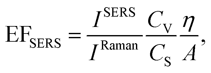
2D ordered arrays of silver nanoprisms were synthesized by nanosphere lithography (NSL).15–17 First, a colloidal monolayer of polystyrene (PS) nanospheres was self-assembled on the surface of a glass substrate according to the method proposed by Giersig and co-workers.26 Commercial PS nanospheres (Microparticles GmbH) with a nominal diameter D = 470 nm were used. All the substrates were previously cleaned in a “piranha” solution (H2SO4![[thin space (1/6-em)]](https://www.rsc.org/images/entities/char_2009.gif) :H2O2, 3:1) for 1 hour at 90 °C, rinsed in ultra-pure deionized water and let dry in air for half an hour. This procedure yields large areas (of the order of some cm2) of patterned substrates. The typical area of the ordered domains of the 2D crystalline monolayer extends up to several hundreds of μm2. After the formation of the colloidal monolayer, silver was thermally evaporated on the samples in orthogonal geometry to form the plasmonic nanoprism arrays. Ag evaporations were performed at a pressure of 5 × 10⁻⁵ mbar with a current of 30 A. The evaporation time was shorter than 300 s. We checked that such conditions do not induce overheating of the PS nanospheres. A calibrated quartz microbalance was used to control the thickness of the evaporated Ag layer (about 100 nm). After the evaporations, the PS nanospheres were mechanically removed by stripping with an adhesive tape. The result of this procedure is an ordered array of triangular nanoprisms (NPA) arranged in a honeycomb lattice on the surface of the glass substrates, as shown in Fig. 1a. The geometric parameters of the nanoprism array were measured by atomic force microscopy and scanning electron microscopy, and are: lattice parameter a0 = 470 ± 10 nm, nanoprisms distance d = 270 ± 6 nm, nanoprisms side length L = 150 ± 3 nm and height h = 98 ± 3 nm. These parameters were used to define the unit cell for the finite elements method (FEM) simulations.
:H2O2, 3:1) for 1 hour at 90 °C, rinsed in ultra-pure deionized water and let dry in air for half an hour. This procedure yields large areas (of the order of some cm2) of patterned substrates. The typical area of the ordered domains of the 2D crystalline monolayer extends up to several hundreds of μm2. After the formation of the colloidal monolayer, silver was thermally evaporated on the samples in orthogonal geometry to form the plasmonic nanoprism arrays. Ag evaporations were performed at a pressure of 5 × 10⁻⁵ mbar with a current of 30 A. The evaporation time was shorter than 300 s. We checked that such conditions do not induce overheating of the PS nanospheres. A calibrated quartz microbalance was used to control the thickness of the evaporated Ag layer (about 100 nm). After the evaporations, the PS nanospheres were mechanically removed by stripping with an adhesive tape. The result of this procedure is an ordered array of triangular nanoprisms (NPA) arranged in a honeycomb lattice on the surface of the glass substrates, as shown in Fig. 1a. The geometric parameters of the nanoprism array were measured by atomic force microscopy and scanning electron microscopy, and are: lattice parameter a0 = 470 ± 10 nm, nanoprisms distance d = 270 ± 6 nm, nanoprisms side length L = 150 ± 3 nm and height h = 98 ± 3 nm. These parameters were used to define the unit cell for the finite elements method (FEM) simulations.
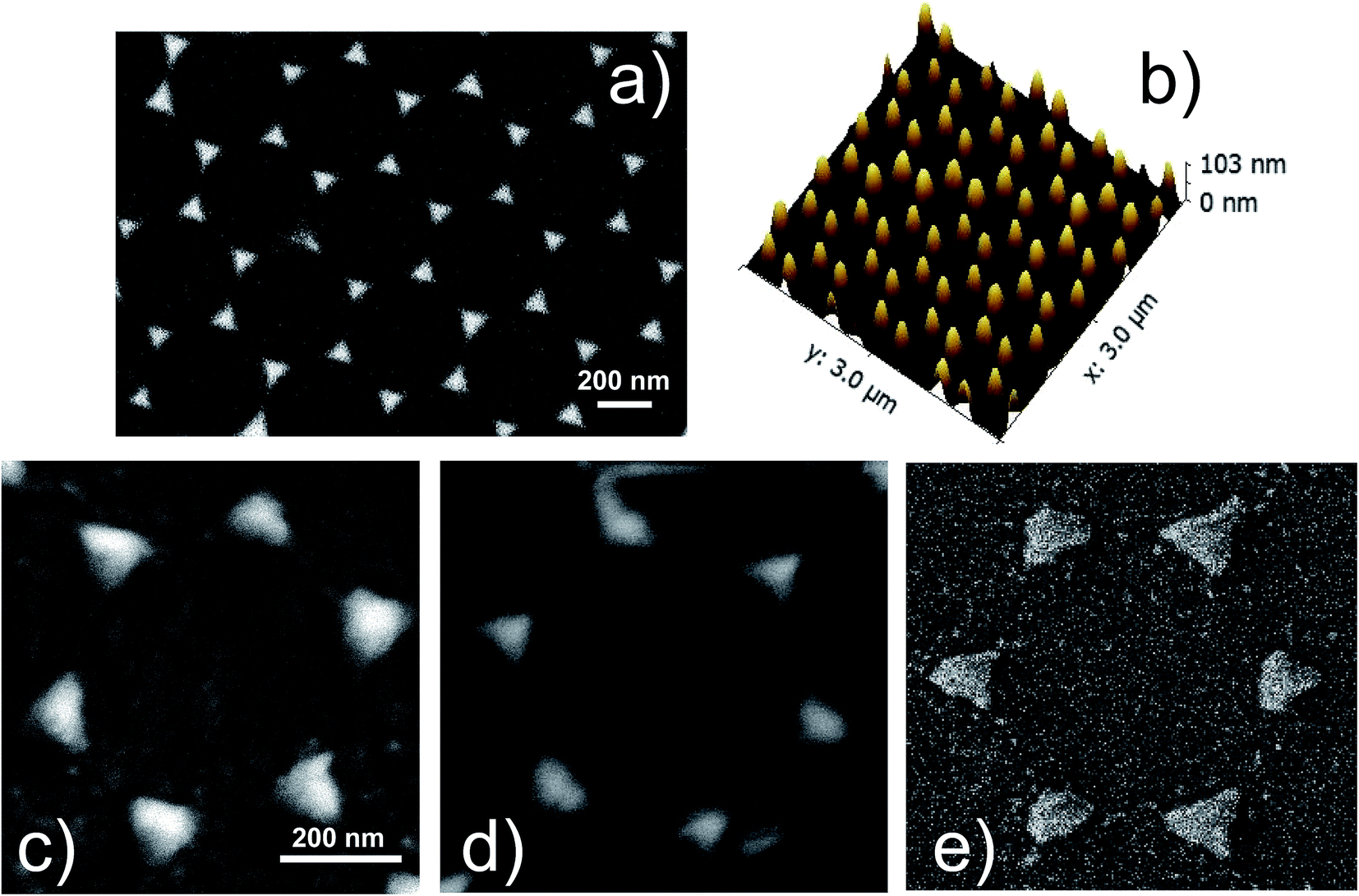 | ||
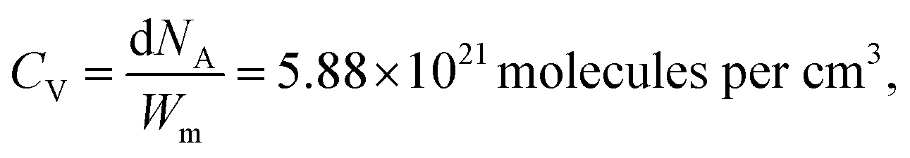
| Fig. 1 (a) SEM image and (b) AFM in 3D-view of a silver nanoprisms array (sample S1-nOx). (c–e) Detail of a SEM image of the NPA in samples S1-nOx (not-oxidized), S2-mOx (mildly oxidized) and S3-sOx (strongly oxidized), respectively. | ||
Structural and optical characterizations
The synthesized nanoprism arrays were characterized morphologically by scanning electron microscopy with a Zeiss SIGMA HD field-emission scanning electron microscope (FE-SEM) operated at 2 kV, with secondary electrons detector. Atomic force microscopy (AFM) measurements were performed using a NT-MDT Solver PRO-M AFM microscope with a 100 × 100 μm scanner, operated in semi-contact mode. Optical absorbance spectra were collected with a JASCO V670 dual beam spectrophotometer. The Ag dielectric function was experimentally determined by ellipsometry measurements performed on continuous films evaporated under the same conditions as those used for the NPAs, using a J. Woollam V-VASE spectroscopic ellipsometer.X-ray photoemission spectroscopy (XPS) data were taken on a VG ESCALAB MKII spectrometer using the Mg anode of a conventional non-monochromatized X-ray source (Kα = 1253.6 eV) and with the analyzer pass energy set to 20 eV. The measurements were taken at room temperature both in normal and grazing emission (55° off from the surface normal). The calibration of the binding energy (BE) scale was determined using the Au 4f XPS peak as reference. Before the measurements the samples have been left degassing in ultra high vacuum conditions overnight.
Samples functionalization
Three identical Ag NPAs (in the following named as S1-nOx, S2-mOx and S3-sOx) were synthesized and functionalized by immersion in a 10 mM solution of benzenethiol (BT) for 15 hours in ambient conditions. After incubation, the SERS substrates were thoroughly washed with methanol in order to remove the excess of benzenethiol. Finally, samples were dried with a nitrogen flux. To study the effect of a different degree of oxidation, sample S1-nOx was functionalized with BT immediately after the synthesis of the nanoprism array (not-oxidized sample), sample S2-mOx was exposed to air at room temperature for a week before functionalization (mildly oxidized sample), while sample S3-sOx was heated at 70 °C in air for 30 minutes before BT functionalization (strongly oxidized sample). These three conditions were chosen to compare realistic situations that can be encountered during normal sample processing, such as possible room temperature aging in air of the samples before their functionalization or intentional oxidation in air at a moderate temperature (<100 °C). Two aspects are important to point out: (i) in addition to thermal oxidation, a morphological reshaping of the triangular nanoprisms may occur, particularly for sample S3-sOx (strongly oxidized); (ii) even for the mildly oxidized sample (S2-mOx), the thermal oxidation process can be expected to proceed more rapidly in the regions with a higher defect density, like the tips or the edges of the nanoprisms. Our aim for the present work is to investigate how the complex interplay of these two aspects globally affect the spectroscopic SERS response of the synthesized silver nanoprism arrays through their influence on the BT functionalization.FEM simulations
Simulations of the linear optical properties (near-field and far-field) of the NPAs have been carried out using a commercial software for finite elements method (FEM)27 computations (COMSOL Multiphysics, version 4.4), as already reported in previous works.18,19 The nanoprism array was modeled by considering a rhombic unit cell (containing 2 nanoprisms) with side a0 and by implementing periodic boundary conditions in the array plane (![[x with combining circumflex]](https://www.rsc.org/images/entities/i_char_0078_0302.gif) y). Each nanoprism was described as a truncated triangular base pyramid of height h = 98 nm, triangular base side length L = 150 nm and triangular top surface side length l = 45 nm. The tip radius was 2 nm. The incident field is described as a plane wave traveling downwards (towards the substrate) along the ẑ axis, orthogonal to the prism triangular base plane, with polarization along the nanoprism center-to-center line. In the ẑ direction the substrate is modeled as semi-infinite. The nanoprisms are placed directly on the substrate and the interface between substrate and the environment is at the z = 0 plane. To model the presence of the benzenethiol monolayer, a conformal layer over the silver nanoprisms (thickness 2 nm, index of refraction n = 1.59, no absorption) was included in the simulations. Over the NPAs the environment (air) is semi-infinite. The semi-infinite conditions are necessary to hinder radiation back-scattering from the external boundaries and are provided by perfectly matched layer sub-domains. The electromagnetic simulation is carried out by solving the Helmholtz equation in the frequency domain. The material properties are described by its relative dielectric permittivity function εr(λ). Magnetic effects are not considered, thus the relative magnetic permeability is μr = 1. For silver, the experimental dielectric function determined by ellipsometric measurements was used, while the refractive index n = 1.59 used for benzenethiol was obtained from the supplier.
y). Each nanoprism was described as a truncated triangular base pyramid of height h = 98 nm, triangular base side length L = 150 nm and triangular top surface side length l = 45 nm. The tip radius was 2 nm. The incident field is described as a plane wave traveling downwards (towards the substrate) along the ẑ axis, orthogonal to the prism triangular base plane, with polarization along the nanoprism center-to-center line. In the ẑ direction the substrate is modeled as semi-infinite. The nanoprisms are placed directly on the substrate and the interface between substrate and the environment is at the z = 0 plane. To model the presence of the benzenethiol monolayer, a conformal layer over the silver nanoprisms (thickness 2 nm, index of refraction n = 1.59, no absorption) was included in the simulations. Over the NPAs the environment (air) is semi-infinite. The semi-infinite conditions are necessary to hinder radiation back-scattering from the external boundaries and are provided by perfectly matched layer sub-domains. The electromagnetic simulation is carried out by solving the Helmholtz equation in the frequency domain. The material properties are described by its relative dielectric permittivity function εr(λ). Magnetic effects are not considered, thus the relative magnetic permeability is μr = 1. For silver, the experimental dielectric function determined by ellipsometric measurements was used, while the refractive index n = 1.59 used for benzenethiol was obtained from the supplier.
To describe the effect of oxidation, the model was modified adding a conformal layer (3 nm thick) of a mixture of silver oxide and benzenethiol on the surface of the silver nanoprisms, whose metallic volume was consequently reduced. The refractive index of the layer was set to the average value between the refractive index of silver oxide (n = 2.5)28,29 and that of BT (n = 1.59). The side length of the modeled nanoprisms was also slightly reduced to L = 140 nm and the tip radius increased to 3 nm, to account for the shape modifications due to oxidation.
SERS measurements
A home-made macro-Raman setup was used to carry out wavelength-scanned surface enhanced Raman spectroscopy measurements (ws-SERS). The system is equipped with a cw Ti:sapphire laser tunable in the range 675–1000 nm (Spectra Physics, 3900S) pumped by a cw optically pumped semiconductor laser (Coherent, Verdi G7) and an Ar+/Kr+ gas laser (Coherent, Innova 70) providing the lines at 488, 514.5, 530.8, 568 and 647.1 nm. The laser lines are filtered through a tunable laser plasma line filter (Laserspec III, Spectrolab) and focused on the sample by a cylindrical lens. The Raman scattering diffused by the sample is collected by a camera objective (CANON 50 mm f/1.2) and coupled into the slit of a three stage subtractive spectrograph (Jobin Yvon S3000) by means of a set of achromatic lenses. The spectrograph is composed of a double monochromator (Jobin Yvon, DHR 320) working as a tunable filter rejecting the elastic scattering and a spectrograph (Jobin Yvon, HR 640). The Raman signal is detected by a liquid nitrogen cooled CCD (Jobin Yvon, Symphony, 1024 × 256 pixels, front illuminated). A polarization scrambler is mounted right in front of the spectrograph slit. The system is configured in backscattering geometry by placing a tiny mirror in front of the collection objective to steer the beam from the cylindrical lens to the sample. The sample is mounted on a translation stage that allows one to move it parallel and perpendicular with respect to the laser propagation direction. The laser power hitting the samples was in the range 1–10 mW for excitation wavelengths up to 740 nm, and in the range 20–45 mW above 740 nm. The spectra were integrated for 10 seconds and averaged out of at least 3 acquisitions.SERS spectra and enhancement factors (EFSERS) were measured in macro-Raman configuration, with a laser spot size of about 3 mm × 80 μm at the sample position. Such spot size is much larger than the one typically used in micro-Raman configuration (which is of the order of a few microns in diameter). The macro-Raman configuration was chosen in order to illuminate an area on the sample similar to the one involved in the measurement of the absorbance spectra. Doing so, in both experiments a very large number of randomly oriented nanoprisms domains are illuminated and possible polarization effects are averaged out. SERS enhancement factors were estimated following the standard procedure outlined by Le Ru,4 by making use of the following relation:
 | (1) |
 where d is the density of liquid BT (d = 1.077 g cm−3), Wm its molecular weight (Wm = 110.19 g mol−1) and NA is the Avogadro number. η is the collection efficiency of the experimental set-up. It was determined by recording the Raman signal at 520 cm−1 of a piece of silicon at several positions along the optical axis (ẑ). The trace was normalized to the maximum and fitted with a Lorentzian profile (L(z)) and η is defined as
  where 2a is the thickness of the reference sample (in this case a 10 mm thick vial). η was measured at each wavelength and was in the range 650–1400 μm. The parameter A is a geometrical factor that accounts for the sample area that is covered with silver and therefore is SERS active. A was calculated as the ratio between the exposed surface (which is covered with Ag) of the 2 nanoprisms in the unit cell and the area of the unit cell. The nanoprisms are considered as truncated triangular base pyramids whose geometrical parameters were defined on the basis of the structural characterizations. For the samples investigated in the present work the estimated value of A is about 0.3. For each sample, the Raman signal was recorded at 10 different points: the EFSERS data and the corresponding error bars were defined as the average value and the standard deviation, respectively.
2 Results and discussion
Fig. 1a shows the SEM image of the Ag nanoprism array of the not-oxidized sample (S1-nOx). In Fig. 1b the AFM image in 3D view of the same sample is reported. A detail of the SEM images of the NPA treated at the different oxidation conditions (not-oxidized, S1-nOx, mildly oxidized, S2-mOx and strongly oxidized, S3-sOx) is shown in panels (c–e). From the morphological point of view the images reveal that the oxidation process does not alter the honeycomb ordered arrangements of the nanoprisms. Only a slight reshaping of the nanotriangles is produced, which is more pronounced in the strongly oxidized sample (S3-sOx, Fig. 1e). The sporadic presence of tiny spherical particles with size of few nanometers around the nanoprisms was observed near some nanoprisms as a by-product of the metal deposition. In principle, due to their very small areal density, their contribution to the SERS signal could be twofold: (i) as single, non-interacting, particles, (ii) as particles interacting with the nanoprisms. In the first case, their SPR resonance is expected to be much more blue-shifted (around 400–450 nm) with respect to the position of the dominant SPR absorbance peak of our samples (630–690 nm, see Fig. 2). In the second case, since they are few, their effect, averaged over all their random relative configurations, is not expected to dominate over the nanoprisms contribution. Therefore, we can safely assume that the contribution of these tiny nanoparticles is not the dominant one and thus in the following we have not included them in the FEM simulations.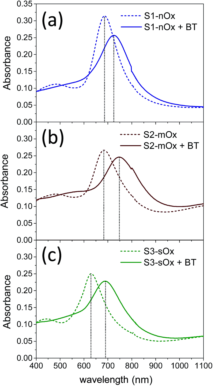 | ||
| Fig. 2 Absorbance spectra of samples S1-nOx (a), S2-mOx (b) and S3-sOx (c) before (dashed lines) and after (solid lines) functionalization with benzenethiol. | ||
Fig. 2 shows the absorbance spectra of the differently oxidized NPAs recorded before (dashed lines) and after (solid lines) functionalization with benzenethiol. Panels (a), (b) and (c) refer to samples S1-nOx, S2-mOx and S3-sOx, respectively. The spectral position of the absorbance maxima measured before and after functionalization, and the corresponding wavelength shifts (ΔλSPR), are summarized in Table 1. Concerning the samples not yet functionalized (dashed curves), the data show a blue-shift of about 55 nm of the absorbance peak of sample S3-sOx (strongly oxidized by thermal treatment in air) with respect to samples S1-nOx and S2-mOx. This behavior can be understood taking into account that counteracting effects may occur in this sample. From one side the formation of an oxide layer on the surface of the nanoprisms is expected to red-shift the surface plasmon resonance due to the increase of the dielectric function, but on the other hand the reduced volume of metallic silver (due to surface oxidation) together with the reshaping of the nanoprisms, and in turn the diminished interaction between the nanoprisms, produce a blue-shift of the SPR peak. The latter effects resulted to be the dominant ones in this sample.
| Samples | Absorbance | ws-SERS | |||||
|---|---|---|---|---|---|---|---|
| Before λSPRmax (nm) | After λSPRmax (nm) | ΔλSPR (nm) | EFSERS × 106 | λSERSmax (nm) | ΔλSERS (nm) | EFSERS (@700 nm) × 106 | |
| S1-nOx | 686 | 723 | +37 | 4.5 ± 0.9 | 702 | −21 | 4.5 ± 0.9 |
| S2-mOx | 683 | 748 | +65 | 1.8 ± 0.2 | 723 | −25 | 1.6 ± 0.2 |
| S3-sOx | 629 | 690 | +61 | 2.1 ± 0.2 | 677 | −13 | 2.0 ± 0.2 |
After functionalization with benzenethiol all the samples showed red-shifted absorbance spectra (solid curves), and such an effect was more pronounced (by about a factor of 2) on the oxidized samples with respect to the not-oxidized one. These data indicate that benzenethiol effectively binds to the oxidized surface as it does to the metal surface. This finding is confirmed also in several studies in the literature. As an example, in ref. 31 Himmelhaus and co-workers investigated by X-ray Photoelectron Spectroscopy (XPS) the interaction of aliphatic thiols in ethanol solution with polycrystalline silver substrates possessing a native layer of oxide. The authors demonstrated that the aliphatic thiols can reduce the silver oxide leading to the formation of chemisorbed alkanethiolate. By studying the adsorbed amount as a function of the oxygen coverage on the surface by varying the exposure time of fresh silver substrates to air prior to functionalization, they concluded that the higher is the amount of oxygen initially present, the higher is the adsorbed amount of thiol. Furthermore, in ref. 32 and 33 Laibinis and co-authors proved that the immersion of a silver film with a thin layer of oxide in an alkylthiol solution leads to the almost complete displacement/reduction of oxygen and the formation of a self-assembled monolayer.
Fig. 3a shows a comparison between the Raman spectrum of liquid benzenethiol (red line) and of sample S1-nOx functionalized with BT (blue line). The spectra were recorded with laser excitation at λL = 710 nm, under the same experimental conditions. The laser power on the sample was 5 mW, the integration time 10 s and each spectrum was the average of 10 acquisitions. In order to calculate the SERS enhancement factor (EFSERS), we referred to the Δω = 999 cm−1 band. In Fig. 3b–d the ws-SERS data for the three differently oxidized samples, S1-nOx, S2-mOx and S3-sOx, are reported together with the corresponding experimental absorbance spectra: the gray dots are the experimental EFSERS values and the orange line is the Lorentzian fit to the EFSERS data. The wavelengths at which the maximum EFSERS is measured (λSERSmax) and the corresponding value for the three samples are reported in Table 1. To allow for a comparison of the SERS response of the samples at the same wavelength, in the last column of Table 1 we have also reported, for the three samples, the values of EFSERS measured at 700 nm, i.e., at the wavelength at which the SERS enhancement of the not-oxidized sample is maximum. ΔλSERS indicates the spectral difference between the maximum in the EFSERS profiles and the absorbance peak of the functionalized samples. The data show a blue-shift of the EFSERS profile with respect to the absorbance spectrum for all the three investigated samples. This behavior can be understood considering that the SERS enhancement factor is proportional to the product E2(λL)E2(λR), where λR = (1/λL − Δω)−1 is the Raman shifted emission wavelength, and not merely to E4(λL). Since λR > λL, the EFSERS peak occurs at a shorter wavelength if plotted against λL. This effect is well known and has been demonstrated experimentally in ref. 8 and 11.
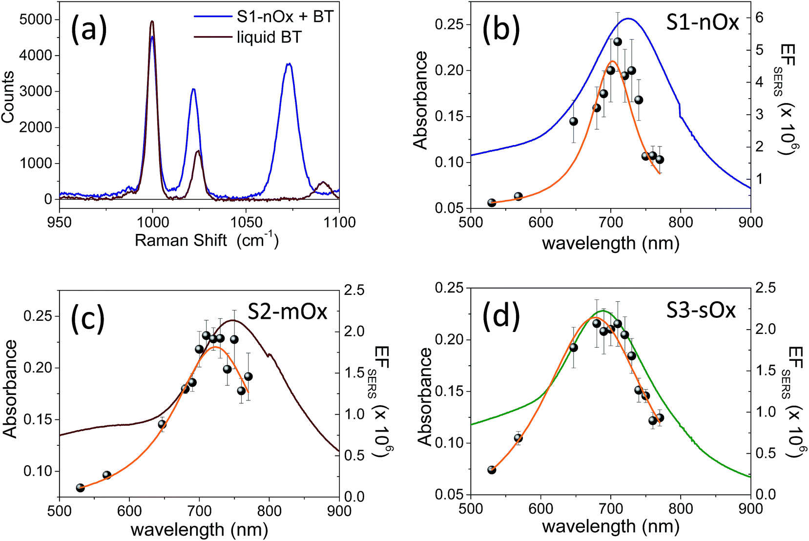 | ||
| Fig. 3 (a) Raman spectra of liquid BT (red) and BT absorbed on sample S1-nOx (blue). The spectra have been recorded with excitation at λexc = 710 nm under the same experimental conditions; the laser power on the samples was 5 mW, the integration time 10 s and each spectrum was the average of 10 acquisitions. (b), (c), (d) Absorbance spectra (blue, red and green lines), experimental SERS enhancement factors (gray dots) and Lorentzian fit (orange line) of samples S1-nOx, S2-mOx and S3-sOx, respectively. | ||
Concerning the role of oxidization, first of all by comparing the results of sample S2-mOx (Fig. 3c) with those of sample S1-nOx (Fig. 3b), it emerges that the atmospheric oxidation gives rise to a spectral shift of the EFSERS profile with respect to the absorbance spectrum as in the not-oxidized sample (S1-nOx), but the maximum SERS enhancement factor results reduced by a factor of 2.5. Sample S3-sOx instead, with respect to S1-nOx, exhibits a smaller blue-shift of the EFSERS profile, but a reduction of the maximum enhancement factor similar to sample S2-mOx (by a factor of 2.5). To understand the observed difference in the maximum EFSERS between fresh and oxidized samples, the effect of the presence of an oxide layer on the following factors has to be taken into account: (i) in calculating the experimental EFSERS we assumed the same surface density for BT in all the samples, but the affinity of benzenethiol to metal and oxide in principle could be different; (ii) the strength of the chemical enhancement, as defined in ref. 1, may be different when the molecule is bound to the metal rather than to the oxide layer; (iii) the electromagnetic enhancement decreases steeply with the distance from the plasmonic material, therefore it can be affected by the possible presence of a dielectric layer acting as a spacer; (iv) the oxidation process slightly modifies the morphology of the substrates, as shown in Fig. 1c–e, and thus it can alter distribution and intensity of the electric field. Since these factors are not all in the direction of inducing a decrease of the SERS signal, their overall effect may cause no major drops in the enhancement factor but a more limited reduction, as experimentally observed. Therefore, in order to completely unveil the role of the different parameters on the SERS response, a deep analysis of the electrodynamic effects was performed by finite elements method (FEM) simulations.
FEM simulations were used to compute the local-field distributions and the NPA far-field properties. It is worth noting that for the simulated geometries, whose parameters were chosen on the basis of the FE-SEM and AFM characterizations, the spectral position of the maximum of the calculated absorbance is coincident with that of the simulated absorption. This confirms that we can use the experimentally measured absorbance maximum as representative of the experimental absorption maximum of the samples. The SERS enhancement factor (EFSERS) was calculated by using the local-field distribution inside the volume of the analyte layer (BT) both for excitation and Raman shifted emission frequencies. A sketch of the local-field distribution at the wavelength of the maximum of the simulated absorbance spectrum of sample S1-nOx is given in Fig. 4. The figure shows that intense hot-spots of the electromagnetic field are formed at the nanoprisms tips, further enhanced by the near-field coupling among the nanotriangles, with an enhancement of the modulus of the local electric field (normalized to the incident field, E0) up to a factor 1000.
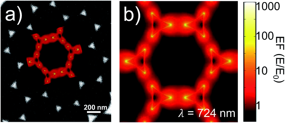 | ||
| Fig. 4 (a) SEM image of sample S1-nOx and (b), and as inset in (a), simulated map of the local-field enhancement calculated at the indicated wavelength (corresponding to the maximum of the simulated absorbance spectrum). | ||
Inside the active layer the local SERS enhancement factor has been computed as a function of the local electric field E(r,ω):
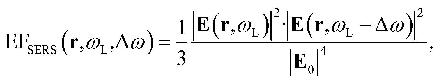 | (2) |
 | (3) |
The computed SERS enhancement factor is thus dependent on two parameters: the incident light frequency, ωL, and the Raman shift, Δω. The simulations were carried out considering the experimentally probed Raman shift of benzenethiol, Δω = 999 cm−1. In Fig. 5a the EFSERS spectrum of sample S1-nOx (not-oxidized), computed using eqn (3), is reported (red curve, left-hand scale) and compared to its simulated absorbance spectrum (orange curve, right-hand scale). Concerning the EFSERS profile, as previously discussed the maximum of the SERS enhancement curve is expected to be shifted towards higher energies (i.e., shorter wavelengths) with respect to the absorbance peak and this is indeed confirmed by the simulations. Furthermore, by comparing the results of the simulations to the experimental ones of sample S1-nOx (Fig. 3b), the first thing to note is the very good agreement between the measured and calculated values of the maximum EFSERS, which is close to 5 × 10⁶ in both cases. The spectral position of the simulated EFSERS peak results instead slightly blue-shifted with respect to the experimental one. This behavior can be explained taking into account the great inhomogeneity of the electric-field distribution within the NPA surface (see Fig. 4b). In nanostructures like the nanoprisms investigated in the present work, in which there are small regions with high curvature (i.e., the nanoprism tips), the maximum local electric-field at the tips in general does not occur at the same wavelength as in the whole nanoprism. Particularly, in the present case, close to the tips the maximum field enhancement takes place at shorter wavelengths. Moreover, from one hand the high-curvature regions produce the hottest spots in the electric-field but, on the other hand, the small extent of these regions reduces their integrated contribution in the average of the field over the total volume of the nanoprism. Absorbance is a linear property and it is sensitive to the average electric-field in the NPAs rather than the hottest spots, whereas the hot-spots dominate in the average of higher powers of the field-enhancement, as it is for the SERS enhancement. As a consequence, the highest EFSERS occurs where the convolution of the incident and the Raman shifted curves of the square of the enhancement factor (where the hot-spot regions have more weight), averaged over the volume of the BT layer (〈(E/E0)2〉), is maximum rather than where the convolution of the absorbance curves is maximum. Since, as shown in Fig. 5a (blue curve), the simulated spectrum of 〈(E/E0)2〉 is maximum at shorter wavelengths with respect to the absorbance one, this accounts for the larger blueshift of the EFSERS maximum resulting from the simulations. As regards the experimental results, instead, it is important to point out that the possible presence of defects in the samples may hinder the spectral decoupling of the maximum squared electric-field enhancement from the maximum absorbance and this could be the reason why the experimental EFSERS peak (702 nm) was found to be red-shifted with respect to the simulated one (688 nm) and close to the middle of the absorbance peaks evaluated at λL and λR (700 nm). Moreover, the presence of defects in the experimental sample could account also for the larger width of the experimental EFSERS curve with respect to the simulated one.
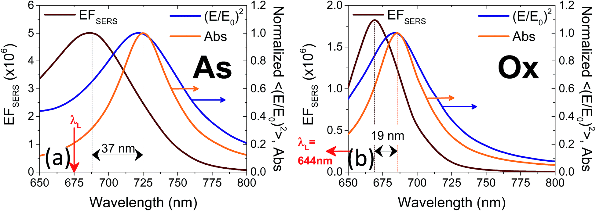 | ||
| Fig. 5 Normalized absorbance spectrum (orange line, right-hand scale), normalized profile of the square of the local-field enhancement factor 〈(E/E0)2〉 averaged over the BT layer (blue line, right-hand scale) and EFSERS profile (red line, left-hand scale) obtained by FEM simulations of (a) sample S1-nOx (not-oxidized, As-deposited) and (b) sample S3-sOx (oxidized, Ox) functionalized with BT. In both panels the red arrows indicate the incident laser wavelength needed to get the maximum absorption at the Raman shifted wavelength. | ||
FEM simulations were carried out also to describe the effect of oxidation. In this case, the model has been modified assuming a conformal, 3 nm thick, layer representing a mixture of silver oxide and BT, as foreseen in an interaction scheme where the oxide is permeable to the binding of BT with metallic silver. The reduced sharpness of the nanoprisms observed in the oxidized sample was modeled by increasing the tip curvature radius to about 3 nm and reducing the prisms side length to L = 140 nm. The thickness of the oxide/BT layer was fixed at the value that reproduced in the simulations the spectral shift of the absorbance spectrum observed as a consequence of the oxidation process. In the attempt to provide a direct, experimental determination of the thickness of the oxide layer, XPS measurements were performed both on nanostructured samples as those investigated here (synthesized on Si substrates to minimize surface charging), and on continuous Ag films (as-deposited and strongly oxidized with the same procedure used for the nanoprism arrays, and also oxidized and functionalized with benzenethiols) to be used as a benchmark. Unfortunately, our attempts were stalled by some inherent technical limitations. As a matter of fact, the chemical shift of the Ag 3d photoemission line for Ag and Ag2O is very small, of about +0.3 to 0.4 eV,34,35 and therefore it is very hard to detect by using standard sources (i.e. without synchrotron radiation). The analysis of the O 1s photoemission line is equally complex: up to five types of different oxygen atoms can be observed on oxidized Ag surfaces (i.e. strongly and weakly bound, oxygen diluted in the bulk and related to different sources of intrinsic contamination) even on single crystals in ultra-high vacuum studies. All these difficulties are further enhanced for the nanostructured samples. Therefore, in the following we restricted the XPS analysis to the ideal, planar films. The body of our photoemission measurements indicate the presence of Ag in metal form (as determined by the position of the Ag 3d 5/2 maximum and Auger parameter) and no distinct oxide component that could be associated with Ag2O could be detected (see Fig. 6a). Similarly, from the analysis of the O 1s photoemission line it was not possible to clearly identify the presence of an oxide component (Fig. 6b). Moreover, comparative measurements did not outline any difference between grazing and normal emission acquisitions and between different samples (that is, the as-deposited sample vs. the sample oxidized at 70 °C in air). On the other hand, by means of photoemission we were able to easily verify the presence of the thiol on the oxidized and thiolated surface revealed by the S 2p peak whose position at 162.0 eV is typical of surface thiolates (Ag–S–C, not reported). Therefore, the demonstrated inherent difficulties to detect Ag–O species in the samples by XPS characterization (which in principle is expected to be the elective technique for assessing Ag–O bonding) have prevented us to get a reliable measurement of the thickness of the oxide layers by angle resolved photoemission measurements and to decouple the role of shape changes from that of thermal oxidation. For this reason, our approach was to follow the oxidation process by FEM simulations of the change in the optical properties of the samples due to both morphological and dielectric modifications of the nanoprisms.
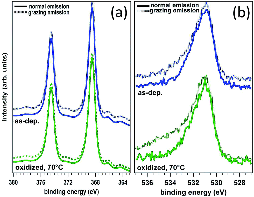 | ||
| Fig. 6 Ag 3d spectra (a) and O 1s spectra (b) of silver films, both as-deposited and intentionally oxidized at 70 °C, 30 min in air. | ||
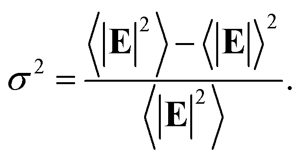
In the following we restricted the discussion to the comparison between experimental results and FEM simulations of the two “extreme” samples, S1-nOx (not-oxidized) and S3-sOx (strongly oxidized), which represent the most different configurations in terms of SERS response. As reported in Table 1, the effect of oxidation of the NPAs on the SERS response is two-fold: (i) the maximum experimental EFSERS measured in the oxidized samples is reduced by a factor ∼2.5 with respect to the fresh (not-oxidized) sample; (ii) in sample S3-sOx (strongly oxidized) the spectral position of the maximum experimental EFSERS is blue-shifted with respect to the corresponding absorbance peak (ΔλSERS) to a lesser extent than for samples S1-nOx and S2-mOx (13 nm for S3-sOx vs. 21 nm for S1-nOx). Both these features were recovered by the simulations, as shown in Fig. 5b. The reduction in the EFSERS is the result of two effects. From one side, the presence of a dielectric layer with higher refractive index (due to the presence of the oxide) helps in confining the field close to the nanostructures surface giving rise to an increase of the local electric field due to dielectric coupling. On the other side, the reduced sharpness of the metallic part of the nanostructure reduces the field enhancement in the hot-spot regions, thus taking to a decrease of the average local electric field, and to its more homogeneous distribution. From the simulations, a decrease of the EFSERS of a factor ∼2.7 is obtained which is in very good agreement with the factor ∼2.5 observed experimentally for the oxidized samples. The origin of the reduced blue-shift in the strongly oxidized sample (S3-sOx) is more subtle. As already pointed out for the not-oxidized sample S1-nOx, the blue-shift is caused by two factors, i.e., (i) the convolution of the resonances evaluated at the incident laser wavelength (λL) and at the Raman-shifted one (λR) and (ii) the enhanced contribution of the hot-spot regions due to the strong inhomogeneity in the field distribution. In the oxidized sample, the convolution effect is still present and works in the same way. Concerning the second factor, on the other hand, the simulations proved that the reduced sharpness and the presence of the oxide layer give rise to a more homogeneous field distribution. An estimate of the inhomogeneity of the field can be calculated using the normalized variance of the electric field inside the oxide/BT volume (angle brackets indicate the average over the oxide/BT layer volume):
 | (4) |
Computing the variance at the wavelength where the absorbance is maximum for each sample, we obtained: σfresh2(λmax) = 0.87 > σoxidized2(λmax) = 0.76, with a relative difference of about 15%. As a consequence of this, the EFSERS curve is blue-shifted with respect to the absorbance spectrum to a lesser extent in the strongly oxidized sample than in the not-oxidized one. Particularly, both the simulations and the experiment proved a reduction of the blue-shift in the oxidized sample of about half the blue-shift of the not-oxidized one: from the simulations (experiment) we obtained a blue-shift of −19 nm (−13 nm) for the oxidized sample (S3-sOx), with respect to −37 nm (−21 nm) for the not-oxidized one (S1-nOx). Moreover, the width of the EFSERS curve peak results slightly reduced in the simulations when the oxide is present. This is a further effect of the increased homogeneity in the local electric field distribution in this condition. Nonetheless, experimentally this behavior is not observed. Indeed, the width of the experimental EFSERS profile results larger for the oxidized sample than for the not-oxidized one (Fig. 3d and b). This could be explained considering two aspects: on one hand, the presence of defects in the experimental sample gives rise to a wider absorbance peak than the simulated one, which causes an enlargement of the EFSERS profile, as already noted for the not-oxidized sample; besides this, a possible not-uniform distribution of benzenethiol over the surface of the nanoprisms (which could also vary among the nanoprisms) has to be taken into account. Both these effects produce an inhomogeneous broadening of the EFSERS profile in the experimental sample, and thus an enlargement of the peak, which is absent in the simulated (perfect) case.
3 Conclusions
Wavelength-scanned SERS measurements were performed on Ag nanoprism arrays with a different degree of oxidation and functionalized with benzenethiol to determine the SERS enhancement curves as a function of the incident laser wavelength around the dipolar surface plasmon resonance of the arrays. The experimental findings were compared with the results of FEM simulations. The effect of oxidation was modeled assuming a 3 nm thick conformal layer of silver oxide and benzenethiol at the surface of the nanoprisms. An excellent agreement between the experimental and the simulated data was obtained and the results were interpreted on the basis of the inhomogeneities of the electromagnetic field distribution around the nanoprisms.In summary, the main findings are:
(i) A spectral blue-shift of the SERS enhancement profiles with respect to the corresponding absorbance spectra is observed both experimentally and from FEM simulations.
(ii) The extent of the blue-shift is related to the oxidation process and resulted smaller in the strongly oxidized sample than in the not-oxidized one.
(iii) The simulations proved that the reduced nanoprism tip sharpness and the presence of the oxide layer give rise to a more homogeneous field distribution around each nanoprism, which in turn provides an explanation for the smaller blue-shift observed in the oxidized sample.
(iv) Concerning the absolute values of the SERS enhancement, a decrease of about a factor of 2.5 of the maximum SERS enhancement factor is measured for the oxidized samples, which is consistently proved by FEM simulations.
In conclusion, from a practical standpoint we can state that the tendency of silver towards oxidation does not preclude the use of Ag NPAs as platforms for SERS sensing with thiol-terminated molecules. Benzenethiol was found to effectively bind to the oxidized NPA surface as it does to the metallic NPAs: the EFSERS reduction demonstrated in the oxidized samples amounts only to a factor of 2.5 and therefore does not alter significantly the NPA performances required for applications.
Acknowledgements
This work has been partially supported by the Progetto di Ateneo CPDA101587 of the University of Padova, Italy. The support from the Progetto di Grande Rilevanza Italia-Messico MX14MO09 of the Ministero degli Affari Esteri e della Cooperazione Internazionale (MAECI) of Italy is also acknowledged.References
- E. C. Le Ru and P. G. Etchegoin, Principles of Surface-Enhanced Raman Spectroscopy, Elsevier, Amsterdam, The Nederlands, 2009 Search PubMed.
- J. Kneipp, H. Kneipp and K. Kneipp, Chem. Soc. Rev., 2008, 37, 1052–1060 RSC.
- E. C. Le Ru and P. G. Etchegoin, Annu. Rev. Phys. Chem., 2012, 63, 65–87 CrossRef CAS PubMed.
- E. Le Ru, E. Blackie, M. Meyer and P. G. Etchegoin, J. Phys. Chem. C, 2007, 111, 13794–13803 CAS.
- G. Giallongo, R. Pilot, C. Durante, G. A. Rizzi, R. Signorini, R. Bozio, A. Gennaro and G. Granozzi, Plasmonics, 2011, 6, 725–733 CrossRef CAS.
- G. Giallongo, C. Durante, R. Pilot, D. Garoli, R. Bozio, F. Romanato, A. Gennaro, G. Rizzi and G. Granozzi, Nanotechnology, 2012, 23, 325604 CrossRef CAS PubMed.
- F. Romanato, R. Pilot, M. Massari, T. Ongarello, G. Pirruccio, P. Zilio, G. Ruffato, M. Carli, D. Sammito, V. Giorgis, D. Garoli, R. Signorini, P. Schiavuta and R. Bozio, Microelectron. Eng., 2011, 88, 2717–2720 CrossRef CAS.
- A. D. McFarland, M. A. Young, J. A. Dieringer and R. P. Van Duyne, J. Phys. Chem. B, 2005, 109, 11279–11285 CrossRef CAS PubMed.
- S. L. Kleinman, B. Sharma, M. G. Blaber, A.-I. Henry, N. Valley, R. G. Freeman, M. J. Natan, G. C. Schatz and R. P. Van Duyne, J. Am. Chem. Soc., 2013, 135, 301–308 CrossRef CAS PubMed.
- R. Pilot, A. Zoppi, S. Trigari, F. L. Deepak, E. Giorgetti and R. Bozio, Phys. Chem. Chem. Phys., 2015, 17, 7355–7365 RSC.
- V. Weber, A. Feis, C. Gellini, R. Pilot, P. R. Salvi and R. Signorini, Phys. Chem. Chem. Phys., 2015, 17, 21190–21197 RSC.
- E. Le Ru and P. Etchegoin, Principles of Surface-Enhanced Raman Spectroscopy and Related Plasmonic Effects, Elsevier, 2008 Search PubMed.
- M. Erol, Y. Han, S. K. Stanley, C. M. Stafford, H. Du and S. Sukhishvili, J. Am. Chem. Soc., 2009, 131, 7480–7481 CrossRef CAS PubMed.
- Y. Han, R. Lupitskyy, T.-M. Chou, C. M. Stafford, H. Du and S. Sukhishvili, Anal. Chem., 2011, 83, 5873–5880 CrossRef CAS PubMed.
- J. C. Hulteen, D. A. Treichel, M. T. Smith, M. L. Duval, T. R. Jensen and R. P. Van Duyne, J. Phys. Chem. B, 1999, 103, 3854–3863 CrossRef CAS.
- C. L. Haynes and R. P. Van Duyne, J. Phys. Chem. B, 2001, 105, 5599–5611 CrossRef CAS.
- L. Brigo, N. Michieli, L. Artiglia, C. Scian, G. A. Rizzi, G. Granozzi, G. Mattei, A. Martucci and G. Brusatin, ACS Appl. Mater. Interfaces, 2014, 6, 7773–7781 CAS.
- N. Michieli, B. Kalinic, C. Scian, T. Cesca and G. Mattei, Biosens. Bioelectron., 2015, 65, 346–353 CrossRef CAS PubMed.
- T. Cesca, N. Michieli, B. Kalinic, A. Sànchez-Espinoza, M. Rattin, V. Russo, V. Mattarello, C. Scian, P. Mazzoldi and G. Mattei, Nanoscale, 2015, 7, 12411–12418 RSC.
- G. Perotto, V. Bello, T. Cesca, G. Mattei, P. Mazzoldi, G. Pellegrini and C. Scian, Nucl. Instrum. Methods Phys. Res., Sect. B, 2010, 268, 3211–3214 CrossRef CAS.
- J. Zheng and L. He, Compr. Rev. Food Sci. Food Saf., 2014, 13, 317–328 CrossRef CAS.
- D. S. Grubisha, R. J. Lipert, H.-Y. Park, J. Driskell and M. D. Porter, Anal. Chem., 2003, 75, 5936–5943 CrossRef CAS PubMed.
- K. C. Bantz, A. F. Meyer, N. J. Wittenberg, H. Im, z. Kurtulus, S. H. Lee, N. C. Lindquist, S.-H. Oh and C. L. Haynes, Phys. Chem. Chem. Phys., 2011, 13, 11551–11567 RSC.
- K. Ma, J. M. Yuen, N. C. Shah, J. T. Walsh, M. R. Glucksberg and R. P. Van Duyne, Anal. Chem., 2011, 83, 9146–9152 CrossRef CAS PubMed.
- S. Schlücker, Angew. Chem., Int. Ed., 2014, 53, 4756–4795 CrossRef PubMed.
- J. Rybczynski, U. Ebels and M. Giersig, Colloids Surf., A, 2003, 219, 1–6 CrossRef CAS.
- J. Jin, J. Jin and J. Jin, The finite element method in electromagnetics, Wiley, New York, 2nd edn, 2002 Search PubMed.
- J. Tominaga, J. Phys.: Condens. Matter, 2003, 15, R1101 CrossRef CAS.
- A. A. Schmidt, J. Offermann and R. Anton, Thin Solid Films, 1996, 281–282, 105–107 CrossRef CAS.
- T. H. Joo, M. S. Kim and K. Kim, J. Raman Spectrosc., 1987, 18, 57–60 CrossRef CAS.
- M. Himmelhaus, I. Gauss, M. Buck, F. Eisert, C. Wöll and M. Grunze, J. Electron Spectrosc. Relat. Phenom., 1998, 92, 139–149 CrossRef CAS.
- P. E. Laibinis, G. M. Whitesides, D. L. Allara, Y. T. Tao, A. N. Parikh and R. G. Nuzzo, J. Am. Chem. Soc., 1991, 113, 7152–7167 CrossRef CAS.
- P. E. Laibinis, M. A. Fox, J. P. Folkers and G. M. Whitesides, Langmuir, 1991, 7, 3167–3173 CrossRef CAS.
- X. Bao, M. Muhler, T. Schedel-Niedrig and R. Schlögl, Phys. Rev. B: Condens. Matter Mater. Phys., 1996, 54, 2249–2262 CrossRef CAS.
- T. C. R. Rocha, A. Oestereich, D. V. Demidov, M. Hävecker, S. Zafeiratos, G. Weinberg, V. I. Bukhtiyarov, A. Knop-Gericke and R. Schlögl, Phys. Chem. Chem. Phys., 2012, 14, 4554 RSC.
Footnote |
| † These authors contributed equally to this work. |
| This journal is © The Royal Society of Chemistry 2017 |