
 Open Access Article
 This Open Access Article is licensed under a
 Creative Commons Attribution 3.0 Unported Licence
Recrystallization of copper at a solid interface for improved CVD graphene growth†
Ya-Ping Hsieh *a,
Ding-Rui Chena,
Wan-Yu Chianga,
Kai-Jyun Chenb and
Mario Hofmannb
*a,
Ding-Rui Chena,
Wan-Yu Chianga,
Kai-Jyun Chenb and
Mario Hofmannb
aGraduate Institute of Opto-Mechatronics, National Chung Cheng University, Chiayi, 62102, Taiwan. E-mail: yphsieh@ccu.edu.tw
bDepartment of Material Science and Engineering, National Cheng Kung University, Tainan, 70101, Taiwan. E-mail: Mario@mail.ncku.edu.tw
First published on 13th January 2017
Abstract
The quality of CVD-grown graphene is intimately linked to the morphology of the employed catalyst. One commonly employed route to enhanced catalyst quality is recrystallization prior to graphene growth. The dimensions of a catalyst's single-crystalline domains, however, are limited by the stability of dislocations at the grain boundaries. We here employ a solid material in contact with the catalyst as a sink for dislocations. It was found that the interaction between Cu-foil and a solid cap significantly alters the recrystallization kinetics and achievable grain size. This development originates from an improved strain-relaxation of up to 1% during recrystallization which can support the formation of commonly unstable surface orientations. Correlation of diffraction measurements and atomic force microscopy reveals a direct impact of the strain relaxation on the decrease in copper surface roughness. Finally, we demonstrate the improvement of the quality of graphene grown on thus prepared foils through spectroscopic and carrier transport measurements.
Introduction
Graphene is a two-dimensional nanomaterial that has been heralded as an enabling material for novel electronic devices, sensors, and transparent conductors.1 To fulfill requirements in these areas, the increase in graphene quality and crystallinity synthesized by chemical vapor deposition (CVD) is the focus of ongoing efforts.One important aspect that was found to affect graphene's domain size, domain orientation, and carrier mobility, is the crystallinity of the underlying catalyst surface.2–5 Previous reports showed that the smoothness of Cu will dominate the defect density of graphene.6–9 Moreover, Cu grain boundaries act as obstacles to graphene growth10–12 and deteriorate graphene's quality.12 Therefore, an ideal substrate for high quality graphene growth needs to have larger Cu grains.
Several studies demonstrated that the grain size of commonly used Cu foil can be enhanced by annealing prior to CVD growth.13–15 This grain growth occurs due to the presence of large amounts of strain that are introduced during the foil production process.16,17 Grain growth then proceeds through recrystallization which displaces dislocations in the lattice and thus releases the strain.18 The grain growth seizes, however, when dislocation motion and grain boundary motion reach an equilibrium.19
To overcome this fundamental limitation, we require a method to affect the concentration of dislocations and thus change the equilibrium condition. One such way is the introduction of a sink of dislocations. If dislocations are removed from the grain boundaries, grain growth could proceed further and significantly larger grains are achievable.20
We here demonstrate that a solid interface in contact with the Cu foil can act as such a sink for dislocations. By placing a solid cap onto the Cu foil, the recrystallization process was found to be significantly altered. Electron back scatter diffraction (EBSD) showed a slower recrystallization process and larger achievable final grain size. This behavior was found to be caused by an enhanced strain relaxation at the Cu/solid interface. The observed stress relaxation furthermore lowers the roughness of Cu and ultraflat surfaces with Ra < 0.4 nm were obtained. Finally, graphene grown on these cap-annealed copper substrates were found to have larger grain sizes and an enhanced carrier mobility.
Experimental
Graphene was grown on 25 μm thick foil copper foil (Alfa Aesar 46365, purity 99.8%) following established procedures.21Annealing was carried out using an atmosphere of argon and hydrogen with a volume ratio of 7![[thin space (1/6-em)]](https://www.rsc.org/images/entities/char_2009.gif) :2 at a pressure of 700 Torr for various times. During annealing, caps of graphite were placed on top of one Cu foil while an uncapped Cu foil was exposed to the same annealing process (Fig. 1) and an additional weight (quartz, 7 g) was place on top of graphite to increase the contact between copper and graphite.
:2 at a pressure of 700 Torr for various times. During annealing, caps of graphite were placed on top of one Cu foil while an uncapped Cu foil was exposed to the same annealing process (Fig. 1) and an additional weight (quartz, 7 g) was place on top of graphite to increase the contact between copper and graphite.
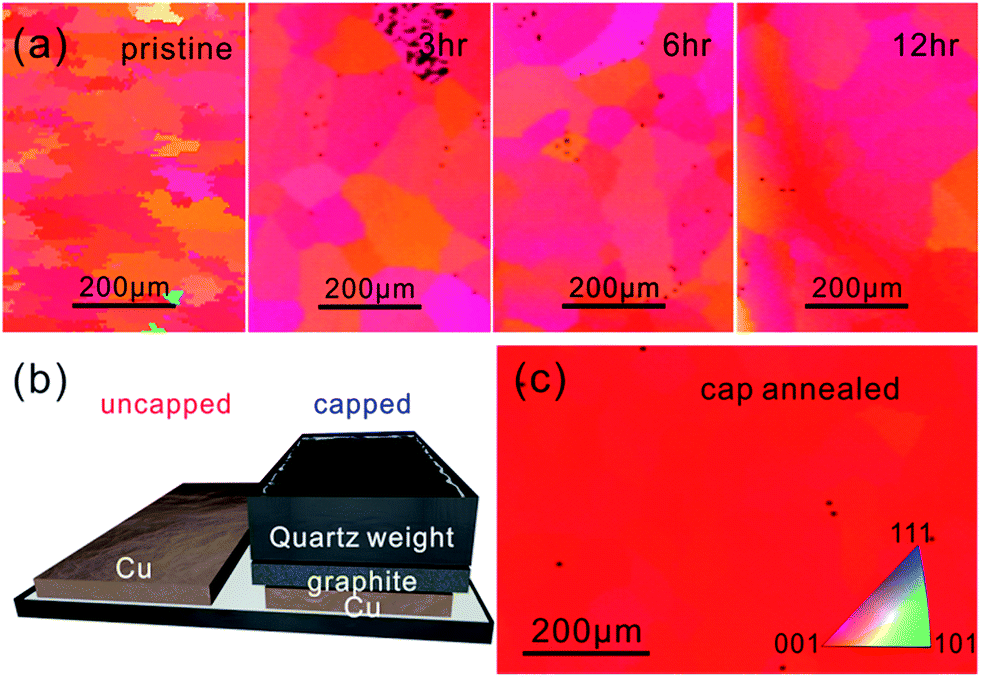 | ||
| Fig. 1 (a) EBSD images before and during uncapped annealing (b) schematic of capped annealing process, (c) EBSD of Cu foil after 8 hours capped annealing. | ||
Afterwards, AFM images were taken (FORCE Genie) and the roughness of copper was analyzed using the Gwyddion software package.
The texture and grain boundary distribution of the copper were examined by electron back scattering diffraction (EBSD, JSM 7001F) operating at 20 kV. X-ray diffraction was carried out on a Bruker D2 Phaser for more than 4 different samples for each process condition and peak positions were averaged after individual fitting.
Graphene was grown under a flow of 200 sccm hydrogen and 10 sccm methane at 10 Torr following previous reports.21 Two different growth durations (20 min and 6 hours) were used to obtain separate grains and well-connected films, respectively.
Mobility of graphene was extracted from field effect transistors (FETs) with channel lengths of 150 μm which were fabricated on SiO2-supported graphene by deposition of gold through a shadow mask. The field effect mobility was extracted following previous reports.22
To visualize graphene on copper under an optical microscope (OM), graphene-covered copper was first air oxidized following previous report.23
Results and discussion
Electron back scatter diffraction (EBSD) of the pristine Cu surface shows small size of grains (∼50 μm) with a predominantly (100) oriented surface and few higher angle textures (Fig. 1(a)).We find that the grain size of Cu increases with annealing time in agreement with previous reports.13 However, even after 12 h annealing the grain size is below 200 μm.
This behavior is in marked difference with samples that were brought in contact with a solid cap and annealed under the same conditions (see Fig. 1(b)). We observe a consistent increase of grain size compared to uncapped annealing under identical conditions. After 12 hours annealing most cm-sized samples did not exhibit any grain boundaries indicating complete conversion into single crystals (Fig. 1(c)).
In order to understand this behavior, we carried out 3 hour annealing experiments at different temperatures for capped and uncapped Cu foil. Fig. 2(a) shows an Arrhenius plot of the grain dimension as a function of inverse temperature extracted from backscattered electron imaging (BEI) (ESI Fig. S1†) and a clear linear trend is observed which suggests a temperature activated diffusion process to dominate the grain growth in both capped and uncapped annealing conditions.
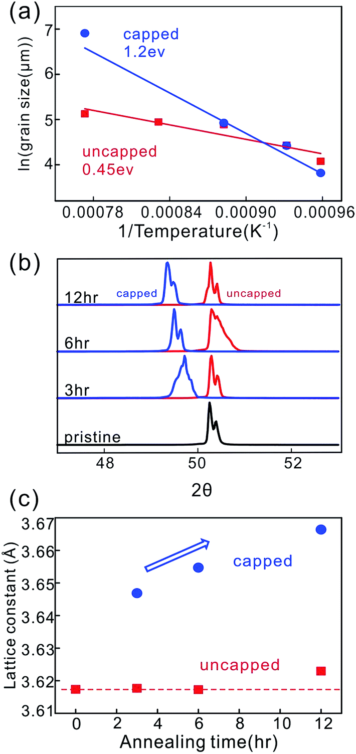 | ||
| Fig. 2 Comparison of uncapped and capped annealing conditions: (a) Arrhenius plot of grain size (b) overlay of XRD spectra evolution during annealing, (c) extracted lattice spacing vs. annealing time. | ||
The activation energy was then extracted from the Arrhenius equation according to
We find that the activation energy of grain growth for uncapped copper foil (0.45 eV) is significantly lower than capped copper foil (1.2 eV). The value of the capped case is close to the values for bulk copper.24 A lower activation energy had been previously associated with strain due to grain boundaries.24 These results suggest that uncapped copper foil exhibits a significantly higher strain whereas capped annealing results in the lowering of film strain due to recrystallization.
X-ray diffraction (XRD) was carried out to elucidate the presence of strain in the Cu lattice. The main XRD peak associated with the (200) direction exhibits a different behavior for uncapped and capped Cu foil (Fig. 2(b)). The lattice spacing was extracted from the XRD peak position and we find that the lattice constant is increasing with time for capped Cu foil but remains constant for uncapped Cu (Fig. 2(c)). We therefore conclude that the presence of an interface causes a significant relaxation of the Cu that can reach 1.3% after 12 h annealing.
The observed significant decrease of lattice strain during recrystallization could also explain the occurrence of different crystal textures after annealing. We observe that a majority of uncapped Cu annealed at various times will retain its 100 direction (Fig. 1(a)). This is expected since the foil's low thickness compared to the grain dimension causes significant interfacial stresses which promote the 100 texture to be the lowest energy state.25
Conversely, annealing with a cap was found to increase the chance of producing 111 textures (Fig. 3(a)) which is the lowest energy state of an infinite Cu crystal.26–28 This observation is important because growth on 111 textures is expected to produce higher quality graphene2 but was previously only achieved on expensive single-crystalline substrates.
 | ||
| Fig. 3 (a) EBSD images of 3 representative samples that were subjected to 8 hour capped annealing under identical conditions and their position in the color legend, (b) representative AFM images after 8 h annealing for uncapped (left) and capped Cu (right) (c) average XRD Cu (200) peak position vs. Cu roughness. | ||
We furthermore note that capped annealing can also produce large areas of exotic textures, such has 121 and 102 (Fig. 3(a)), which shows the potential of our approach for engineering the atomic orientation of metal substrates.
An improved strain relaxation is expected to significantly affect the morphology of the Cu surface. Theoretical studies found a linear relation between strain and surface roughness due to elastic deformation and predicted an increase of this effect with larger grain sizes.29
Atomic force micrographs indeed show a smoother surface for relaxed samples after capped annealing compared to strained samples after uncapped annealing (Fig. 3(b)). This result confirms the formation of an effective interface between cap and sample.
Moreover, we observe a direct correlation between the XRD peak position of copper and its roughness (Fig. 3(c)) which supports our model that strain is the controlling factor for the Cu roughness. This result highlights the potential of strain relaxation to reduce the roughness of the substrate.
The here presented ability to control the Cu morphology was subsequently applied enhance the performance of graphene films grown on it.
For this purpose Cu was first annealed in the described capped or uncapped conditions. All of the thus produced Cu foils were then subjected to CVD at the same time to limit the sample-to-sample variation. CVD for all samples was carried out using enclosure growth as reported previously.21
We observe that graphene grown on relaxed Cu foil shows a lower grain density and an increased grain size compared to Cu foil after uncapped annealing (Fig. 4(a)). This change is ascribed to a lower roughness of relaxed Cu that results in a decreasing concentration of suitable protrusions which can act as nucleation seeds.30 Additionally, the increased grain size results in a lower density of grain boundaries which have been associated with structural defects in the graphene lattice.31 Indeed Raman analysis shows a lower defectiveness of graphene grown on cap-annealed Cu as indicated by a lower average ID/IG ratio (Fig. 4(b))32 (for detailed characterization of graphene grown on cap annealed or uncapped Cu foil refer to ESI Fig. S2†). This result was confirmed by FIFE analysis33 which shows a higher coverage for capped Cu annealing (ESI Fig. S3†).
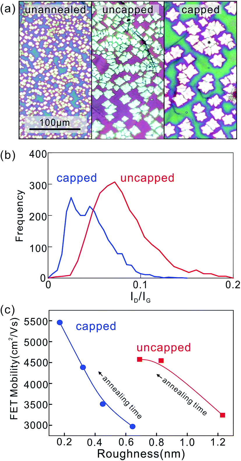 | ||
| Fig. 4 (a) Representative OM images of graphene grown on differently annealed Cu foil, (b) histograms of Raman ID/IG ratio for graphene grown on Cu foil after capped/uncapped annealing, (c) graphene FET mobility vs. roughness for capped and uncapped Cu foil after different annealing durations. | ||
Finally, the carrier mobility of graphene grown on differently annealed Cu foils was investigated (Fig. 4(c)). We find a clear trend of an improvement of mobility with annealing duration which corroborates the importance of an improved catalyst morphology. Furthermore graphene grown on 12 h cap-annealed Cu exhibited an increase in average mobility of 25% which illustrates the potential of our approach.
Conclusions
In conclusion, we have found that capped annealing can help decreasing the interfacial stress of copper foil. This effect enhances its grain growth rate and lowers the crystalline strain as confirmed by EBSD and XRD. Capped annealing was shown to reduce the roughness of copper which helps to grow graphene in high quality.Acknowledgements
YP Hsieh and M. Hofmann acknowledge financial support from Applied Materials, Inc., the Ministry of Science and Technology, and the Industrial Technology Research Institute of Taiwan.References
- K. S. Novoselov, V. I. Falko, L. Colombo, P. R. Gellert, M. G. Schwab and K. Kim, Nature, 2012, 490, 192–200 CrossRef CAS PubMed.
- Y. Ogawa, B. Hu, C. M. Orofeo, M. Tsuji, K.-i. Ikeda, S. Mizuno, H. Hibino and H. Ago, J. Phys. Chem. Lett., 2012, 3, 219–226 CrossRef CAS.
- J. D. Wood, S. W. Schmucker, A. S. Lyons, E. Pop and J. W. Lyding, Nano Lett., 2011, 11, 4547–4554 CrossRef CAS PubMed.
- L. Zhao, K. T. Rim, H. Zhou, R. He, T. F. Heinz, A. Pinczuk, G. W. Flynn and A. N. Pasupathy, Solid State Commun., 2011, 151, 509–513 CrossRef CAS.
- A. T. Murdock, A. Koos, T. B. Britton, L. Houben, T. Batten, T. Zhang, A. J. Wilkinson, R. E. Dunin-Borkowski, C. E. Lekka and N. Grobert, ACS Nano, 2013, 7, 1351–1359 CrossRef CAS PubMed.
- H. Wang, G. Wang, P. Bao, S. Yang, W. Zhu, X. Xie and W.-J. Zhang, J. Am. Chem. Soc., 2012, 134, 3627–3630 CrossRef CAS PubMed.
- Z. Yan, J. Lin, Z. Peng, Z. Sun, Y. Zhu, L. Li, C. Xiang, E. L. Samuel, C. Kittrell and J. M. Tour, ACS Nano, 2012, 6, 9110–9117 CrossRef CAS PubMed.
- Y. A. Wu, Y. Fan, S. Speller, G. L. Creeth, J. T. Sadowski, K. He, A. W. Robertson, C. S. Allen and J. H. Warner, ACS Nano, 2012, 6, 5010–5017 CrossRef CAS PubMed.
- D. Geng, B. Wu, Y. Guo, L. Huang, Y. Xue, J. Chen, G. Yu, L. Jiang, W. Hu and Y. Liu, Proc. Natl. Acad. Sci. U. S. A., 2012, 109, 7992–7996 CrossRef CAS PubMed.
- P. Y. Huang, C. S. Ruiz-Vargas, A. M. van der Zande, W. S. Whitney, M. P. Levendorf, J. W. Kevek, S. Garg, J. S. Alden, C. J. Hustedt, Y. Zhu, J. Park, P. L. McEuen and D. A. Muller, Nature, 2011, 469, 389–392 CrossRef CAS PubMed.
- H. Ago, Y. Ogawa, M. Tsuji, S. Mizuno and H. Hibino, J. Phys. Chem. Lett., 2012, 3, 2228–2236 CrossRef CAS PubMed.
- Q. Yu, L. A. Jauregui, W. Wu, R. Colby, J. Tian, Z. Su, H. Cao, Z. Liu, D. Pandey, D. Wei, T. F. Chung, P. Peng, N. P. Guisinger, E. A. Stach, J. Bao, S.-S. Pei and Y. P. Chen, Nat. Mater., 2011, 10, 443–449 CrossRef CAS PubMed.
- M. D. S. Lakshad Wimalananda, J.-K. Kim and J.-M. Lee, Carbon, 2016, 108, 127–134 CrossRef CAS.
- K. P. Sharma, S. M. Shinde, M. S. Rosmi, S. Sharma, G. Kalita and M. Tanemura, J. Mater. Sci., 2016, 51, 7220–7228 CrossRef CAS.
- L. Brown, E. B. Lochocki, J. Avila, C.-J. Kim, Y. Ogawa, R. W. Havener, D.-K. Kim, E. J. Monkman, D. E. Shai and H. I. Wei, Nano Lett., 2014, 14, 5706–5711 CrossRef CAS PubMed.
- L. Lu, M. Sui and K. Lu, Acta Mater., 2001, 49, 4127–4134 CrossRef CAS.
- G. K. Williamson and R. E. Smallman, Philos. Mag., 1956, 1, 34–46 CrossRef CAS.
- S. Schmidt, S. F. Nielsen, C. Gundlach, L. Margulies, X. Huang and D. J. Jensen, Science, 2004, 305, 229–232 CrossRef CAS PubMed.
- R. E. Reed-Hill and R. Abbaschian, Physical metallurgy principles, 1973 Search PubMed.
- A. Vattré, T. Jourdan, H. Ding, M. C. Marinica and M. J. Demkowicz, Nat. Commun., 2016, 7, 10424 CrossRef PubMed.
- Y. P. Hsieh, Y. J. Chiu and M. Hofmann, Nanoscale, 2015, 7, 19403–19407 RSC.
- D. Nezich, A. Reina and J. Kong, Nanotechnology, 2011, 23, 015701 CrossRef PubMed.
- D. L. Duong, G. H. Han, S. M. Lee, F. Gunes, E. S. Kim, S. T. Kim, H. Kim, Q. H. Ta, K. P. So and S. J. Yoon, Nature, 2012, 490, 235–239 CrossRef CAS PubMed.
- S. K. Ganapathi, D. M. Owen and A. H. Chokshi, Scr. Metall. Mater., 1991, 25, 2699–2704 CrossRef.
- N. J. Park, D. P. Field, M. M. Nowell and P. R. Besser, J. Electron. Mater., 2005, 34, 1500–1508 CrossRef CAS.
- C. V. Thompson and R. Carel, J. Mech. Phys. Solids, 1996, 44, 657–673 CrossRef CAS.
- J. M. E. Harper, C. Cabral, P. C. Andricacos, L. Gignac, I. C. Noyan, K. P. Rodbell and C. K. Hu, J. Appl. Phys., 1999, 86, 2516 CrossRef CAS.
- S.-C. Chang, J.-M. Shieh, B.-T. Dai, M.-S. Feng and Y.-H. Li, J. Electrochem. Soc., 2002, 149, G535 CrossRef CAS.
- A. Perron, I. O. Politano and V. Vignal, Grain size, stress and surface roughness, Wiley, Chichester, ROYAUME-UNI, 2008 Search PubMed.
- H. Ya-Ping, C. Yi-Hung, T. He-Guang and H. Mario, Nanotechnology, 2016, 27, 105602 CrossRef PubMed.
- H. Zhou, W. J. Yu, L. Liu, R. Cheng, Y. Chen, X. Huang, Y. Liu, Y. Wang, Y. Huang and X. Duan, Nat. Commun., 2013, 4, 2096 Search PubMed.
- M. S. Dresselhaus, A. Jorio, M. Hofmann, G. Dresselhaus and R. Saito, Nano Lett., 2010, 10, 751–758 CrossRef CAS PubMed.
- M. Hofmann, Y. C. Shin, Y.-P. Hsieh, M. S. Dresselhaus and J. Kong, Nano Res., 2012, 5, 504–511 CrossRef CAS.
Footnote |
| † Electronic supplementary information (ESI) available: Detailed characterization of Cu foil, graphene quality and continuity. See DOI: 10.1039/c6ra25750j |
| This journal is © The Royal Society of Chemistry 2017 |