
 Open Access Article
 This Open Access Article is licensed under a
 Creative Commons Attribution 3.0 Unported Licence
Photoluminescence and electrical properties of bidirectional ZnO nanowires on Zn foils via a thermal oxidation method
Zhang-Wei Wua,
Shing-Long Tyan *ab,
Hsin-Hsien Chenb,
Jung-Chun-Andrew Huangab,
Chung-Lin Wub,
Chia-Roong Leea and
Ting-Shan Moc
*ab,
Hsin-Hsien Chenb,
Jung-Chun-Andrew Huangab,
Chung-Lin Wub,
Chia-Roong Leea and
Ting-Shan Moc
aDepartment of Photonics, National Cheng Kung University, Tainan, Taiwan 701, Taiwan. E-mail: sltyan@mail.ncku.edu.tw
bDepartment of Physics, National Cheng Kung University, Tainan, Taiwan 701, Taiwan
cDepartment of Electronic Engineering, Kun Shan University of Technology, Tainan, Taiwan 710, Taiwan
First published on 17th January 2017
Abstract
ZnO nanowires (NWs) were directly grown on ductile zinc foils through a two-step process: (a) large, thin, and ductile Zn foils were fabricated from a mixture of Zn and ZnO powders; and (b) ZnO NWs were produced by thermal oxidation at temperatures of 300–600 °C. The ZnO NWs presented preferential growth in the [101] orientation. The highly crystalline NWs synthesized at 500 °C exhibited a bidirectional mode with an angle of approximately 60° between their longitudinal axes. On foils oxidized at 600 °C, the NWs evolved into nanotowers. The photoluminescence (PL) spectra showed strong peaks at approximately 368 nm and weaker peaks at approximately 374 nm in the UV region; moreover, a broad deep-level-related green emission peak was recorded at approximately 520 nm in the visible region. The PL green emission line was strongly suppressed for the samples produced at higher oxidation temperatures, which indicated good optical qualities. These good optical qualities, combined with the bidirectional mode and the ductility of the foil, are expected to be useful for flexible planar device applications. The electrical properties of a single ZnO NW were investigated. I–V measurements revealed the Schottky characteristics of the NWs and the resistivity of the ZnO NWs was measured to be ∼93 Ω cm.
1. Introduction
Over the past two decades, one-dimensional nanostructured materials have received increasing attention in various fields of nanotechnology because of their unique physical and chemical properties. Among these materials, ZnO NWs have been one of the most investigated because of their superior electrical,1,2 mechanical,3,4 and optical properties.5,6 Currently, substantial effort has been devoted to the fabrication of ZnO NW-based flexible devices. Commonly used flexible substrates can be grouped into two main categories, metal sheets and plastic substrates. In the case of plastic substrate, integration of NWs is limited by the necessity of a seed layer,7,8 poor adhesion of nanostructures on the underlying substrate and/or thermal degradation of the plastic during high-temperature processing. In the contrary, most applications of NW arrays often require their assembly on conductive surfaces for electrical addressing, control, and detection. The integration of metal substrates for ZnO NWs has been widely studied, including brass,9 steel alloy,10 FeCrAl metal alloy,11 Zn foil,12–20 etc. Among these metal substrates, Zn foil is considered as a promising material because it can act as both a reactant and flexible substrate, thus, the synthesis and assembly of ZnO NWs can be accomplished in one step, and the naturally good adhesion or electrical connection between the ZnO NWs and the conductive substrate can be realized.The initial zinc morphology plays a decisive role in the subsequent NWs growth.21 Typically, Zn foils used for ZnO NWs fabrication were supplied commercially13–15,18–20 and the surface morphologies of all foils used in the fabrication should be similar to each other. Therefore, homemade Zn foils with different Zn morphology are increasingly preferred and necessary.
A favorable technique integration of ZnO NWs is based on a solution method,18–20,22–28 however, it suffers from long reaction time, high degree of reaction parameter control and the poor quality of NWs. Moreover, ZnO NWs have been synthesized by thermal evaporation,12,13 vapor transport,11,29–32 and thermal oxidation methods.14–17 The thermal evaporation method requires a type of complex process control that is unfavorable for an industrialized process. A pseudobuffer layer must improve interface properties before NWs can be grown using the vapor transport method. Compared to these methods, noncatalytic thermal oxidation technique has been considered powerful and attractive because of its simplicity, high yield, and low cost. However, few reports have described ZnO NWs grown directly on homemade Zn foil by thermal oxidation techniques.
Bridged nanostructure is an important configuration in planar-type devices. The bridging NWs grow on two electrodes and contact together to form wire–wire junction and act as sensing probes.33,34 However, most the ZnO NWs grown on Zn foil by thermal oxidation technique are randomly dispersed on the foil14–17 and inadequate to fabricate the planar nanodevices. A feasible method is to grow ZnO NWs on the facets of Zn crystal hexagonal structures because it can increase the probabilities of wire–wire junctions in horizontal direction compared to the randomly radial NWs.
Motivated by the aforementioned speculations and problems, in this study, we report the synthesis of ZnO NWs grown directly on Zn foil using a two-step process: (a) Zn foil fabrication; and (b) ZnO NWs synthesized by thermal oxidation at temperatures of 300–600 °C. Effect of the oxidation temperature on PL spectra and structural properties of ZnO NWs is studied. The electrical properties of the NWs are investigated using a two-terminal NW device.
2. Experiment
Mensah et al.35 reported that a site located at a step edge for a growth surface with a step can generate a higher probability of nuclei formation. In order to prepare the Zn foil with a maximized number of step edges and to prevent the molten Zn from agglomerating, Zn (99.99%) and ZnO (99.7%) powders (1![[thin space (1/6-em)]](https://www.rsc.org/images/entities/char_2009.gif) :1 in weight ratio) were thoroughly mixed and pressed into sheets 7.5 cm in diameter and 3 mm thick. The sheets were then bombarded for 1.5 h in an argon plasma reactor equipped with a 150 W power supply. The chamber pressure just before heating was 1 × 10⁻⁵ Torr. After the system had cooled naturally to room temperature, large, thin Zn foils were obtained. The second step is the thermal oxidation process. Prior to oxide, the Zn foils were cut into 1 × 1 cm2 pieces, then ultrasonically cleaned in acetone for 10 min, and then in isopropanol for 10 min, rinsed in deionized water for 10 min in each step, and dried by blowing nitrogen gas onto them. The cleaned specimens were progressed with direct furnace thermal oxidation in an oxygen ambience. A flow of high-purity oxygen (99.99%) was first introduced into the quartz tube at a high rate (approximately 30 sccm) for 30 min to remove air in the system, and the flow was then adjusted to 20 sccm. At this time, the tube furnace was heated to 300 °C, 400 °C, 500 °C, and 600 °C. After being held at this temperature for 15 min, the system was allowed to cool naturally to room temperature under a continuing flow of oxygen gas. The product samples were then collected, and a gray layer was observed on the surfaces of the samples.
:1 in weight ratio) were thoroughly mixed and pressed into sheets 7.5 cm in diameter and 3 mm thick. The sheets were then bombarded for 1.5 h in an argon plasma reactor equipped with a 150 W power supply. The chamber pressure just before heating was 1 × 10⁻⁵ Torr. After the system had cooled naturally to room temperature, large, thin Zn foils were obtained. The second step is the thermal oxidation process. Prior to oxide, the Zn foils were cut into 1 × 1 cm2 pieces, then ultrasonically cleaned in acetone for 10 min, and then in isopropanol for 10 min, rinsed in deionized water for 10 min in each step, and dried by blowing nitrogen gas onto them. The cleaned specimens were progressed with direct furnace thermal oxidation in an oxygen ambience. A flow of high-purity oxygen (99.99%) was first introduced into the quartz tube at a high rate (approximately 30 sccm) for 30 min to remove air in the system, and the flow was then adjusted to 20 sccm. At this time, the tube furnace was heated to 300 °C, 400 °C, 500 °C, and 600 °C. After being held at this temperature for 15 min, the system was allowed to cool naturally to room temperature under a continuing flow of oxygen gas. The product samples were then collected, and a gray layer was observed on the surfaces of the samples.
The crystallinity of the NWs and the orientation of growth were investigated by grazing incidence X-ray diffraction (GIXRD). An exhaustive structural characterization of the NWs were carried out by high-resolution scanning transmission electron microscopy (HRSTEM, JEOL JEM-2100F) with a selected area electron diffraction (SAED) pattern and energy dispersive X-ray (EDX) spectrometry. The surface morphologies were investigated by scanning electron microscopy (SEM, Zeiss Supra-55). Photoluminescence (PL) spectra were performed (Jobin-Yvon TRIAX 550) at a low temperature (20 K) for optical investigation, using a He–Cd laser (325 nm) as the excitation source. The electrical property of a single ZnO NW was investigated by two-point probe I–V measurement. A single NW was transferred onto an undoped Si substrate with a 200 nm-thick SiO2 layer, and a focused ion beam (FIB, FEI Nova-200) was employed to make electrodes at the NW end. Platinum was selected as the electrode material. Electrical measurements were performed in an ambient environment at room temperature in air and under dark conditions. A Keithley 2400 picoammeter and voltage–current source were used under computer control.
3. Results and discussion
Fig. 1(a) shows a photograph of the as-grown Zn foil. It reveals that the foil is approximately 5 cm in diameter and approximately 0.1 mm in thickness. It is bendable (the inset of Fig. 1(a)), and can be cut or torn easily. This ductile foil can easily be formed into various geometrical shapes, such as U-, S-, and roller shapes. This ductile property is expected to be useful for flexible device applications. The SEM images of surface morphology for different zones are shown in Fig. 1(b)–(f). These images illustrated the surface uniformity of the foil. In each region, the Zn grains formed on the foil surface on a scale of several tens of microns and had laminated structures with hexagonal-shaped ends and step side faces. The development of the laminar structures was caused by the impurities in the commercially 4 N purity zinc powder, such as lead, bismuth, cadmium and iron.36 In our case, the levels of contaminants were below 5 ppm. The laminated structures indicated that the growth mode of the Zn grains was layer-by-layer growth. In addition, most grain axes tended to be aligned in the foil plane.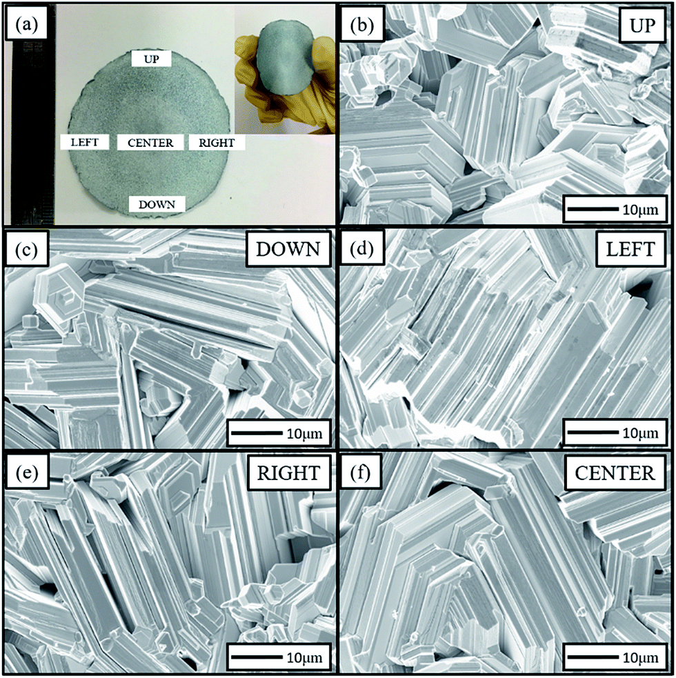 | ||
| Fig. 1 Zn foil and the surface morphologies of different zones; (a) the flexibility of the Zn foil; (b)–(f) SEM images of the different zones of the Zn foil. | ||
Fig. 2 presents the typical SEM images of the Zn foils oxidized at temperatures ranging from 300 °C to 600 °C. For the sample oxidized at 300 °C, ZnO nanoclusters and sparse NWs were observable on the step side faces, as shown in Fig. 2(a), the inset of Fig. 2(a) shows the sizes of ZnO nanoclusters were 200–300 nm; the lengths of the NWs were less than 1 μm. For the sample prepared at an oxidization temperature of 400 °C, as shown in Fig. 2(b), ZnO NWs became longer (1–5 μm). Fig. 2(c) shows the dense ZnO NWs (∼13 μm−2) that formed on the sample prepared at an oxidation temperature of 500 °C. It is worth noting that ZnO NWs, as shown in the inset, were generated in two directions. The two sets of NWs had an angle of approximately 60° between them. The bidirectional growth mode of the ZnO NWs differed from the conventional common growth mode, with one preferential growth direction, observed in most syntheses of ZnO NWs on Zn foils.37–39 The growth of ZnO NWs on m-plane sapphire substrates with a longitudinal axis making an angle of 60° with the substrate has been reported.35,40,41 However, to the best of our knowledge, the bidirectional growth of ZnO NWs with an intersection angle of approximately 60° on Zn foil has never observed. The bidirectional growth of the NWs indicates the NWs are not randomly oriented but highly oriented. The observation of separated and parallel NWs indicates that the alignment of NWs was caused by epitaxial growth.42 The vast majority of NWs evolved into nanotowers with a density of ∼0.3 μm−2 for the sample prepared at an oxidation temperature of 600 °C, as shown in Fig. 2(d). The inset shows the enlarged shape of a nanotower; similar ZnO nanostructures have also been reported.27
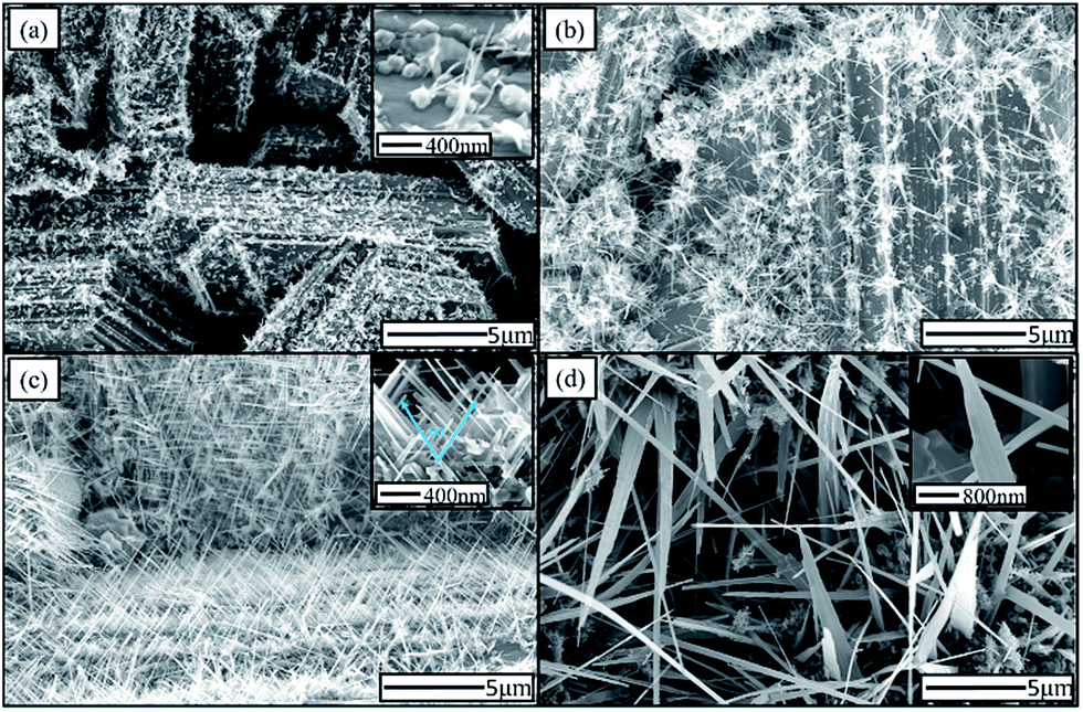 | ||
| Fig. 2 SEM images of samples oxidized at (a) 300 °C, (b) 400 °C, (c) 500 °C, and (d) 600 °C. | ||
The crystal structures of the as-grown Zn foil and samples oxidized at temperatures ranging from 300 °C to 600 °C were investigated by the GIXRD. Fig. 3(a) shows the GIXRD pattern of the as-grown Zn foil. Metallic Zn with the (100), (101), (102), (103), and (110) diffraction lines was observed (JCPDS card no. 04-0831). Clearly, the as-grown Zn foil is a hexagonal close-packed crystal structure. Fig. 3(b)–(e) show the GIXRD patterns of the foils oxidized at 300, 400, 500, and 600 °C, respectively. Each spectrum shows a mixed pattern of Zn and ZnO peaks (JCPDS card no. 36-1451), except spectrum (e). As the sample oxidized at 300 °C, an additional weak ZnO (101) line except Zn peaks is found and the intensity of the Zn peaks change slightly, indicating that only a small amount of Zn had transformed to ZnO. From SEM image of Fig. 2(a) we know that sparse ZnO NWs had just formed, which caused the low intensity of the diffraction peak. For the samples oxidized above 400 °C, ZnO diffraction lines corresponding to a hexagonal wurtzite crystal structure were observed. The intensities of ZnO peaks of the sample annealed at 500 °C were stronger than those obtained from the sample annealed at 400 °C because denser NWs formed. The intensity of Zn peak (101) was dramatically lower for the sample oxidized at 500 °C, which indicates more Zn had transformed to ZnO NWs. These XRD patterns indicated the NWs were preferentially oriented in [101] direction. For the sample prepared at an oxidization temperature of 600 °C, only ZnO peaks were observed; the Zn peaks had completely disappeared. From the SEM image shown in Fig. 2(d), it can be seen that the vast majority of NWs evolved into nanotowers, therefore, Zn signals were highly suppressed. The XRD peaks corresponding to Zn in Fig. 2(b)–(d) could be attributed to the uncovered portion of the zinc foil,12 the disappearance of the Zn peaks indicates the Zn was converted to ZnO nanotowers combined with the transformation of Zn into ZnO in the uncovered areas.
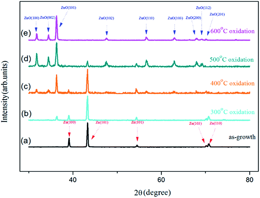 | ||
| Fig. 3 GIXRD spectra of (a) as-grown sample and samples oxidized at (b) 300 °C, (c) 400 °C, (d) 500 °C, and (e) 600 °C. | ||
Detailed structural characterization of the grown ZnO NWs was performed using TEM combined with an SAED pattern. A typical TEM image of ZnO NWs obtained from a sample oxidized at a temperature of 500 °C is shown in Fig. 4(a). The widths of ZnO NWs were 20–140 nm. Fig. 4(b) shows the HRSTEM image of a single NW and its Fourier filtered image is shown in the inset. From the HRSTEM image, the NWs are highly crystalline with a lattice spacing of 0.25 nm, which corresponds to the d-spacing of (10![[1 with combining macron]](https://www.rsc.org/images/entities/char_0031_0304.gif) 1) crystal planes of wurtzite ZnO. In addition, no stacking fault was found, indicating that the ZnO NWs had low defect concentrations. The result of SAED pattern shown in Fig. 4(c) is consistent with the HRSTEM image and indicates that the ZnO NWs grew along [101] direction. The EDS spectrum in Fig. 4(d) reveals that the atom composition ratio in ZnO NWs was close to 1:1; it also provides evidence that the ZnO NWs were highly crystalline.
1) crystal planes of wurtzite ZnO. In addition, no stacking fault was found, indicating that the ZnO NWs had low defect concentrations. The result of SAED pattern shown in Fig. 4(c) is consistent with the HRSTEM image and indicates that the ZnO NWs grew along [101] direction. The EDS spectrum in Fig. 4(d) reveals that the atom composition ratio in ZnO NWs was close to 1:1; it also provides evidence that the ZnO NWs were highly crystalline.
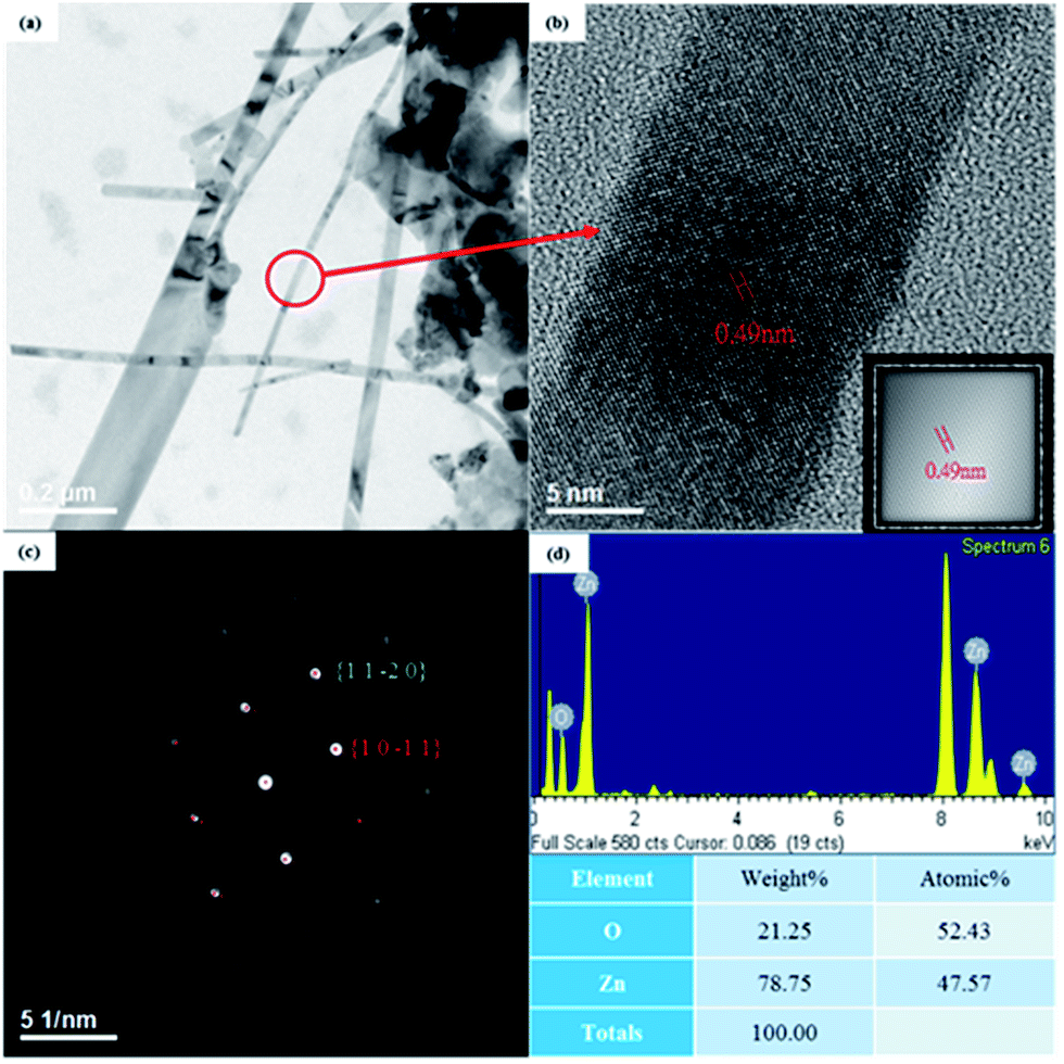 | ||
| Fig. 4 (a) TEM image with low magnification and (b) a high-resolution image of a ZnO nanowire (inset is the Fourier filtered image). (c) SAED pattern and (d) EDS spectrum. | ||
The growth process of ZnO NWs in our synthetic process can be explained on the basis of reactant species and the crystallographic habits of wurtzite hexagonal ZnO. Fig. 5(a) shows a Zn grain. One of the uneven profiles of the step side faces is shown in Fig. 5(b). When the oxidation temperature was 300 °C, Zn and O atoms reacted to form ZnO nanoclusters, as shown in Fig. 5(c). The nanoclusters preferred to condense at the step edges.35 In our synthetic process, the step side faces offered higher probabilities for nanocluster formation and promoted the formation of the final products. With increased temperature (Fig. 5(d)), ZnO had a preferred orientation along the (101) plane. This crystal plane was related to the oxidation rate, which led to inclusion of absorbed oxygen atoms in the ZnO lattice.43,44 Therefore, for samples prepared at a higher oxidation temperature, the ZnO presented preferential growth in the [101] orientation. Finally, ZnO NWs broadened and lengthened to form nanotowers at 600 °C, as shown in Fig. 5(e). Fig. 5(f) shows the bidirectional growth mode of ZnO NWs with an intersection angle of 60° as viewed from the y–z plane. From the crystal structure analysis we knew both the planes made an angle of 62° with the base plane. The angle between the two planes, 56°, was in good agreement with the observed value of approximately 60°.
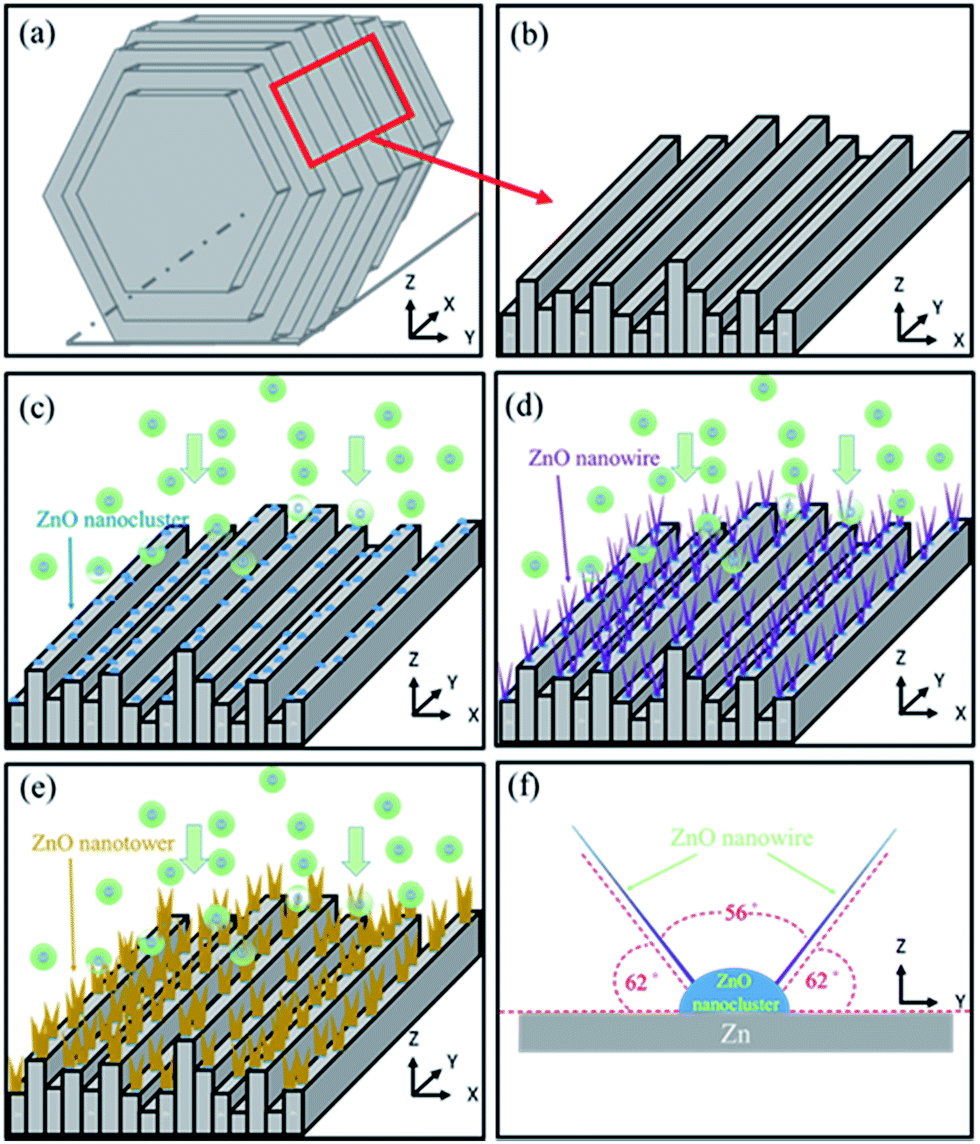 | ||
| Fig. 5 Schematic of growth process: (a) a Zn grain of laminated structure with hexagonal-shaped ends and step side faces. (b) A step side face of the Zn grain. (c) ZnO nanoclusters formed at step edges. (d) ZnO nanowires in a developed state. (e) ZnO nanowires evolved into nanotowers. (f) A view from the y–z plane; ZnO nanowires are generated with an angle of 56° between them. | ||
Fig. 6 shows the low temperature PL spectra in the wavelength range of 360–600 nm for the Zn foils annealed at different temperatures. All spectra exhibited a dominant near-band-edge emission (NBE) peak at approximately 368 nm in the UV region, which is ascribed to the PL emission of donor-bound excitons.45,46 Apart from the dominant peak, a further peak was observed at approximately 374 nm and can be ascribed to defect related emission (DRE)47–49 and zinc vacancies (VZn) located in the vicinity of the surface corresponding to the defect.49 In the visible region, a spectrally broad deep-level-related green emission (DLE) peak at approximately 520 nm that originated from oxygen vacancies (VO)39,50,51 was observed only in spectra (a) and (b).
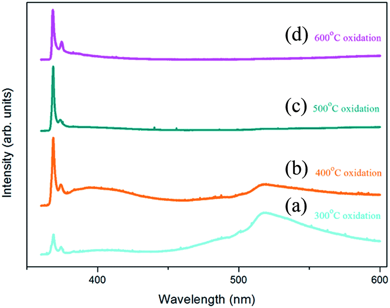 | ||
| Fig. 6 PL spectra of samples oxidized at (a) 300 °C, (b) 400 °C, (c) 500 °C, and (d) 600 °C. | ||
In spectrum (a), the 300 °C oxidized sample showed low-intensity PL signals because of sparse ZnO NWs. In spectrum (b), for the sample prepared at an oxidation temperature of 400 °C, the PL peak intensities increase because of the greater number of NWs involved in the luminescence process. It is worth noting that the relative PL intensity ratio of the DLE to the NBE emission (IDLE/INBE) changed obviously as compared with that obtained from spectrum (a). The ratio gives relevant information regarding the concentration of structural defects.52,53 The values of IDLE/INBE obtained from spectra (b) and (a) were 0.347 and 1.983 respectively. The lower value indicated that the lower defect concentration in the NWs formed at an oxidation temperature of 400 °C. For the sample oxidized at 500 °C [spectrum (c)], the DLE peak was highly suppressed, indicating very low defect concentrations. This was inconsistent with the result of HRSTEM analysis [Fig. 4(b)], which showed the ZnO NWs to be highly crystalline. Spectrum (d) showed the PL signal obtained for the sample oxidized at 600 °C. Similar to that of spectrum (c), the DLE peak disappeared and only the peaks in the UV region survived. The relative DRE peak intensity was high because of the increased defects in the vicinity of the wider nanotowers, which had large surfaces.
A cross-sectional schematic diagram of two-terminal NW device for ZnO NW transport measurement is shown in Fig. 7(a). The silicon substrate was capped with a 200 nm-thick SiO2 layer. The ZnO NWs synthesized at 500 °C were then randomly dispersed on the substrate and positioned using SEM. A Pt layer (500 nm) was deposited using standard FIB. The top view SEM image is shown in Fig. 7(b). The I–V curve was obtained by sweeping the voltage from −5 to 5 V and recording the electrical current simultaneously; its result is shown in Fig. 7(c). The I–V curve exhibited rectifying characteristics and the nonlinear nature was typical of Schottky contact for the metal–semiconductor junction. The resistivity of the Pt leads was approximately 5 × 10⁻⁴ Ω cm for the FIB deposited Pt film, therefore we neglected electrode resistance in our electrical measurement. The resistivity, ρ ∼ 93 Ω cm, was calculated from measuring the resistance R (slope of the linear I–V curve) and using the relationship ρ = A/RL, where R is the resistance, L the NW length, and A is the cross section of the ZnO NW. The resistivity is approximately two orders of magnitude greater than that of ZnO NWs grown by anodizing Zn foil.42,54 This indicates its high quality, which has been further confirmed by our observation of a strong UV emission at ∼368 nm and a very weak green band from the PL spectrum shown in Fig. 6(c). This electrical measurement of our NWs supports the degree of electrical quality achievable in NWs synthesized by our method.
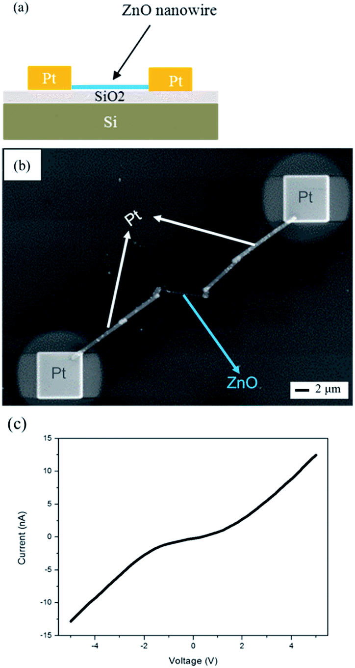 | ||
| Fig. 7 (a) Schematic diagram and (b) SEM image of structure for transport measurements of a single nanowire. (c) I–V curve of the ZnO nanowire. | ||
4. Conclusions
In conclusion, large quantities of ZnO NWs and nanotowers have been synthesized on flexible Zn substrates by thermal oxidation processes at 500 °C and 600 °C, respectively. XRD, HRSTEM, and SAED results showed that ZnO NWs were highly crystalline and preferentially oriented along the (101) plane. In addition, the ZnO NWs showed a bidirectional growth mode and the angle between the two directions was approximately 60°. I–V measurement revealed Schottky characteristics of the NWs and the resistivity was approximately 93 Ω cm. The PL spectrum of the ZnO NWs revealed good optical qualities, suggesting their suitability for use in the fabrication of flexible planar UV detectors and gas sensors.Acknowledgements
This research received funding from the Headquarters of University Advancement at the National Cheng Kung University, which is sponsored by the Ministry of Education, Taiwan, ROC. The authors would like to thank the Center for Micro/Nano Science and Technology, National Cheng Kung University, Tainan, Taiwan, for access to equipment and technical support. We also thank J. X. Huang, Y. C. Lin, Y. C. Huang and H. F. Liu for their help in experiments.References
- W.-K. Hong, B.-J. Kim, T.-W. Kim, G. Jo, S. Song, S.-S. Kwon, A. Yoon, E. A. Stach and T. Lee, Colloids Surf., A, 2008, 313–314, 378–382 CrossRef.
- S. Song, W.-K. Hong, S.-S. Kwon and T. Lee, Appl. Phys. Lett., 2008, 92, 263109 CrossRef.
- C. Q. Chen and J. Zhu, Appl. Phys. Lett., 2007, 90, 043105 CrossRef.
- B. M. Wen, Y. Z. Huang and J. J. Boland, J. Phys. Chem. C, 2008, 112, 106–111 CAS.
- Y. Wang, Z. Liao, G. She, L. Mu, D. Chen and W. Shi, Appl. Phys. Lett., 2011, 98, 203108 CrossRef.
- Y.-R. Li, C.-Y. Wan, C.-T. Chang, W.-L. Tsai, Y.-C. Huang, K.-Y. Wang, P.-Y. Yang and H.-C. Cheng, Vacuum, 2015, 118, 48–54 CrossRef CAS.
- C. M. García, E. D. Valdés, A. M. P. Mercado, A. F. Méndez Sánchez, J. A. Andraca Adame, V. Subramaniam and J. R. Ibarra, Adv. Mater. Phys. Chem., 2012, 02, 4 Search PubMed.
- J. Liu, W. Wu, S. Bai and Y. Qin, ACS Appl. Mater. Interfaces, 2011, 3, 4197–4200 CAS.
- X. Wang, K. Huo, F. Zhang, Z. Hu, P. K. Chu, H. Tao, Q. Wu, Y. Hu and J. Zhu, J. Phys. Chem. C, 2009, 113, 170–173 CAS.
- A. Umar, J.-P. Jeong, E.-K. Suh and Y.-B. Hahn, Korean J. Chem. Eng., 2006, 23, 860–865 CrossRef CAS.
- N.-D. Tam, S. Karandeep, M. Meyyappan and M. O. Michael, Nanotechnology, 2012, 23, 194015 CrossRef PubMed.
- G. Tandra, B. Subhajit, K. Soumitra, D. Apurba, C. Supriya and C. Subhadra, Nanotechnology, 2008, 19, 065606 CrossRef PubMed.
- E. Mosquera, J. Bernal, M. Morel and R. A. Zarate, J. Nanoeng. Nanomanuf., 2012, 2, 253–258 CrossRef CAS.
- F. J. Sheini, D. S. Joag and M. A. More, International Scholarly and Scientific Research & Innovation, 2011, 5, 109 Search PubMed.
- L. Yuan, C. Wang, R. Cai, Y. Wang and G. Zhou, J. Cryst. Growth, 2014, 390, 101–108 CrossRef CAS.
- W. K. Tan, K. A. Razak, K. Ibrahim and Z. Lockman, J. Alloys Compd., 2011, 509, 6806–6811 CrossRef CAS.
- S. Himanshu, T. Pragya, A. K. Srivastava, P. Sanjay and S. K. Deb, Semicond. Sci. Technol., 2011, 26, 085030 CrossRef.
- J.-Y. Kim, H. Jeong and D.-J. Jang, J. Nanopart. Res., 2011, 13, 6699 CrossRef CAS.
- X. Fen, Y. Zhong-Yong, D. Gao-Hui, R. Tie-Zhen, B. Claire, H. Matej and S. Bao-Lian, Nanotechnology, 2006, 17, 588 CrossRef.
- G. H. Du, F. Xu, Z. Y. Yuan and G. V. Tendeloo, Appl. Phys. Lett., 2006, 88, 243101 CrossRef.
- C. X. Zhao, Y. F. Li, J. Zhou, L. Y. Li, S. Z. Deng, N. S. Xu and J. Chen, Cryst. Growth Des., 2013, 13, 2897–2905 CAS.
- B. Reeja-Jayan, E. De la Rosa, S. Sepulveda-Guzman, R. A. Rodriguez and M. J. Yacaman, J. Phys. Chem. C, 2008, 112, 240–246 CAS.
- R. Pérez-Hernández, A. Gutiérrez-Martínez, A. Mayoral, F. L. Deepak, M. E. Fernández-García, G. Mondragón-Galicia, M. Miki and M. Jose-Yacaman, Adv. Mater. Res., 2010, 132, 205–219 CrossRef.
- R. L. Pérez-Hernández, J. J. S. V. Z. Salazar and M. J. Yacaman, J. Nano Res., 2011, 14, 69–82 CrossRef.
- E. D. L. Rosa, S. S. lveda-Guzman, B. Reeja-Jayan, P. S. A. Torres, N. Elizondo and M. J. Yacaman, J. Phys. Chem. C, 2007, 111, 8489–8495 Search PubMed.
- C. Liu, Y. Masuda, Y. Wu and O. Takai, Thin Solid Films, 2006, 503, 110–114 CrossRef CAS.
- G. Muñoz-Hernández, A. Escobedo-Morales and U. Pal, Cryst. Growth Des., 2009, 9, 297–300 Search PubMed.
- G. Mondragon-Galicia, C. Gutierrez-Wing, M. Eufemia Fernandez-Garcia, D. Mendoza-Anaya and R. Perez-Hernandez, RSC Adv., 2015, 5, 42568–42571 RSC.
- J. Xiao, W. Zhang, Y. Wu and H. Sun, Cryst. Res. Technol., 2008, 43, 634–639 CrossRef CAS.
- X. Liu, X. Wu, H. Cao and R. P. H. Chang, J. Appl. Phys., 2004, 95, 3141–3147 CrossRef CAS.
- X. Wang, C. J. Summers and Z. L. Wang, Nano Lett., 2004, 4, 423–426 CrossRef CAS PubMed.
- X. Y. Kong, Y. Ding and Z. L. Wang, J. Phys. Chem. B, 2004, 108, 570–574 CrossRef CAS.
- M. R. Alenezi, S. J. Henley and S. R. P. Silva, Sci. Rep., 2015, 5, 8516 CrossRef PubMed.
- H. Nguyen, C. T. Quy, N. D. Hoa, N. T. Lam, N. V. Duy, V. V. Quang and N. V. Hieu, Sens. Actuators, B, 2014, 193, 888–894 CrossRef CAS.
- S. L. Mensah, V. K. Kayastha, I. N. Ivanov, D. B. Geohegan and Y. K. Yap, Appl. Phys. Lett., 2007, 90, 113108 CrossRef.
- M. V. Akdeniz, C. N. Reid and J. V. Wood, Mater. Sci. Eng., 1988, 98, 321 CrossRef CAS.
- D. Deng, S. T. Martin and S. Ramanathan, Nanoscale, 2010, 2, 2685–2691 RSC.
- C. Florica, N. Preda, A. Costas, I. Zgura and I. Enculescu, Mater. Lett., 2016, 170, 156–159 CrossRef CAS.
- E. Mosquera, J. Bernal, R. A. Zarate, F. Mendoza, R. S. Katiyar and G. Morell, Mater. Lett., 2013, 93, 326–329 CrossRef CAS.
- J. Zúñiga-Pérez, A. Rahm, C. Czekalla, J. Lenzner, M. Lorenz and M. Grundmann, Nanotechnology, 2007, 18, 195303 CrossRef.
- H. T. Ng, B. Chen, J. Li, J. Han, M. Meyyappan, J. Wu, S. X. Li and E. E. Haller, Appl. Phys. Lett., 2003, 82, 2023–2025 CrossRef CAS.
- S. Cho and K.-H. Lee, Cryst. Growth Des., 2010, 10, 1289 CAS.
- G.-H. Lee, Electron. Mater. Lett., 2010, 6, 155–159 CrossRef CAS.
- K. Lim, M. A. Hamid, R. Shamsudin, N. H. Al-Hardan, I. Mansor and W. Chiu, Materials, 2016, 9, 300 CrossRef.
- D. C. Look, D. C. Reynolds, C. W. Litton, R. L. Jones, D. B. Eason and G. Cantwell, Appl. Phys. Lett., 2002, 81, 1830–1832 CrossRef CAS.
- T. Matsumoto, H. Kato, K. Miyamoto, M. Sano, E. A. Zhukov and T. Yao, Appl. Phys. Lett., 2002, 81, 1231–1233 CrossRef CAS.
- V. S. Yalishev, Y. S. Kim, X. L. Deng, B. H. Park and S. U. Yuldashev, J. Appl. Phys., 2012, 112, 013528 CrossRef.
- C. Liu, H. He, L. Sun, Q. Yang, Z. Ye and L. Chen, Solid State Commun., 2010, 150, 2303–2305 CrossRef CAS.
- D. Tainoff, B. Masenelli, P. Mélinon, A. Belsky, G. Ledoux, D. Amans, C. Dujardin, N. Fedorov and P. Martin, Phys. Rev. B: Condens. Matter Mater. Phys., 2010, 81, 115304 CrossRef.
- X. Yang, G. Du, X. Wang, J. Wang, B. Liu, Y. Zhang, D. Liu, D. Liu, H. C. Ong and S. Yang, J. Cryst. Growth, 2003, 252, 275–278 CrossRef CAS.
- B. Guo, Z. R. Qiu and K. S. Wong, Appl. Phys. Lett., 2003, 82, 2290–2292 CrossRef CAS.
- Y. Chen, D. M. Bagnall, H.-J. Koh, K.-T. Park, K. Hiraga, Z. Zhu and T. Yao, J. Appl. Phys., 1998, 84, 3912–3918 CrossRef CAS.
- S. Cho, J. Ma, Y. Kim, Y. Sun, G. K. L. Wong and J. B. Ketterson, Appl. Phys. Lett., 1999, 75, 2761–2763 CrossRef CAS.
- Z. Hu, Q. Chen, Z. Li, Y. Yu and L.-M. Peng, J. Phys. Chem. C, 2010, 114, 881 CAS.
| This journal is © The Royal Society of Chemistry 2017 |