DOI:
10.1039/C6RA25185D
(Paper)
RSC Adv., 2017,
7, 4135-4143
Enhanced Cl2 sensitivity of cobalt-phthalocyanine film by utilizing a porous nanostructured surface fabricated on glass†
Received
13th October 2016
, Accepted 4th December 2016
First published on 13th January 2017
Abstract
In this paper, we demonstrate a very simple and effective approach to improve the sensitivity and the low detection limit of cobalt phthalocyanine (CoPc) films towards the detection of chlorine by creating a porous nanostructured surface on a glass substrate via a vapor phase etching process. CoPc films grown on etched glass (CoPc-etched films) exhibited entirely different morphology as compared to CoPc films grown on plain glass (CoPc-plain films). For 60 nm thickness, randomly distributed CoPc nanostructures were grown on the etched surface, whereas the CoPc-plain film showed an elongated granular structure. For 250 ppb Cl2 exposure, the CoPc-etched film showed a response of ∼105%, which is ∼5 times higher than the CoPc-plain film (20%). In addition, it can detect Cl2 down to 100 ppb concentration; this low detection limit is superior to CoPc-plain film (250 ppb). The improved gas sensing property of CoPc-etched film is ascribed to the presence of more interaction sites for gas adsorption, which is confirmed by charge transport, X-ray photoelectron spectroscopy and Kelvin probe measurement. This novel approach of improving the sensitivity and low detection limit paves a new way for the application of surface etching in the gas sensing field of organic semiconductors.
1. Introduction
Chlorine (Cl2) gas is greenish-yellow in color and is extensively used in many areas such as purification of water supplies, paper and textile mills as a bleaching agent, household cleaning items, pharmaceutical and chemical industries etc.1–3 It is extremely poisonous to humans as well as animals. The toxic limit of Cl2 is 0.5 parts-per-million (ppm), and a few deep breaths with an average exposure of a few ppm can lead to a lethal situation for humans.1,2,4 Therefore, improving the capability of Cl2 sensors to monitor Cl2 at the parts-per-billion (ppb) level with high sensitivity is highly desirable for the safe utilization of this toxic gas. Among the organic semiconductors, gas sensing properties of metal-phthalocyanine (MPcs) have been comprehensively studied owing to their high thermal stability (up to 400 °C), semiconducting properties, exceptional barrier properties against strong acids and bases, tunability of chemical and physical properties, etc.5–12 MPcs show many advantages over metal oxides and other inorganic materials such as high sensitivity, fast response, low operating temperature and ability to detect the toxic gas down to ppb level.11,13,14 In the last few years, many efforts have been devoted to improve the sensitivity as well as low detection limit of the phthalocyanine based gas sensors. For instance, Miyata et al. investigated that CuPc and MgPc based gas sensors can detect Cl2 down to 180 ppb concentration, and it has been shown that the sensitivity could be maximized by optimizing the film thickness and operating temperature.5,15 Tingping et al. fabricated the Cl2 gas sensor using PANI/ZnPcCl2 based hybrid films, and hybrid sensor exhibited superior gas sensing characteristic over ZnPcCl2.16 Soumen et al. showed that sensitivity of MPcs film could be improved significantly using the appropriate substrate. CoPc films deposited on sapphire substrate exhibited enhanced sensitivity as compared to the CoPc film grown glass substrate under similar conditions.11 Kumar et al. reported the enhanced Cl2 sensitivity of bi-nuclear PCs films over mononuclear Pc films due to the improved charge carrier mobility.17 It has also been demonstrated that the Au doped CoPc films showed superior H2S gas sensing properties over un-doped CoPc film due to the high density of holes carriers in doped CoPc.18 It is well known that nanostructured surfaces have large surface/volume ratio, hence nanostructured based thin film of sensing materials exhibit superior gas sensing characteristics compared to smooth films due to the presence of large number of active gas-material interaction sites. Recently, phthalocyanine based nanowires, nano-flowers and nanobelts have been fabricated, and these nanostructured thin films showed a high Cl2 sensitivity with minimum detection limit down to 5 ppb.2,13
Furthermore, new types of phthalocyanines have also been synthesized for gas sensing application. For example, Altindal et al. have investigated the halogen (Cl2 and Br2) gas sensing properties of crosswise substituted phthalocyanines as a function gas concentration (5–150 ppb) at different substrate temperatures (5–75 °C) by measuring both ac and dc conductivity.19 Kaki et al. have synthesized new ball-type homodinuclear and heterodinuclear phthalocyanine and their vapor sensing properties as function of temperature and vapor concentration have been studied.12 In addition, various kinds of MPcs based hybrid structures such as polypyrrole/phthalocyanine, TFPMPCs/MWCNT, CoPc functionalized by carbon nanotube etc., have also been employed in gas the sensing applications.20–23 In addition, several other materials used for the detection of Cl2 have been summarized in Table 1.24–33 The sensitivity and operating temperature of these sensors have also been shown.
Table 1 Different materials used for chlorine detection
| Materials used |
Operating temperature (°C) |
Detection limit (in ppm) |
Ref. |
| In2O3 |
450 |
0.2 |
24 and 25 |
| In2O3–Fe2O3 |
400 |
0.1 |
26 |
| ZnO |
300 |
300 |
25 and 27 |
| ZnO–CuO |
50 |
300 |
27 |
| SnO2 doped with Sb |
RT |
3 |
25 |
| WO3/FeNbO4 |
230 |
1 |
28 |
| (NiFe2O4) |
180 |
1000 |
29 |
| Bisporphyrin |
170 |
0.01 |
30 |
| Pd doped NiFe2O4 |
325 |
1 |
31 |
| ZnO NW–PPy |
RT |
1 |
32 |
| CuPcOC8–MWCNTs |
RT |
100 |
33 |
Gas sensing is a surface phenomenon, therefore, the morphology of the sensing material greatly influences its sensing properties. It is well established that substrate's surface plays a pivotal role to tune the morphology of the deposited materials. It is believed that if the layer of any sensing material is deposited on nanostructured surface, it may have more interaction sites for gas adsorption. Hence, with this approach it may be possible to improve the sensitivity of the MPcs films just by creating the appropriate nanostructures on the substrate. To the best of our knowledge the utilization of nanostructured surfaces has not been explored to tune the morphology of organic semiconductors for improving their gas sensing characteristics.
In this paper, for the first time we demonstrate that the sensitivity of the CoPc film can be enhanced by introducing a porous nanostructured surface on glass substrate via vapor phase etching process. CoPc film grown on etched surface shows a significant enhancement in Cl2 sensitivity along with improved low detection limit as compared to CoPc film grown plain glass. Moreover, we have shown that CoPc films are highly selective and exhibited good repeatability as well.
2. Experimental details
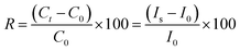
A porous nanostructure surface was fabricated on the half portion of glass substrate using HF-vapor phase etching method with substrate of 50 °C. The details about the vapor phase etching process can be found elsewhere.34 Before depositing the CoPc film, glass substrates were ultrasonically cleaned in the trichloroethylene, acetone and methanol. After that they were dried using the stream of dry argon jet. CoPc films (20 and 60 nm) were deposited using vacuum evaporation on plain and etched glass substrates under a base vacuum of ∼2.0 × 10⁻⁶ Torr. The substrate temperature and deposition rate were kept ∼200 °C and 2 Å s−1, respectively. To study the J–V and gas sensing characteristics of CoPc films, an electrical contact was made using two planer gold electrodes of size 2 mm × 2 mm separated by 12 μm. The thickness of the gold electrodes was kept ∼100 nm. The schematic details of the substrate treatment, CoPc film deposition and Au-electrode fabrication for J–V as well as gas sensing measurements are depicted in Fig. 1. The change in conductance of CoPc film with time (response curves) was recorded in the presence of test gas using a static gas testing setup. CoPc thin film sensors were fixed on the heater mounted in a closed stainless steel chamber of net volume 983 cm3. In order to achieve the desired ppm level of the target gas inside the chamber, a measured quantity of gas was injected using a micro-syringe and recovery of CoPc sensors was obtained by exposing them to ambient air. The conductance with time and J–V characteristics of CoPc films were measured by Keithley 6487 voltage source/picoammeter system using Labview software. The response (R) of the sensor has been calculated by the relative change in the conductance (or electric current) of the sensor using the following equation:2,11| |
 | (1) |
where, Ct and It denote conductance and generated electric current at any time, while, C0 and I0 are base conductance and base current of the CoPc films, respectively.
 |
| | Fig. 1 Schematic representing the steps of porous nanostructured surface formation, CoPc film and Au electrode deposition and electrical circuit for J–V and sensing experiments. | |
The surface roughness and morphology of CoPc films deposited on plain and etched substrate were examined using atomic force microscopy (AFM, Bruker, Nano) and field emission scanning electron microscopy (FESEM, Carl Zeiss, SUPRA 40VP), respectively. The X-ray photoelectron spectroscopy (XPS, DESA-150 Electron Analyzer, Staib Instruments, Germany) of the CoPc films was carried out using Mg Kα with base vacuum of 2 × 10⁻⁹ Torr and the XPS binding energy scale was calibrated using C-1s line at 284.8 eV. The work function of CoPc films was measured by Kelvin Probe technique (SKP 5050, KP Technology Ltd. UK) with gold tip having diameter 2 mm (2 meV resolution). Before measurements, the gold tip work function was calibrated using a standard gold/aluminum sample provided by KP technology. The thickness of CoPc film was measured by 3D profilometer (NanoMap 500 LS AEP Tech.).
3. Results and discussion
3.1. Morphological studies
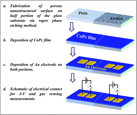
Fig. 2(a) and (b) show the surface morphology of glass substrates before and after etching, respectively. The FESEM image of plain glass exhibits that the surface is very smooth and feature less with σrms = 3 nm, whereas the etched surface consists of randomly distributed nanopores of different sizes as shown in Fig. 2(b). In addition, the value of σrms is increased to ∼7 nm, which is attributed to the formation of porous nanostructured surface on the etched glass. It is believed that CoPc films grown on porous nanostructured surface provide the large surface area for gas adsorption as compared to the CoPc films grown on plain glass. In order to examine the effect of nanoporous surface on film morphology, CoPc films of thickness 20 and 60 nm were grown on plain and etched surface under similar conditions. The FESEM images of these films are presented in Fig. 2(c)–(f). CoPc film of 20 nm grown on plain glass shows granular morphology, and σrms was found to be ∼7 nm. At 60 nm, CoPc grains get elongated, and few places the growth of nanostructured islands can also be seen. In addition, the σrms increased to ∼14 nm (Fig. 2(e)). On the other CoPc films grown on etched surface shows entirely different morphology. FESEM image of CoPc film of 20 nm shown in Fig. 2(d), reveals that films consists of CoPc nanostructured growing in vertical direction, and the σrms was found to be ∼13 nm. With increasing the thickness to 60 nm, these nanostructures grow in size and occupy the all space with σrms = 21 nm as depicted in Fig. 2(f). The role of etched surface during the CoPc film growth is not clear so far and it is under investigated. However, it is believed that nanopores on the etched surface acts as nucleation centers and helps to promote the CoPc nanostructured growth with faster rate. For 60 nm thickness, CoPc films grown on etched surface show fully grown nanostructured surface as compared to CoPc film deposited on plain surface, which is expected to have relatively large numbers of adsorption sites. Therefore, electrical and gas sensing properties of these two CoPc films of thickness 60 nm were further studied. The thickness of CoPc film deposited on glass was further confirmed by 3D profilometer (shown in Fig. 3(a)). The distinguishable step formed between the glass substrate and CoPc film allows the determination of the film thickness. The estimated thickness of CoPc film was found to be ∼63 nm. Moreover, in order to investigate the purity and elemental uniformity, CoPc film has been characterized by various spectroscopy techniques. Further details can be found in the ESI S1 and S2.† In the latter part of this paper, CoPc films grown on plain and etched surface will be termed as CoPc-plain and CoPc-etched film, respectively.
 |
| | Fig. 2 (a) FESEM images of (a) plain glass (b) etched glass (c) 20 nm CoPc film grown on plain glass (d) 20 nm CoPc film grown on etched glass (e) 60 nm CoPc film grown on plain glass (f) 60 nm CoPc film grown on etched glass. | |
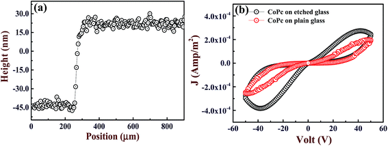 |
| | Fig. 3 (a) Thickness profile of CoPc film deposited on glass substrate. (b) J–V characteristics of CoPc-plain and CoPc-etched films. | |
3.2. Electrical and gas sensing properties
Now we discuss the electrical properties of CoPc-plain and CoPc-etched films. Intrinsically, CoPc film behaves as an insulator but when it exposed to the atmosphere it becomes semiconductor, which is attributed to the chemisorption of ambient oxygen.9,11 The chemisorbed oxygen induces the hole carriers in the CoPc film and enhances its conductivity via following process:| | |
CoPc + O2 ↔ (CoPc + h+) + O2−
| (i) |
CoPc-etched surface is expected to have higher O2− content as compared to CoPc-plain. It is very well reported that the presence of O2− leads to the hysteresis in J–V characteristics by inducing the deep traps in CoPc films.11 Fig. 3(b) shows the J–V characteristics of CoPc-plain and CoPc-etched. As expected, the hysteresis is present in the J–V characteristics for both films, which is attributed to the existence of deep traps induced by O2−. In addition, the hysteresis is more pronounced in case of CoPc-etched film indicating the higher content of adsorbed oxygen due to presence of larger number of CoPc-gas interaction sites as compared to CoPc-plain film (as seen from FESEM images).
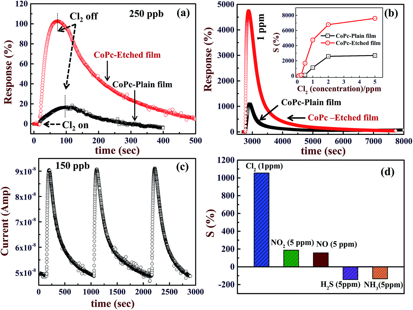
Gas sensing properties of CoPc films are attributed to the fact that exposure of these films to oxidizing gas (e.g. Cl2, NO2 etc.) replaces the O2− (eqn (i)), and promotes more holes in the CoPc film, thereby, its conductivity increases.7,9,11 CoPc films show a reverse behavior if they are exposed to reducing gas (H2S, NH3 etc.). Both CoPc-plain and CoPc-etched films were exposed to different concentrations of Cl2 from 100 ppb to 5 ppm and the corresponding response curves are shown Fig. 4(a) and (b), respectively. The operating temperature was kept at 170 °C to maximize the sensitivity, which will be discussed later. It can be seen that CoPc-plain film can detect Cl2 at 250 ppb level, whereas using CoPc-etched film the detection down to 100 ppb can be achieved. Furthermore, in order to compare the gas sensing properties of CoPc-plain and CoPc-etched films, typical response curves (R as a function of time) has been plotted for 250 ppb and 1 ppm exposure to Cl2 gas, are presented in Fig. 5(a) and (b). These results clearly show that that CoPc-etched film shows better response compared to CoPc-plain film. Sensitivity (S) can be calculated by replacing Ct with Cs in eqn (1), where Cs is the conductance of CoPc film at saturation level. For 250 ppb, the values of S were found to be ∼20 and 105% for CoPc-plain and CoPc-etched films, respectively. For 1 ppm, CoPc-plain film shows S = 1100% and response time ∼90 s, while CoPc-etched film exhibits 4800% and response time ∼54 s. The recovery time was found to be ∼1125 and ∼1170 s for CoPc-plain and CoPc-etched films, respectively. S as function of Cl2 concentration is shown in inset of the Fig. 5(b). It is clear that sensitivity remains significantly higher for CoPc-etched film as compared to CoPc-plain film. These results indicate that gas sensing properties can be improved significantly by producing a suitable nanostructured surface on the substrate. S depends on the available number of gas interaction sites and charge carrier mobility. As seen from FESEM image, CoPc-etched film provides the more interaction sites as compared to CoPc-plain film. However, the mobility of the CoPc-plain film may be higher as compared to the CoPc-etched film, but comparatively large numbers of available sites present enhances the sensitivity of CoPc-etched film. It is to be noted that the nanostructured features size, e.g., pores depth and size may play a very crucial role to manipulate morphology of sensing material film. Therefore, choosing the appropriate thickness of CoPc and nanostructured features such as pores size, depth etc., gas sensing properties can also be improved further.
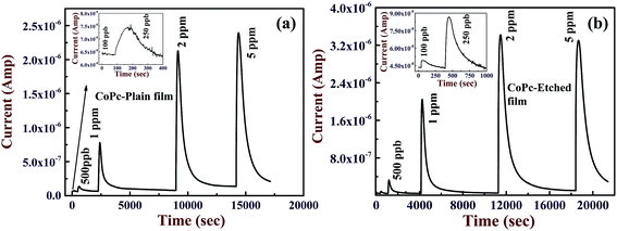 |
| | Fig. 4 Response curves for different Cl2 doses of (a) CoPc-plain film (b) CoPc-etched film. Insets represent the magnified response curve in 100–250 ppb range. | |
 |
| | Fig. 5 Response curves (at 170 °C) for CoPc-etched and CoPc-plain films for (a) 250 ppb (b) 1 ppm (inset shows S as a function of Cl2 concentration for CoPc-plain and CoPc-etched films) (c) response curves for CoPc-etched film for repeated exposures to 150 ppb Cl2. (d) Bar chart displaying the sensitivity for different oxidizing and reducing gases, which reveals high selectivity of CoPc-etched film to Cl2 gas. | |
The other gas sensing properties such as reproducibility, selectivity, temperature dependent sensitivity of CoPc-etched film surface were also investigated. To test the reproducibility of the response, CoPc-etched film was exposed to a known concentration of Cl2 dose (150 ppb), the results obtained are shown in Fig. 5(c). It can be seen that the response remains nearly same on repeated exposure of Cl2 gas, which shows that the response curves are reproducible. The sensitivity of CoPc-etched film was tested for various oxidizing and reducing gases, the results are shown in the Fig. 5(d). These results show that CoPc-etched film is highly selective to Cl2 gas. The good sensitivity of the CoPc film towards Cl2 is attributed to high value of electronegativity (electron acceptor nature) and strong oxidizing nature of chlorine as compared to other gases. Cl2 can replace the adsorbed oxygen very easily and get adsorbed at other free sites on the CoPc films surface. Therefore, CoPc film sensor has well selectivity towards chlorine Cl2 against other gases. The gas sensing properties strongly depend on the working temperature of the sensor. To optimize the working temperature, we have measured the response curves at different operating temperatures for a concentration of 250 ppb and the corresponding results are presented in Fig. 6. It can be seen that S (shown in the inset of Fig. 6) increases with increasing the operating temperature till ∼170 °C. With further increasing the operating temperature the sensitivity decreases. Above room temperature (>100 °C), the enhancement in S value may be attributed to the desorption of chemisorbed oxygen from CoPc film surface. This desorption process, thus, provides additional fresh active interaction sites for Cl2 and also reduced the number of deep traps induced by oxygen. The decrease in the S value sensitivity above 170 °C may be ascribed to the fact Cl2 desorbs with higher rate as compared to its adsorption at CoPc film surface. These results are in good agreement with the reported results for MPcs films.6,10,35 The recovery time continuously decreases with increasing the temperature. At low temperature (up to 135 °C), CoPc films could not recover its base conductance even after 2000 seconds. These results shows that at 170 °C, the CoPc films shows maximum sensitivity with full recovery, therefore, the gas sensing properties were studied at this optimum operating temperature.
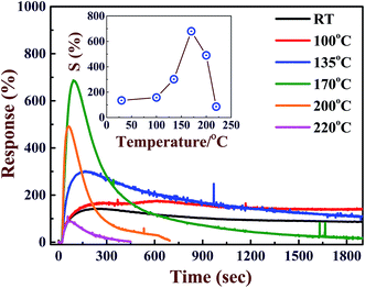 |
| | Fig. 6 Response curve of CoPc-etched film for 500 ppb Cl2 exposure at different temperatures. Inset shows the value of S as function of operating temperature. | |
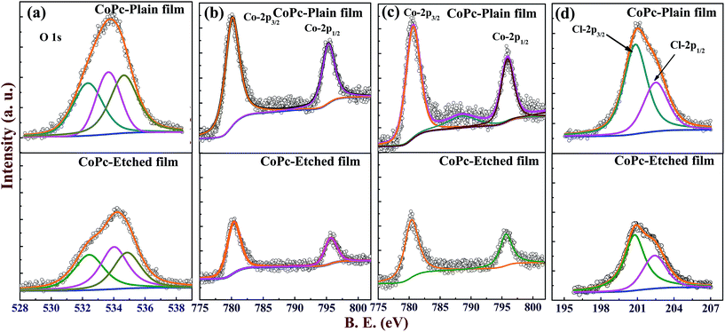
3.3. XPS and Kelvin probe measurements
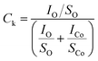
To get more insight about the interaction sites the XPS data of CoPc-plain and CoPc-etched films were recorded. The core level O 1s and Co-2p XPS spectra for both films (before Cl2 exposure) are presented in Fig. 7(a) and (b). The core level O 1s peak CoPc is deconvoluted into three different peaks at 532.3, 533.6 and 534.6 eV, which are attributed to physisorbed oxygen, chemisorbed oxygen O2− and adsorbed moisture, respectively.11 The Co-2p can be resolved into two peaks 2p3/2 and 2p1/2 at 780.3, and 795.4 eV, respectively. To compare the content of adsorbed oxygen at the CoPc-plain and CoPc-etched films surface, the physisorbed and chemisorbed oxygen composition (Ck) relative to Co (central metal atom) was quantified using the relation:2,36| |
 | (2) |
where I and S are intensity and atomic sensitivity factors, respectively, and the subscript denotes the corresponding elements. To determine the intensities of the adsorbed oxygen (physisorbed and chemisorbed) and Co peaks, the total area under the core level peaks was calculated using the least-squares fitting of Gaussian line shape.2 The values of sensitivity factor were taken 0.63 and 4.50 for O 1s and Co 2p peaks, respectively.36,37 The quantification of XPS results showed the total concentration of absorbed oxygen was found to be 72% (chemisorbed 33%, physisorbed 39%) and 85% (chemisorbed 41% and physisorbed 44%) for CoPc-plain and CoPc-etched film, respectively. Moreover, it is very well reported that central metal atom of MPcs plays an important role in gas sensing characteristics and it is the main attacking site for the Cl2.7,9 Therefore, in order to compare the available number of Cl2 interaction sites, both the films were exposed to 20 ppm of Cl2 concentration for a duration of 5 min at 170 °C, and after that they were cooled down to room temperature. Fig. 7(c) and (d) show XPS spectra of Co 2p and Cl 2p for CoPc-plain and CoPc-etched film after the Cl2 exposure. Cl 2p peak after the exposure was found to be in both cases, which is deconvoluted into two peaks present at 200.1 and 202.4 eV, corresponding to Cl 2p3/2 and Cl 2p1/2. As the central atom in MPcs is the main reaction site for Cl2 gas molecule, therefore, the peak intensity ratio of Cl 2p and Co 2p should be higher for the more sensitive film. The XPS quantification of Cl2 was calculated using the eqn (2) and it was found to be ∼88 and ∼93% for CoPc-plain and CoPc-etched, respectively. These results show that CoPc-etched film provides more interaction sites for the gas adsorption as compared to CoPc-plain, which improves its gas sensing characteristics.
 |
| | Fig. 7 XPS spectra recorded for fresh CoPc-plain and CoPc-etched film (a) O 1s and (b) Co 2p. XPS spectra recorded for CoPc-plain and CoPc-etched film after Cl2 exposure (c) Co 2p and (d) Cl 2p. | |
Furthermore, Cl2 exposure on CoPc films affects the charge carrier concentration, and it should be reflect in work function (ϕ) measurements. To determine ϕ of the sample (CoPc film), the contact potential difference (VCPD) between tip and sample was measured. VCPD is developed via equilibrium, if an electrical contact is made between tip and the sample, which can be defined as:
| |
 | (3) |
where,
ϕtip and
ϕsample represent the respective work function of the tip and sample.
38 The tip was allowed to vibrate with a frequency (
ω = 78.3 Hz) just above the sample surface, which produces a periodic change in capacitance (d
C/d
t). Therefore, on the application of an external voltage (
Vext) to the tip, electric current flows in the circuit, which can be expressed by following equation:
| |
 | (4) |
At a unique point Vext = VCPD, the null condition (i(t) = 0) is obtained, and hence, the VCPD can be estimated. Since, ϕtip is known (from calibration), ϕsample can be calculated using eqn (3). In order to compare the effect Cl2 gas, work function of both CoPc-plain and CoPc-etched films were measured before and after the Cl2 exposure. Tip was scanned in raster fashion across the CoPc film surface of area 2 mm2 and the relative variation in VCPD was measured to obtain the better average result. Both films were exposed to same concentration (20 ppm) and kept in a close chamber for ∼5 min. The 3D (three dimensional) images of work function for both CoPc films before and after Cl2 exposure is presented in Fig. 8(a). Before exposure, CoPc films grown on both substrates shows nearly identical value of ϕ and after the exposure it increases in both cases. This increase in the work function (ΔϕCoPc) is ascribed to the p-type nature of CoPc molecule and an increase in holes concentration on the exposure of Cl2 gas forces the Fermi level to move towards EHOMO (highest occupied molecular orbital). An energy level diagram showing the effect of Cl2 gas exposure is presented in Fig. 8(b). After Cl2 exposure CoPc-plain and CoPc-etched show ΔϕCoPc ∼ 270 meV and 345 meV, respectively (Fig. 8(a)). Relatively higher value of ΔϕCoPc for CoPc-etched film confirms that more carriers are produced after the exposure for the same amount of Cl2 gas. Kelvin probe results further support that CoPc-etched surface has large number of gas-material interaction sites, which improves its gas sensing properties. We believe that controlling the features of porous nanostructured surface, e.g., pore size, depth etc., and using an appropriate substrate the sensitivity can be improved further and detection limit as low as 5 ppb can be achieved. Therefore, this study paves a new avenue for the application of surface etching process to improve the gas sensing properties of organic semiconductor thin film based sensors.
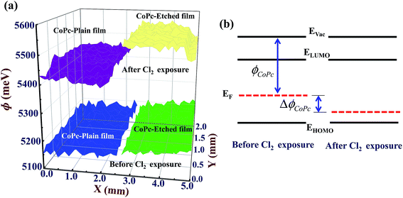 |
| | Fig. 8 (a) Work function images of CoPc-plain and CoPc-etched films before and after the Cl2 exposure. (b) The energy level diagram showing the shift in Fermi level (work function, ΔϕCoPc) due to the Cl2 exposure. | |
4. Conclusions
In conclusion, we have demonstrated the utilization of surface etching process to improve the gas sensing properties of organic semiconductor thin film based sensor. A porous nanostructured surface was fabricated via vapor phase etching method. FESEM results showed that CoPc nanostructures grow with faster rate on etched surface, which is attributed to the presence of nanopores on the surface and the surface of CoPc-etched film was found to be less smooth with respect to CoPc-plain film. For 60 nm, CoPc-etched film showed ∼5 times enhanced sensitivity as compared to CoPc-plain for the exposure of 250 ppb of Cl2. The CoPc-etched film was able to detect the Cl2 gas down to 100 ppb, which is superior to CoPc-plain film. The improved gas sensing characteristics of CoPc-etched film is attributed to the presence of large number of active gas-material sites as compared to CoPc-plain film. The presence of relatively large number of gas-material interaction sites at CoPc-etched film was confirmed by charge transport, XPS and work function measurement. It is believed that fabricating the suitable nanostructure on appropriate substrate the gas sensing properties such as sensitivity, low detection limit etc., can be improved further.
Acknowledgements
The authors are thankful to the Director, CSIR-NAL for his support and encouragement.
References
- D. R. Klonne, C. E. Ulrich, M. G. Riley, T. E. Hamm Jr, K. T. Morgan and C. S. Barrow, Fundam. Appl. Toxicol., 1987, 9, 557–572 CrossRef CAS PubMed.
- R. Saini, A. Mahajan, R. K. Bedi, D. K. Aswal and A. K. Debnath, Sens. Actuators, B, 2014, 198, 164–172 CrossRef CAS.
- R. B. R. Mesquita, M. L. F. O. B. Noronha, A. I. L. Pereira, A. C. F. Santos, A. F. Torres, V. Cerda and A. O. S. S. Rangel, Talanta, 2007, 72, 1186–1191 CrossRef CAS PubMed.
- V. D. Sickle, M. A. Wenck, A. Belflower, D. Drociuk, J. Ferdinands, F. Holguin, E. Svendsen, L. Bretous, S. Jankelevich, J. J. Gibson, P. Garbe and R. L. Moolenaar, Am. J. Emerg. Med., 2009, 27, 1–7 CrossRef PubMed.
- D. D. Eley, Nature, 1948, 162, 819 CrossRef CAS PubMed.
- T. Miyata, S. Kawaguchi, M. Ishii and T. Minami, Thin Solid Films, 2003, 425, 255–259 CrossRef CAS.
- J. D. Wright, Prog. Surf. Sci., 1989, 31, 1–60 CrossRef CAS.
- Y. Acikbas, M. Evyapan, T. Ceyhan, R. Capan and O. Bekaroglu, Sens. Actuators, B, 2007, 123, 1017–1024 CrossRef CAS.
- F. I. Bohrer, C. N. Colesniuc, I. K. Schuller, J. Park, A. C. Kummel, M. E. Ruidiaz and W. C. Trogler, J. Am. Chem. Soc., 2009, 131, 478–485 CrossRef CAS PubMed.
- D. K. Aswal and J. V. Yakhmi, Molecular and Organic Electronics Devices, Nova Science Publishers, New York, NY, USA, 2010 Search PubMed.
- S. Samanta, A. Kumar, A. Singh, A. K. Debnath, D. K. Aswal and S. K. Gupta, Chem. Pap., 2012, 66, 484–491 CAS.
- E. Kaki, A. Altindal, B. Salih and O. Bekaroglu, Dalton Trans., 2015, 44, 8293–8299 RSC.
- R. Saini, A. Mahajan, R. K. Bedi, D. K. Aswal and A. K. Debnath, RSC Adv., 2014, 4, 15945–15951 RSC.
- F. I. Bohrer, C. N. Colesniuc, J. Park, I. K. Schuller, A. C. Kummel and W. C. Trogler, J. Am. Chem. Soc., 2008, 130, 3712–3713 CrossRef CAS PubMed.
- T. Miyata and T. Minami, Appl. Surf. Sci., 2005, 244, 563–567 CrossRef CAS.
- L. Tingping, S. Yunbo, L. Wenlong, L. Yang, Y. Pengliang, L. Liwei, S. Daoheng, T. Wei and W. Liquan, J. Semicond., 2010, 31, 080010–080015 Search PubMed.
- A. Kumar, A. K. Debnath, S. Samanta, A. Singh, R. Prasad, P. Veerender, S. Singh, S. Basu, D. K. Aswal and S. K. Gupta, Sens. Actuators, B, 2012, 171, 423–430 CrossRef.
- A. Kumar, N. Joshi, S. Samanta, A. Singh, A. K. Debnath, A. K. Chauhan and D. K. Aswal, Sens. Actuators, B, 2015, 206, 653–662 CrossRef CAS.
- A. Altindal, Z. Z. Ozturk, S. Dabak and O. Bekaroglu, Sens. Actuators, B, 2001, 77, 389–394 CrossRef CAS.
- T. Patois, J.-B. Sanchez, F. Berger, P. Fievet, V. Moutarlier, M. Bouvet, B. Lakard and O. Segut, Talanta, 2013, 117, 45–54 CrossRef CAS PubMed.
- X. Liang, Z. Chem, H. Wu, L. Guo, C. He, B. Wang and Y. Wu, Carbon, 2014, 80, 268–278 CrossRef CAS.
- P. Jha, M. Sharma, A. Chouksey, P. Chaturvedi, D. Kumar, G. Upadhyaya, J. S. B. S Rawat and P. K. Chaudury, Synth. React. Inorg. Met.–Org. Chem., 2014, 44, 1551–1557 CrossRef CAS.
- Y. Wang, N. Hu, Z. Zhou, D. Xu, Z. Wang, Z. Yang, H. Wei, E. S.-W. Kong and Y. Zhang, J. Mater. Chem., 2011, 21, 3779–3787 RSC.
- J. Tamaki, J. Niimi, S. Ogura and S. Konishi, Sens. Actuators, B, 2006, 117, 353–358 CrossRef CAS.
- A. Chaparadza and S. B. Rananavare, Nanotechnology, 2008, 19, 245501–245508 CrossRef PubMed.
- J. Tamaki, C. Naruo, Y. Yamamoto and M. Matsuoka, Sens. Actuators, B, 2002, 83, 190–194 CrossRef CAS.
- D. R. Patil and L. A. Patil, Sens. Actuators, B, 2007, 123, 546–553 CrossRef CAS.
- D. H. Dawson and D. E. Williams, J. Mater. Chem., 1996, 6, 409–414 RSC.
- C. V. Gopal Reddy, S. V. Manorama and V. J. Rao, Sens. Actuators, B, 1999, 55, 90–95 CrossRef CAS.
- K. Garg, A. Singh, A. K. Debnath, S. K. Nayak, S. Chattopadhyay, D. K. Aswal, Y. Hayakawa, S. K. Gupta and J. V. Yakhmi, Chem. Phys. Lett., 2010, 488, 27–31 CrossRef CAS.
- P. Rao, R. V. Godbole and S. Bhagwat, J. Magn. Magn. Mater., 2016, 405, 219–224 CrossRef CAS.
- A. Joshi, D. K. Aswal, S. K. Gupta, J. V. Yakhmi and S. A. Gangal, Appl. Phys. Lett., 2009, 94, 103115 CrossRef.
- A. K. Sharma, R. Saini, R. Singh, A. Mahajan, R. K. Bedi and D. K. Aswal, AIP Conf. Proc., 2014, 1591, 671–673 CrossRef CAS.
- A. Kumar, S. Siddhanta and H. C. Barshilia, Sol. Energy, 2016, 129, 147–155 CrossRef CAS.
- G. Guillaud, J. Simon and J. P. Germain, Coord. Chem. Rev., 1998, 467, 178–180 Search PubMed.
- J. F. Moulder, W. F. Stickle, P. E. Sobol and K. D. Bomben, Handbook of X-ray Photoelectron Spectroscopy: A Reference Book of Standard Spectra for Identification and Interpretation of XPS Data, Physical Electronics Publisher, 1995 Search PubMed.
- C. D. Wagner, L. E. Davis, M. V. Zeller, J. A. Taylor, R. H. Raymond and L. H. Gale, Surf. Interface Anal., 1981, 3, 211–225 CrossRef CAS.
- Y. Rosenwaks, R. Shikler, T. Glatzel and S. Sadewasser, Phys. Rev. B: Condens. Matter Mater. Phys., 2004, 70, 085320–085326 CrossRef.
Footnote |
| † Electronic supplementary information (ESI) available. See DOI: 10.1039/c6ra25185d |
|
| This journal is © The Royal Society of Chemistry 2017 |
Click here to see how this site uses Cookies. View our privacy policy here. 
 Open Access Article
 This Open Access Article is licensed under a
  a,
Soumen Samantab,
S. Lathaa,
A. K. Debnathb,
Ajay Singhb,
K. P. Mutheb and
Harish C. Barshilia*a
a,
Soumen Samantab,
S. Lathaa,
A. K. Debnathb,
Ajay Singhb,
K. P. Mutheb and
Harish C. Barshilia*a