
 Open Access Article
 This Open Access Article is licensed under a Creative Commons Attribution-Non Commercial 3.0 Unported Licence
Effect of UV-ozone process on the ZnO interlayer in the inverted organic solar cells†
Dou Liab,
Wenjing Qin *ab,
Shengchen Zhangab,
Dongyue Liuab,
Zhenyang Yuc,
Jing Maod,
Linfeng Wuab,
Liying Yang*ab and
Shougen Yin*ab
*ab,
Shengchen Zhangab,
Dongyue Liuab,
Zhenyang Yuc,
Jing Maod,
Linfeng Wuab,
Liying Yang*ab and
Shougen Yin*ab
aKey Laboratory of Display Materials and Photoelectric Devices, Education Ministry of China, School of Materials Science and Engineering, Tianjin University of Technology, Tianjin 300384, China. E-mail: wjqin@tjut.edu.cn; liyingyang@tjut.edu.cn; sgyin@tjut.edu.cn
bTianjin Key Laboratory for Photoelectric Materials and Devices, Tianjin University of Technology, Tianjin 300384, China
cSchool of Mechanical Engineering, Tianjin Polytechnic University, Tianjin, 300384, China
dInstitute of New-Energy Materials, Key Laboratory of Advanced Ceramics and Machining Technology, Ministry of Education, School of Materials Science and Engineering, Tianjin University, Tianjin, 300072, China
First published on 18th January 2017
Abstract
ZnO interlayer is crucial for the performance of inverted organic solar cells (IOSCs). Herein, we investigate the effects of short UV-ozone treatment of ZnO nanofilms (ZnONFs) on the performance of IOSCs with a structure of ITO/ZnONFs/P3HT:PCBM/MoO3/Ag. There is a 17.59% and 32.60% increase in the short circuit current and power conversion efficiency, respectively, after the treatment of the device for 20 seconds. Furthermore, the optimized device showed excellent stability under ambient conditions for more than four weeks without encapsulation. We conclude that the UV-ozone treatment oxidizes oxygen vacancy defects of ZnONFs, thereby decreasing the internal resistance and improving charge transfer at the ZnONFs/polymer interface. However, a longer treatment time will produce oxygen interstitial defects, which dramatically increases the work functions of ZnONFs and deteriorates the contact between ZnONFs and the active layer. As a result, the process of charge transfer will be blocked, resulting in a sharp drop in the performances of IOSCs.
Introduction
Semiconductor materials have drawn special attention, both as a result of fundamental interest and potential applications, especially in the field of solar energy conversion.1–4 Among these materials, ZnO is a good candidate for photovoltaic devices because of it is low-cost, environmentally-friendly, and possesses high optical transmittance in the visible range,5 and high electronic mobility (100 cm2 (V−1 s−1) at least).6 For example, ZnO nanofilms (NFs) have been used as electron-selective layers in the inverted organic solar cells (IOSCs).However, many challenges still remain. Note that ZnONFs have a large number of surface defects such as oxygen vacancies (VO) and oxygen interstitial species (Oi).7,8 Previous studies have stated that the grain boundary properties and optoelectronic properties of ZnONFs are significantly influenced by the density and condition of these defects, especially VO for its largest number.9 Thus, it can be concluded that in the case ZnONFs incorporated into the solar cells, these defects will influence the behavior of the carriers, which will alter the J–V characteristics of the devices. For example, VO are known to be the donor defects, which can capture the photo-induced carriers;7,8 therefore, these defects give rise to a high density of recombination centers, resulting in the decrease of short current density (JSC).10,11 Moreover, VO defects influence the work functions (WFs) of ZnONFs by decreasing the crystallinity, leading to a mismatch in the energy levels of the devices.12,13 However, Oi defects are a type of acceptor defects with level position close to the valence band of ZnO.14 These defects have a tendency to capture holes in the active layers and the photoinduced electrons travel through the ZnONFs. They will push the ZnO Fermi-level further away from the vacuum level, causing a smaller built-in potential.15 These result in a deteriorated performance of the devices. The adverse impact of the Oi defects is a less smooth carrier transmission. In addition, these surface defects can promote photocatalysis, which can degrade the photoactive layer at the surface of the ZnONFs and eventually reduce the lifetime of the IOSCs.
In the past, researchers have attempted many methods aimed at deflecting passivation, such as UV-ozone treatment,10,11,13 atomic doping,9,16–18,23 surface modification,19,20 and annealing treatments,21 etc. The electrical conductivity of the ZnONFs has been significantly improved by suppressing the VO defects.19,22 Thus, passivation of VO defects is in favor of enhancing the performances of the devices. Compared with these methods, UV-ozone treatment is regarded as an effective way to alter the surface states and modify the defects of ZnONFs without any additives. However, Sai Bai and co-workers proved that long-time (15 min) UV-ozone treatment on the ZnONFs caused an increase in the WFs (0.6 eV), whereas the power conversion efficiency (PCE) of the device decreased from 4.17 to 2.35%.13 To the best of our knowledge, the mechanism behind the effects of UV-ozone treatment on the improvement of charge transport and device performance is not fully understood.
In this study, we performed a short UV-ozone treatment on the ZnONFs to study the effects on the surface states, defects, and WFs. Our results indicated that the VO defects in ZnONFs reduced by filling with reactive oxygen species produced by UV-ozone treatment. However, when the UV-ozone treatment continued to 30 s, the VO surface defects became saturated, such that active oxygen began to enter the lattice, generating Oi. These defects have a significant impact on the surface WFs and electronic conductivity of the ZnONFs. Consequently, the PCE of the inverted solar cell, which incorporated ZnONFs after a 20 s UV-ozone treatment as an electron transport layer, increased about 32.60% in comparison to that of the untreated solar cells. At the same time, the environmental stability of the devices was remarkably improved.
Experimental
ZnONFs were synthesized through a facile sol–gel process as reported by many researchers.19–22 The IOSC devices with a structure of indium tin oxide (ITO)/ZnONFs/poly(3-hexylthiophene):(6,6)-phenyl-C61-butyric acid methyl ester (P3HT:PCBM)/molybdenum oxide (MoO3)/Ag were then fabricated. ITO-coated glass substrates were cleaned in an ultrasonic bath with acetone and isopropyl alcohol for 20 min each, rinsed with deionized water, and then blew-dried with nitrogen. The ZnO precursor solution was spin-coated on the top of the ITO-coated glass with a speed of 2000 rpm for 30 s. The coating procedure was repeated 2 times to obtain a thicker layer. After getting deposited by spin coating, the films were annealed at 150 °C for 1 h in a vacuum oven. Then, ZnONFs were rinsed with deionized water by ultrasonication to remove the residual inorganic salt from the surface. After the ZnONFs were completely dried, these were submitted to UV-ozone treatment for different time intervals (0, 10, 20, and 30 s) and were then referred to as ZnO, ZnO-10, ZnO-20, and ZnO-30, respectively. The blend of P3HT and PCBM (1![[thin space (1/6-em)]](https://www.rsc.org/images/entities/char_2009.gif) :0.8 weight-ratio) in a 1,2-dichlorobenzene solution was spin-coated on the ZnONFs at 800 rpm for 12 s in a glove box to form the active layer. The samples were then thermally annealed at 110 °C for 10 min under vacuum. Finally, 2 nm molybdenum oxide (MoO3) buffer layer and 100 nm Ag layer were thermally deposited in vacuum (∼4 × 10⁻⁴ Pa). The area of the active layer of the device was 0.09 cm2, as defined by a shadow mask. The device without UV-ozone processing was used as the control.
:0.8 weight-ratio) in a 1,2-dichlorobenzene solution was spin-coated on the ZnONFs at 800 rpm for 12 s in a glove box to form the active layer. The samples were then thermally annealed at 110 °C for 10 min under vacuum. Finally, 2 nm molybdenum oxide (MoO3) buffer layer and 100 nm Ag layer were thermally deposited in vacuum (∼4 × 10⁻⁴ Pa). The area of the active layer of the device was 0.09 cm2, as defined by a shadow mask. The device without UV-ozone processing was used as the control.
PSD Pro series Digital UV ozone system (PSD PRO-UV6T) was used to perform the UV-ozone treatment. The power of the UV lamp at 254 nm was 30 mW cm−2 and the oxygen flow rate was 5 L min−1. The process was controlled for 10 s. The surface morphology and roughness of the ZnONFs were characterized by Bruker Innova atomic force microscope (AFM). The static contact angles of ZnONFs were measured by sessile drop method using a DSA100 Drop Shape Analysis System (KRUSS GmbH, Germany) and all instruments were controlled by the DSA 3 analysis software. The work functions (WFs) of ZnONFs were evaluated by Kelvin Probe method in air using a KP 020 Ambient Kelvin Probe system. X-ray photoelectron spectroscopy (XPS) studies were conducted using a Thermo Fisher K-Alpha measurement system with a monochromatic Mg Kα X-ray source (hν = 1486.6 eV) and a charge neutralizer. Extended spectra (survey) were obtained in the range of 0–1100 eV (187.85 eV pass energy). The transmission spectra of ZnONFs and ultraviolet-visible (UV-vis) absorption spectra of ZnONFs/P3HT:PCBM were obtained using a Hitachi U-4100 UV-visible spectrophotometer. Photoluminescence (PL) spectroscopy and the time-resolved photoluminescence (TRPL) of ITO/ZnONFs/P3HT:PCBM were performed using a Jobin Yvon FL 3-221-TC SPC fluorescence spectrophotometer. The incident photon-to-current efficiency (IPCE) spectra were obtained using a CROWNTHEC IPCE test system. The J–V curves of the unencapsulated devices were obtained under short circuit conditions in ambient atmosphere with white light illumination intensity of 100 mW cm−2 created using a 300 W solar simulator (Thermal Oriel 91160) with an AM1.5G filter. The light intensity was calibrated with an Oriel mono-Si reference cell (CROWNTECH PVM 272 certificated by NREL). The J–V curves were swept with a Keithley 2400 source meter from −1 to +1 V in steps of 10 mV at a rate of 0.1 s per step until a stable efficiency was achieved. The I–V curves of ZnONFs were swept with a Keithley 2400 source meter from −4.5 to +4.5 V in steps of 20 mV at a rate of 0.1 s per step until stable efficiency was achieved. The thickness of the ZnONFs was measured using a KLA Tencor D-100.
Results and discussion
The illuminated current density–voltage (J–V) characteristics of the IOSCs based on ZnONFs are shown in Fig. 1a, and the detailed photovoltaic parameters are summarized in Table 1. The control device containing the untreated ZnO showed a JSC value of 10.52 mA cm−2, an open-circuit voltage (VOC) of 0.59 V, a fill factor (FF) of 58%, and a PCE of 3.62%. After UV-ozone treatment, the performance of the device gradually improved. The device based on ZnO-20 showed the best performance, with a JSC value of 12.37 mA cm−2, VOC of 0.59 V, FF of 66%, and PCE of 4.80%. The improvement in the PCE mainly originated from the increased JSC and FF. The values of series resistance (Rs) and shunt resistance (Rsh) are also shown in Table 1. The value of Rs decreased from 1.70 for ZnO to 1.53 Ω cm2 for ZnO-20, whereas the Rsh increased from 65.44 to 70.02 Ω cm2. The decrease of Rs and increase of Rsh indicated that the UV-ozone treatment helped in improving the charge selectivity and suppressed charge combination at the interface, resulting in enhanced JSC and FF. However, on continued treatment with UV-ozone, JSC value of the device decreased. This demonstrates that the electronic conduction ability is deteriorated with longer UV-ozone treatment time, which leads to a poor carrier transmission. This result illustrated the dependence of the performance of the IOSC on the treatment time.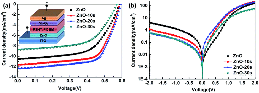 | ||
| Fig. 1 (a) and (b) J–V characteristics of the IOSCs with ZnONFs UV-ozone treated for different times under 100 mW cm−2 illumination and in the dark, respectively. | ||
| Device | VOC (V) | JSC (mA cm−2) | FF (%) | PCE (%) | Rsh (Ω cm2) | Rs (Ω cm2) |
|---|---|---|---|---|---|---|
| ZnO | 0.59 | 10.52 | 58 | 3.62 | 65.44 | 1.70 |
| ZnO-10 | 0.59 | 11.64 | 65 | 4.49 | 66.66 | 1.55 |
| ZnO-20 | 0.59 | 12.37 | 66 | 4.80 | 70.02 | 1.53 |
| ZnO-30 | 0.57 | 8.91 | 57 | 2.90 | 61.77 | 1.69 |
Fig. 1b shows the dark J–V curve of the IOSC. With extended treatment time, the backward current was gradually reduced, which means that the reverse flow of electrons was suppressed after the UV-ozone treatment. The forward current first increased with 10 s and 20 s of UV-ozone treatment. The devices treated with UV-ozone for 20 s demonstrated a more ideal diode behavior and lower reverse bias leakage with respect to the device based on ZnO, indicating less ohmic loss and better charge selectivity for the whole device. The decreasing tendency of the dark current under forward bias after 30 s UV-ozone treatment indicated that charge forward transfer may be blocked for some reason. This result is consistent with the illuminated J–V characteristics.
The enhanced performance in the UV-ozone treated devices could originate from two sources: a decrease in the interfacial defects (traps or recombination centers) or change in the band alignment between ZnONFs and active layer.24 Formation of the active layer is known to be rather sensitive to the underlying interfacial layer. Thus, the morphology of the ZnONFs was investigated by AFM and profile-system (Fig. S1a–d in the ESI†). The thickness of the ZnONFs were 187.3 nm, 185.5 nm, 188.8 nm, and 186.5 nm. The surface roughness was 3.19 ± 0.01 nm, 4.39 ± 0.01 nm, 3.59 ± 0.02 nm, 3.06 ± 0.01 nm, and the average size was about 15.74 nm, 16.45 nm, 16.89 nm, and 16.92 nm, corresponding to ZnO, ZnO-10, ZnO-20, and ZnO-30, respectively. Therefore, we concluded that the film thickness, surface roughness, and particle size were not greatly affected by the UV-ozone treatment. Water contact angle measurements were also used to study the surface properties of ZnONFs. The contact angles between water and ZnONFs were slightly decreased from 71.75 to 63.08° and the surface energies increased from 40.7 mN m−1 to 45.7 mN m−1 after the UV-ozone treatment (Fig. S1e–h†). UV-ozone treatment usually improved the hydrophilic property of the ZnO materials, which can decompose the residual organics at the surfaces of the materials. Therefore, the surface hydrophilicity slightly increased after the treatment, which would lead to an undesirable interfacial contact between the P3HT:PCBM layer and the upper active layer, albeit with degenerated morphology and less contact. The bad interface may lead to the generation of interface defects, which then block the transportation of electrons and, finally, cause a decoration of the device.
The WFs of the ZnO control and the UV-ozone treated ZnO were measured using a Kelvin probe. The result is shown in Table S1 and Fig. S2,† the surface WFs are 4.71, 4.75, 4.80, and 4.83 eV for ZnO, ZnO-10, ZnO-20, and ZnO-30, respectively. The result demonstrated that UV-ozone treatment of ZnONFs induced a continuous increase in the work functions. To further investigate the effect of UV-ozone on the work function of ZnO, we extend the treatment time to 30 minutes. It can be seen in Fig. S2† that the WFs increased with the increase of treatment time in the first 30 minutes. After this, WFs achieved a value of 5.33 ± 0.1 eV and tended to be saturated. The increase of WFs caused larger built-in potential and made ZnONFs more facile for the extraction of electrons from PCBM. As a result, electron can more effectively transfer from the polymer blend to the ZnONFs and subsequently travel to the electrodes.
Note that we also measured ITO WFs under UV-ozone process. It was obvious that in addition to UV irradiation, ITO WFs produced a slight increase. The difference between the WFs for ZnONFs and ITO and their interfacial band alignment are also shown in the Table S1† and Fig. 2. It can be seen that after the UV-ozone treatment, the type of interface between ZnONFs and ITO changed from Schottky contact to ohmic contact, which means that the electron transmission from ZnONFs to ITO electrode will become more smooth and the blocking effect of the hole will be more significant. The wider the difference of WFs, the larger the band bending of ZnONFs at the interface, and the property of forward conduction and reverse blocking is more obvious. The result was consistent with the dark J–V curve of the backward bias. However, the initial increase and subsequent decrease in the JSC and dark current at forward bias may be caused by a combination of factors, such as deterioration of the interface and interfacial band alignment. Further increase in the UV-ozone treatment time, as reported in ref. 15, induced the formation of p-type defects, pushing the WFs of the ZnO layer further away from the vacuum level and decreasing the wurtzite crystallinity.
 | ||
| Fig. 2 Interfacial band alignment between ZnONFs and ITO electrode before (a) and after 30 s UV-ozone treatment (b). (c) I–V characteristics of the structure of ITO/ZnONFs with and without UV-ozone treatment. | ||
To deeply explain the influence of UV-ozone treatment on the electronic transmission, XPS spectra were obtained to investigate the composition and defects reparation of ZnONFs during the treatment. Fig. 3 shows the O 1s region of ZnO with and without UV-ozone treatment. The peak at the binding energy of 530 eV (low-binding-energy, LB) was attributed to the O 1s level in the Zn–O bond, the 531.8 eV (middle-binding-energy, MB) was associated with oxygen (O2) adsorbed in the oxygen-deficient regions25 or VO defects,26 and the peak at 532.4 eV (high-binding-energy, HB) corresponded to interstitial oxygen (Oi). The ratios of peak area of LB to HB were approximately 1:1:0, 18:12:1, 13:8:1, and 4:0.6:1 for ZnO, ZnO-10, ZnO-20, and ZnO-30, respectively. With the extension of treatment time, the Zn–O bond was successively enhanced, illustrating that the UV-ozone treatment can passivate the VO defects to increase the Zn–O bond. During processing, some free oxygen atoms can be produced under ultraviolet irradiation (formula (1)), which then penetrates into the inner ZnONFs, ultimately taking possession of the VO defects. When the oxygen-deficiency was repaired, the transfer of electrons from ZnONFs to ITO electrode was expected to occur much more smoothly.
| O2 + O2 ⇌ O3 + O | (1) |
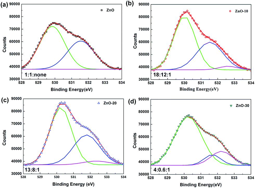 | ||
| Fig. 3 The high-resolution XPS spectra of O 1s for ZnONFs (a) ZnO, (b) ZnO-10, (c) ZnO-20, and (d) ZnO-30. | ||
The peak area of HB increased dramatically upon extending the treatment time. It may be because the oxygen atoms penetrate into ZnONFs and then embed in the lattices to generate the Oi defects when the VO defects are gradually being filled and the oxygen atoms become redundant.27 The re-increased defects density finally leads to the worse performance.
To gain more insight into how UV-ozone treatment passivated and repaired the VO defects and then increased the Oi defects, we investigated the optical properties of ZnONFs. Fig. 4a shows the optical transmittance spectra of ZnONFs with and without the treatment. All of the ZnONFs exhibited good transmittance in the visible range from 300 to 800 nm with the average transmittance values of about 90%. This indicated that the light incidence into the active layer was not influenced by the UV-ozone treatment. The absorption spectra of the structure of ITO/ZnONFs/P3HT:PCBM also supported this conclusion since the curve underwent little change in shape and intensity (Fig. 4a).
 | ||
| Fig. 4 (a) Optical transmission spectra of ZnONFs and optical absorption spectra of P3HT thin films for ITO/ZnONFs/P3HT:PCBM structures, (b) PL spectra of ZnONFs, (c) IPCE of solar cells with ZnONFs, and (d) TRPL spectra of ITO/ZnONFs/P3HT:PCBM structures. | ||
Fig. 4b shows the photoluminescence (PL) spectra of ZnONFs with and without the UV-ozone treatment obtained at an excitation wavelength of 340 nm. The intensity of the PL spectrum of ZnONFs powders with 20 s treatment was significantly weaker than that of the other samples. In the spectral range of 520–570 nm, the PL intensity decreased by about 80% with respect to that of the control sample. According to the previous reports,28–30 the PL emission around 530 nm was assigned to the VO defects at the surface. Since the optical absorption remained unchanged (Fig. 4a), the decrease in the intensity may be the result of diminished VO defects after the UV-ozone treatment.31,32 On the other hand, the blue shift of the spectra and the re-increase of the intensity of visible-emission revealed that UV-ozone treatment resulted in an increased Oi density,19 coinciding with the XPS results.
The results of XPS measurement and optical performance tests revealed that VO defects were gradually passivated. Similarly, Oi defects were introduced by degrees with the extension of UV-ozone treatment time. According to reports,33–35 the surface WF was dependent on the defect density and distribution on the surface. VO defects as donor defects are known to be the centre of positive electricity, and thus it is easy to capture the electrons, which is beneficial to make the internal electron of ZnO transfer to the surface, and then decrease the WFs of the ZnONFs. However, Oi defects, which are the centre of negative electricity, prefer to reject the electrons. Therefore, it is more difficult to make the internal electron of zinc oxide transfer to the surface.
In contrast with the Kelvin work function test results, WFs increased along with UV-ozone processing time and this probably gives rise to the filling of the VO defects and generation of Oi defects. Accordingly, there will be a decline in the photogenerated current of the device after 30 s UV-ozone treatment since the transformation of defects reduces the electronic concentration and impedes the electronic transmission.
To further understand the increase in JSC and PCE, IPCE measurements of solar cells were carried out. The IPCE curves of IOSCs with different ZnONFs are plotted in Fig. 4c. The device with ZnO-20 interfacial layer shows the highest IPCE peak of 92.76%, rendering a calculated JSC value of 12.37 mA cm−2, which well matched with the measured JSC.36 Note that that the IPCE of the devices containing the UV-ozone treated ZnONFs is higher (in the range of 330–500 nm) than that of the device containing the untreated ZnONFs. This may be because the positive charge of VO defects made it easier to arrest the electron with higher energy. In this way, some photogenerated electrons with higher energy can not be collected by the electrode. Moreover, when the number of VO defects reduces, the capture of high energy electrons will also be weakened, leading to a higher photogenerated current. Therefore, it is comprehensible that with UV-ozone treatment, the electron traps could gradually diminish by passivating the VO defects, which guarantees the smooth electron transfer from ZnONFs to the electrode. The enhanced IPCE was also in good agreement with the improved JSC.
TRPL was further determined to research the charge transfer dynamic for the P3HT:PCBM active layer on the ZnONFs with and without the UV-ozone treatment (Fig. 4d). The PL signal at 645 nm was monitored with an excitation at 490 nm. The fitted PL lifetimes (τ) were 24.88, 24.62, 10.19, and 26.78 ns for P3HT:PCBM on ZnO, ZnO-10, ZnO-20, and ZnO-30, respectively. The reduced lifetime of P3HT:PCBM on ZnO-20 confirmed that the UV-ozone treatment enhanced the photogenerated electron transfer and collection by passivating and repairing the VO defects.37 However, the lifetime increased as the UV-ozone treatment time was extended to 30 s. This is because the defect as Oi formed due to the presence of excess oxygen species. The defects can act as trap centers for the photogenerated charge carriers, which is supported by the observed decrease in FF for longer UV-ozone treatment times. The formation of Oi defects in ZnO is further supported by the abovementioned work function measurements.
Fig. S3† shows the evolution of the unencapsulated device performance parameters (PCE, JSC and FF) during 30 days in the ambient environment of laboratory. Since VOC was nearly unchanged, the data has not been listed here. It can be seen that the PCE, JSC, and FF virtually maintain the same variation tendencies. One of the most possible reasons for the fast decay is the photocatalytic degradation of the active layers. The surface defects will promote this process by adsorbing O2 and accumulating the charge carriers.38 Because the defects are passivated after the UV-ozone treatment, photocatalysis caused by the defects becomes weakened. Then, the device with ZnO-20 shows the best environmental stability for more than four weeks without encapsulation.
On the basis of this observation, it can be concluded that the defects of ZnONFs, as well as their WFs, played a crucial role in the device performance. The surface defects of ZnONFs will promote the recombination probability of the electrons and holes at the interface of ZnONFs and the photoactive layer, which will decrease the efficiency of the exciton separation and charge collection. UV-ozone treatment passivated the surface defects and enhanced the electronic coupling in the ZnONFs/organic layer. This helped mediate the forward charge transfer and reduce the back recombination at the interface, leading to improved FF and JSC. In addition, due to the reduction of VO concentration, the WFs of ZnONFs will be distinctly improved. Owing to the higher work function of ZnO-20, the photogenerated electrons in the active layer should be more facile to migrate from the photoactive layer to the ZnONFs layer. The type of contact between ZnO and ITO transforms from the Schottky to the ohmic, and the conductivity first presents an increasing trend, followed by a decrease. These alterations effectively block the holes to transfer to ITO and provide a superior channel for the electronic transmission as well. All of these effects account for the lower leakage current.
Note that Oi acts as a shallow acceptor and can directly accept electrons, whereas VO produces a deep donor level which first captures the holes and then capture the electrons. In terms of the negative effect on the device, Oi is more detrimental than VO because it acts as an acceptor to attract the free electrons and/or as a scattering center to reduce the carrier mobility.12 The increase in the Rs can be attributed to the generation of Oi at the ZnO surface under immoderate UV-ozone treatment, which is known to capture the free carriers and create a low conductivity region near the surface.39 Certainly, the change in the surface hydrophilicity is one of reasons for the deterioration of device performance. However, UV-ozone treatment enhances the ZnONFs surface hydrophilicity, resulting in a decline in its contact with the active layer. Consequently, contact resistance is generated, which affects the carriers' transmission.
Conclusions
We studied the effects of UV-ozone treatments on ZnONFs and factors affecting the performance of the inverted organic solar cells. It has been concluded that the defects were critical in terms of determining the photovoltaic performance of the inverted devices. The oxygen atoms produced from the oxygen exposed by the ultraviolet rays successfully entered into the inner ZnONFs and filled the VO defects. With the increasing WFs of ZnONFs, their band alignments with other functional layers changed. The PCE, JSC, FF, and environmental stability of the device containing ZnO-20 (20 s UV-ozone treatment) were significantly improved with respect to those of the control device. However, extended UV-ozone treatment introduced Oi defects, which reduced the electron transport efficiency. Consequently, the device fabricated with ZnO-30 (30 s UV-ozone treatment) showed poor performance. This approach might open the door to considerable further improvements in the efficiency in the future by fine-tuning the defects of ZnONFs, thereby challenging the current treatment methods.Acknowledgements
This work was partly supported by the NSFC (51402214), Tianjin Natural Science Council (13JCYBJC18900), the National High Technology Research and Development Program of China (863 Program) (2013AA014201), and the National Key Scientific Instrument and Equipment Development Project (2014YQ120351).Notes and references
- A. Di Mauro, M. Cantarella, G. Nicotra, V. Privitera and G. Impellizzeri, Appl. Catal., B, 2016, 196, 68–76 CrossRef CAS.
- J. Huang, Z. Yin and Q. Zheng, Energy Environ. Sci., 2011, 4, 3861–3877 CAS.
- T. Kuwabara, C. Tamai, Y. Omura, T. Yamaguchi, T. Taima and K. Takahashi, Org. Electron., 2013, 14, 649–656 CrossRef CAS.
- Z. Liang, Q. Zhang, O. Wiranwetchayan, J. Xi, Z. Yang, K. Park, C. Li and G. Cao, Adv. Funct. Mater., 2012, 22, 2194–2201 CrossRef CAS.
- Z. Yuan, M. Fu, Y. Ren, Y. Jiang and Z. Wu, J. Mater. Sci.: Mater. Electron., 2015, 26, 8212–8216 CrossRef CAS.
- E. M. Kaidashev, M. Lorenz, H. von Wenckstern, A. Rahm, H. C. Semmelhack, K. H. Han, G. Benndorf, C. Bundesmann, H. Hochmuth and M. Grundmann, Appl. Phys. Lett., 2003, 82, 3901–3903 CrossRef CAS.
- V. Babentsov and R. B. James, J. Cryst. Growth, 2013, 379, 21–27 CrossRef CAS.
- V. Ischenko, S. Polarz, D. Grote, V. Stavarache, K. Frink and M. Driess, Adv. Funct. Mater., 2005, 15, 1945–1954 CrossRef CAS.
- L. Schmidt-Mende and J. L. MacManus-Driscoll, Mater. Today, 2007, 10, 40–48 CrossRef CAS.
- M. Hartel, S. Chen, B. Swerdlow, H. Y. Hsu, J. Manders, K. Schanze and F. So, ACS Appl. Mater. Interfaces, 2013, 5, 7215–7218 CAS.
- S. Chen, C. E. Small, C. M. Amb, J. Subbiah, T. h. Lai, S. W. Tsang, J. R. Manders, J. R. Reynolds and F. So, Adv. Energy Mater., 2012, 2, 1–4 CrossRef CAS.
- P. Adhikary, S. Venkatesan, N. Adhikari, P. P. Maharjan, O. Adebanjo, J. Chen and Q. Qiao, Nanoscale, 2013, 5, 10007–10013 RSC.
- S. Bai, Z. Wu, X. Xu, Y. Jin, B. Sun, X. Guo, S. He, X. Wang, Z. Ye, H. Wei, X. Han and W. Ma, Appl. Phys. Lett., 2012, 100, 203906 CrossRef.
- P. S. Xu, Y. M. Sun, C. S. Shi, F. Q. Xu and H. B. Pan, Sci. China, Ser. A: Math., Phys., Astron., 2001, 44, 1174–1181 CrossRef CAS.
- P. Adhikary, S. Venkatesan, P. P. Maharjan, D. Galipeau and Q. Qiao, IEEE Trans. Electron Devices, 2013, 60, 1763–1768 CrossRef CAS.
- W. M. H. Oo, L. V. Saraf, M. H. Engelhard, V. Shutthanandan, L. Bergman, J. Huso and M. D. McCluskey, J. Appl. Phys., 2009, 105, 013715 CrossRef.
- J. J. Uhlrich, R. Franking, R. J. Hamers and T. F. Kuech, J. Phys. Chem. C, 2009, 113, 21147–21154 CAS.
- J. H. Choi, J. Kim, S. J. Oh, D. Kim, Y. H. Kim, H. Chae and H. Kim, Met. Mater. Int., 2016, 22, 723–729 CrossRef CAS.
- J. W. Spalenka, P. Gopalan, H. E. Katz and P. G. Evans, Appl. Phys. Lett., 2013, 102, 041602 CrossRef.
- N. Tu, K. T. Nguyen, D. Q. Trung, N. T. Tuan, V. N. Do and P. T. Huy, J. Lumin., 2016, 174, 6–10 CrossRef CAS.
- V. V. Khomyak, M. M. Slyotov, I. I. Shtepliuk, G. V. Lashkarev, O. M. Slyotov, P. D. Marianchuk and V. V. Kosolovskiy, J. Phys. Chem. Solids, 2013, 74, 291–297 CrossRef CAS.
- K. Ajay and M. Aslam, J. Phys. D: Appl. Phys., 2013, 46, 485104 CrossRef.
- L. L. Han, L. Cui, W. H. Wang, J. L. Wang and X.-W. Du, Semicond. Sci. Technol., 2012, 27, 065020 CrossRef.
- A. K. K. Kyaw, X. W. Sun and C. Y. Jiang, J. Sol-Gel Sci. Technol., 2009, 52, 348–355 CrossRef CAS.
- X. Yu, X. Yu, Z. Hu, J. Zhang, G. Zhao and Y. Zhao, Mater. Lett., 2013, 108, 50–53 CrossRef CAS.
- Y. Sun, J. H. Seo, C. J. Takacs, J. Seifter and A. J. Heeger, Adv. Mater., 2011, 23, 1679–1683 CrossRef CAS PubMed.
- Y. Ka, E. Lee, S. Y. Park, J. Seo, D. G. Kwon, H. H. Lee, Y. Park, Y. S. Kim and C. Kim, Org. Electron., 2013, 14(1), 100–104 CrossRef CAS.
- D. C. Olson, Y. J. Lee, M. S. White, N. Kopidakis, S. E. Shaheen, D. S. Ginley, J. A. Voigt and J. W. P. Hsu, J. Phys. Chem. C, 2008, 112(26), 9544–9547 CAS.
- N. S. Ramgir, I. S. Mulla and V. K. Pillai, J. Phys. Chem. B, 2006, 110(9), 3995–4001 CrossRef CAS PubMed.
- H. B. Fan, S. Y. Yang, P. F. Zhang, H. Y. Wei, X. L. Liu, C. M. Jiao, Q. S. Zhu, Y. H. Chen and Z. G. Wang, Chin. Phys. Lett., 2007, 24(7), 2018–2111 CrossRef.
- W. M. Tang, M. T. Greiner, Z. H. Lu, W. T. Ng and H. G. Nam, Thin Solid Films, 2011, 520(1), 569–573 CrossRef CAS.
- F. H. Leiter, H. R. Alves, A. Hofstaetter, D. M. Hofmann and K. Meyer, Phys. Status Solidi B, 2001, 226(1), R4–R5 CrossRef CAS.
- A. Janotti and C. G. Van de Walle, Phys. Rev. B: Condens. Matter Mater. Phys., 2007, 76, 165202 CrossRef.
- D. Look, J. Hemsky and J. Sizelove, Phys. Rev. Lett., 1999, 82, 2552–2555 CrossRef CAS.
- L. Halliburton, N. Giles, N. Garces, M. Luo, C. Xu, L. Ai and L. Boatner, Appl. Phys. Lett., 2005, 87, 172108 CrossRef.
- B. Zhang, M. Li, J.-Z. Wang and L.-Q. Shi, Chin. Phys. Lett., 2013, 30(2), 027303 CrossRef.
- C. Li, J. Lv, B. Zhou and Z. Liang, Phys. Status Solidi A, 2012, 209(8), 1538–1542 CrossRef CAS.
- K. Vanheusden, C. H. Seager, W. L. Warren, D. R. Tallant and J. A. Voigt, Appl. Phys. Lett., 1996, 68(3), 403–405 CrossRef CAS.
- L. Y. Zhang, L. W. Yin, C. X. Wang, N. Lun, Y. X. Qi and D. Xiang, J. Phys. Chem. C, 2010, 114(21), 9651–9658 CAS.
Footnote |
| † Electronic supplementary information (ESI) available. See DOI: 10.1039/c6ra25177c |
| This journal is © The Royal Society of Chemistry 2017 |