DOI:
10.1039/C6RA17069B
(Paper)
RSC Adv., 2017,
7, 9160-9168
Structural, optical and magnetic properties of N ion implanted CeO2 thin films
Received
3rd July 2016
, Accepted 23rd January 2017
First published on 31st January 2017
Abstract
The present study reports the structural, morphological, optical and magnetic properties of N ion implanted CeO2 thin films deposited by RF magnetron sputtering technique. These CeO2 thin films were implanted with N ions having an energy of 80 keV with varying fluencies of 1 × 10¹⁵, 1 × 10¹⁶ and 6 × 10¹⁶ ions per cm2, respectively. X-ray diffraction measurements show that as deposited films had predominantly (111) orientations. There is a significant change in the crystalline nature of these films after implantation compared to pristine film. RBS measurements confirm the presence of N ions in CeO2 thin film with the highest fluence. The closely packed circular shaped nanoparticles were observed through AFM images both in pristine and N ion implanted CeO2 films and these were agglomerated on the surface at a fluence of 6 × 10¹⁶ ions per cm2. The crystalline structure and defect related information were evident through Raman spectroscopy. Raman results show that the crystalline structure is maintained even after implantation while the defect related peak is highest for the fluence value of 1 × 10¹⁵ ions per cm2 and decreases thereafter. The magnetic measurements show enhanced ferromagnetic ordering in N ion implanted CeO2 films compared to pristine film. The saturation magnetization is highest for the lowest fluence of N ions (1 × 10¹⁵ ions per cm2) which decreases with ion fluences. This diverse defect nature of oxygen vacancies (VO) in the N ion implanted CeO2 thin films mediates the ferromagnetic ordering.
1. Introduction
CeO2 is an important insulator that has been used in a wide variety of applications such as an epitaxial growth of buffer layers for high temperature superconducting thin films, high-k dielectric material in capacitors, solid oxide fuel cells, and as high oxygen storage devices.1,2 This has also been extensively studied for efficient redox activities.3 The discovery of room temperature ferromagnetism (RTFM) in various oxides doped with non-magnetic impurities has opened up a new direction in the field of spintronics. Due to the novel material properties and wide functionality, CeO2 has been emerging as a superior oxide among the other rare earth oxides and as a potential candidate for spintronics applications.4,5 The doping of transition metals like Mn, and Cu result in enhancement of ferromagnetism (FM) in CeO2 nanocrystals.6,7 The FM in diluted magnetic oxides (DMO) presents a major challenge in understanding its origin in such materials based on the general perception of exchange mechanisms. Dietl et al. proposed that the FM in DMO is not similar to the FM in group III–IV compounds like GaAs doped with Mn. The Zener model of the hole mediated mechanism is one of the possible explanations to understand such FM interactions.8 The exact origin behind FM in DMO is still a matter of discussion. However, the defects such as oxygen vacancies (VO), and the electronic configuration in lattice are known to play a major role in the FM.9 Ge et al. proposed that the FM is strongly correlated in the presence of VO.10 A report by Coey et al. suggested that the FM in DMO can been explained using F-center exchange mechanism which is based on trapping of electrons in VO (F-center) acting as coupling mediator between magnetic ions.11 However, Liu et al. showed that the origin of RTFM in CeO2 nanostructures is mediated by Ce vacancies rather than VO.12 Ranjith et al. proposed that surface O defect states attribute exchange interaction between unpaired spins which ultimately governs the FM in CeO2 nanoparticles.13 Cruz et al. reported the magnetic properties of Ar and N ion implanted TiO2 rutile single crystals wherein the observed FM has been associated with different types of defects.14 Recently, RTFM has been reported in C ion implanted ZnO thin films.15 In case of C ion doped ZnO, the experimental and theoretical calculations suggest that the substitution of O by C ions results in production of VO which results in ferromagnetic behaviour.16 Elfimov et al. proposed that substitution of O with N ion leads to ferromagnetic behaviour in insulating oxides.17 RTFM has also been observed in various non-TM doped metallic oxides such as Er doped ZnO, C-doped ZnO, and N-doped MgO.18–20 Liu et al. reported spin polarized states as most stable when N ion replaces O in MgO.21 Kapilashrami et al. proposed that magnetization in N-doped MgO is strongly correlated with the formation of defects.22 A report by Ben et al. suggested that FM in MgO nanosheets is attributable to unpaired electrons trapped at VO.23 Ion implantation is an efficient technique for doping the small concentration of ions and it has been employed to introduce FM into metal oxides.24,25 The dopant concentration can be precisely controlled in a selected area which is a unique advantage of this technique. However, a large numbers of defects are introduced in materials as a result of ion implantation. These defects will certainly influence the ferromagnetic properties of implanted samples. As N ion has an ionic radius comparable to O and it is most suitable dopant.26 The substitution of N at O sites implies creation of different kinds of defects which are in turn responsible for significant modification in various physical properties. Even though there are many reports on the RTFM in CeO2, there are no reports about the effects of N ion implantation on the structural, optical, and magnetic properties. These magnetic films have potential applications in data storage devices, magnetic strips, actuators, magnetic sensors and microwave devices etc.27,28
Considering the importance of these materials, present study focuses on the detailed understanding of structural, morphological, optical and magnetic properties of N ion implanted CeO2 thin films deposited by RF sputtering. This also provides an opportunity to understand the role of defects such as VO and to establish the RTFM in CeO2 system.
2. Experimental details
CeO2 thin films were deposited on Si (111) substrates using RF magnetron sputtering. Before deposition, these substrates were cleaned by acetone and trichloroethylene. The chamber vacuum was better than 2 × 10⁻⁵ torr which is normally required for depositing high quality films. The deposition was carried out in Ar gas environment at RF power of 150 W for 1 hour at room temperature (i.e. without substrate heating). These CeO2 films were then implanted with 80 keV of N+ ion beam with a beam current of 2 μA using low energy ion beam facility (LEIBF) at Inter University Accelerator Centre (IUAC), New Delhi. The implantation was performed at three ion fluences; 1 × 10¹⁵, 1 × 10¹⁶ and 6 × 10¹⁶ ions per cm2. These N ion fluencies correspond to the total at% of N ions in CeO2 films ∼0.14, 1.4 and 8.4 respectively. These were estimated using TRIM simulation and confirmed by RBS measurements and XRUMP simulation. Hereafter these films are referred as: P (pristine CeO2 film), N1E15 (CeO2 N-ion implanted with fluence of (1 × 10¹⁵ ions per cm2), N1E16 (1 × 10¹⁶ ions per cm2) and N6E16 (6 × 10¹⁶ ions per cm2). X-ray diffraction measurements were performed using X-ray diffractometer (Bruker D8) with CuKα radiation (λ = 1.54 Å) in order to obtain structural information within 20–60° range with step size of 0.02°. The Rutherford backscattering (RBS) measurements were performed with 2 MeV H+ ions at IUAC, New Delhi. The incident and scattering angles were maintained at 7° and 170° respectively. The surface morphology of pristine and N ion implanted films was examined by a Multi Mode Scanning Probe Microscopy with Nanoscope IIIa controller from Digital/Veeco Instruments Inc. in tapping mode using RTESP tip with a tip radius of ∼10 nm. The Raman spectra were recorded by using Renishaw InVia Raman microscope using wavelength (λ = 514 nm). The UV-VIS reflectance spectra were obtained using UV-vis Spectrophotometer (Model 2550). The photoluminescence (PL) spectra were carried out using the Spectrofluorometer (Shimadzu RF-5301PC). Furthermore, the magnetic properties were studied using vibrating sample magnetometer (VSM) (MicroSense EZ9 VSM).
3. Results and discussion
3.1 X-ray diffraction
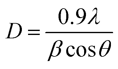
To study the effect of N ion implantation on the structural parameters such as lattice parameter, strain and crystallite size in CeO2 thin films, XRD measurements were carried out at room temperature. The XRD pattern of P and N ion implanted films are shown in Fig. 1. The sharp peaks are observed at the diffraction planes (111), (200), (220) and (311). These peaks match well with JCPDS card no. 75-0390 corresponding to the FCC fluorite structure of CeO2 lattice. The intensity of prominent peak at 28.38° i.e., (111) plane of N ion implanted films is significant and FWHM decreases with increasing ion fluences compared to the P film. The increasing intensity in XRD peak signifies an improvement in crystalline nature of CeO2 films with N ion implantation. The average crystallite size of the CeO2 is estimated from most prominent peak corresponding to (111) reflection plane using the Scherrer's formula29 and listed in Table 1,| |
 | (1) |
where D is the crystallite size, λ (1.54 Å) is wavelength of X-ray, β is FWHM and θ is Bragg's diffraction angle. The calculated data is shown in Table 1. The dislocation density ‘δ’ which is total length of dislocation lines per unit volume is measured using δ = 1/D2.30 The dislocation density is found to decrease with ion fluences as given in Table 1. This decrease in the dislocation density corresponds to reduction of the disorder with increasing N ion fluence inside CeO2 films. Furthermore, the lattice parameter of CeO2 thin films is measured using the following expression,31| |
 | (2) |
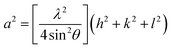
where a is lattice constant for FCC structure of CeO2. The lattice parameter of P film (5.441 Å) is found larger than the bulk CeO2, (5.411 Å) (JCPDS card no. 75-0390). It is also observed that lattice parameter of N1E15 film is higher compared to N1E16 and N6E16 films. This suggests that at lower concentration of N ions, these are likely to occupy O sites. It may be noted that the ionic radius of N (1.71 Å) ion is slightly larger than that of O (1.40 Å). Hence, this is likely to change in lattice parameter and create lattice strain which in turn affects various physical properties of CeO2 thin films. The strain ‘ε’ is estimated using Williamson–Hall (W–H) analysis,32 as shown in Fig. 2. The graphs were plotted between 4![[thin space (1/6-em)]](https://www.rsc.org/images/entities/char_2009.gif) sin(θ) (x-axis) and βcos(θ)/λ (y-axis). The slope of the linear fitted data corresponds to strain in the sample and listed in Table 1. The strain is found to be maximum for the P film and reduces with N ion fluence in the films. This indicates strain relaxation in the films after N ion implantation. The positive value of strain ‘ε’ corresponds to tensile strain in CeO2 thin films.
sin(θ) (x-axis) and βcos(θ)/λ (y-axis). The slope of the linear fitted data corresponds to strain in the sample and listed in Table 1. The strain is found to be maximum for the P film and reduces with N ion fluence in the films. This indicates strain relaxation in the films after N ion implantation. The positive value of strain ‘ε’ corresponds to tensile strain in CeO2 thin films.
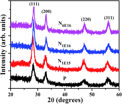 |
| | Fig. 1 XRD patterns of P and N ion implanted CeO2 thin films. | |
Table 1 Structural and morphological parameters of P and N ion implanted CeO2 thin films. The crystallite size, lattice parameter, strain and dislocation density were obtained from XRD while roughness and particle size from AFM
| Ion fluence (ions per cm2) |
Crystallite size (nm) |
Lattice parameter (Å) |
Strain (ε) × 10−2 |
Roughness (nm) |
Dislocation density, δ × 1012 (m−2) |
Particle size (nm) |
| P |
8.0 |
5.441 |
7.11 |
3.20 |
1.547 |
59.4 |
| N1E15 |
8.7 |
5.462 |
6.41 |
2.62 |
1.327 |
60.2 |
| N1E16 |
10.8 |
5.421 |
6.34 |
2.61 |
0.853 |
61.3 |
| N6E16 |
11.8 |
5.417 |
3.15 |
2.56 |
0.718 |
81.7 |
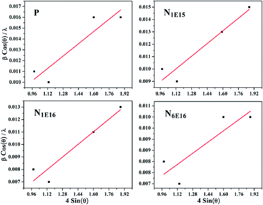 |
| | Fig. 2 W–H plot of P and N ion implanted CeO2 thin films. | |
3.2 Rutherford backscattering (RBS) spectrometry
In order to confirm the composition and thickness of the deposited films, RBS measurement was performed and then simulated with XRUMP software (Fig. 3). The simulated spectra show that the average thickness of the films are ∼300 to 320 nm and the Ce:O ratio is 1:2. It is evident from Fig. 3 that N is detected for the highest fluence film (N6E16). However, for lower fluences (N1E15 and N1E16) implanted films, the signal from N in RBS was very weak because of low concentrations. Further, to confirm the depth and the distribution of N ions in CeO2 thin films the TRIM calculations were carried out using SRIM software. From the Fig. 4, the depth of N ions in CeO2 thin films is found to be ∼110 nm and the distribution is Gaussian in nature. The observed depth of N ions inside CeO2 thin film is consistent with the simulation of the RBS data using XRUMP software.
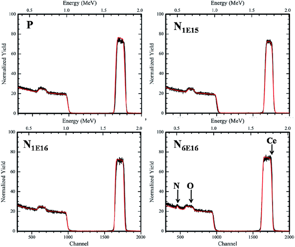 |
| | Fig. 3 Simulated RBS spectra of P and N ion implanted CeO2 thin films. | |
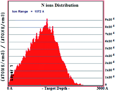 |
| | Fig. 4 Depth distribution of 80 keV N ions in CeO2 thin film. | |
3.3 Atomic Force Microscopy (AFM)
Fig. 5 shows AFM images of P and N ion implanted CeO2 films. The formation of closely packed circular shaped nanoparticles on the surface of the films is clearly observed. It is evident that nanoparticles are well grown on the surface of the films and are uniformly distributed on 2 × 2 μm2 scan area of the films. However, the surface morphology of N6E16 is slightly different from the P, N1E15 and N1E16 films indicating the effect of higher energy deposition at higher fluence of N ions. The smaller particles are agglomerated on the surface of N6E16 film. The average particle size and root mean square (RMS) surface roughness values of P, N1E15, N1E16 and N6E16 films are given in Table 1. It is observed that the surface roughness decreases with N ion implantation. The variation in particle sizes for P film and N ion implanted CeO2 thin films obtained from AFM are found to be consistent with the crystallite sizes of XRD (see in Table 1).
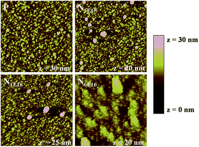 |
| | Fig. 5 AFM images (size: 2 × 2 μm2) of P and N ion implanted CeO2 thin films. | |
3.4 Raman spectroscopy
Raman spectroscopy provides the structural and additional details like defects created in the materials. Fig. 6 shows the Raman spectra of all the thin films investigated in this study. The prominent peak at ∼443 to 463 cm−1 is ascribed to Raman-active vibrational mode (F2g) of CeO2, which arises due to symmetrical stretching mode of O anions around Ce cations (O–Ce–O).33 The Raman spectra of implanted films show small shift in F2g mode towards higher wavelength and broadening in FWHM with ion fluence. Presence of inhomogeneous strain and defects contribute to the structural changes in the Raman spectra.34 It is also evident that the intensity of F2g mode enhances upto N1E16 ion fluence and the intensity decreases for N6E16 film. Besides, the prominent peak (F2g) mode in N ion implanted CeO2 thin films show additional peaks at about 620 cm−1 and 670 cm−1. The peak positioned at ∼620 cm−1 is attributed to intrinsic VO that arise to the reduction of Ce4+ to Ce3+ ions. This indicates that O sublattice is affected as a result of change in grain size and doping.35 However, the peak appears at around 670 cm−1 might be attributed to second-order Raman transition of CeO2.36 Further, the intensity of intrinsic VO mode at about 620 cm−1 and second-order Raman transition about 670 cm−1 in CeO2 films suppresses for higher N ion fluences (i.e., N1E16 and N6E16).
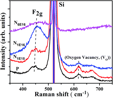 |
| | Fig. 6 Raman spectra of P and N ion implanted CeO2 thin films. | |
3.5 UV-visible analysis
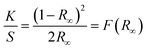
To determine the band gap energies of P and N ion implanted thin films, the Kubelka–Munk (KM) equation was employed which is given as,26| |
 | (3) |
where K, S, R∞ and F(R∞) are known as KM absorption coefficient, KM scattering coefficient, R∞ = Rsample/Rstandard and KM function respectively. The direct band gap of the semiconductor can be evaluated using the following equation,37where, α is so called linear absorption coefficient of the material, C1 is a constant of proportionality and hv corresponds to photon energy. Using the KM function in eqn (4) following expression can be obtained,| | |
[F(R∞)hv]2 = C2(hv − Eg)1/2
| (5) |
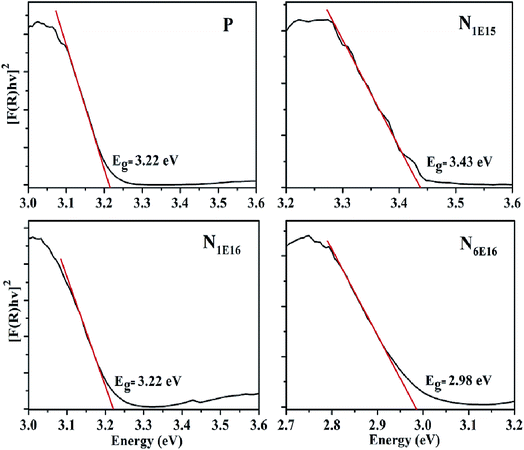
Therefore, computing F(R∞) from eqn (3) and plotting [F(R∞)hv]2 vs. hv, the band gap (Eg) of a films can be obtained.33 Fig. 7 displays the UV-vis reflectance spectra of P film and N1E15, N1E16 and N6E16 thin films. The optical band gap of P film is found to be 3.22 eV which is consistent with literature.38 It is observed that the band gap initially increases for N1E15 film (3.43 eV) and then it decreases for higher fluences N1E16 (3.22 eV) and N6E16 (2.98 eV). The variations in band gap for N ion implanted CeO2 are found to be consistent with XRD results. As discussed in XRD section, the N occupies interstitial site for N1E16 and N6E16 films compared with substitutional site for N1E15 film. Thus, the non-uniform distribution of N into CeO2 lattice for lower and higher fluences might be the reason behind the inconsistent change in band gap. This is also consistent with XRD and Raman data. It is believed that different kinds of defects are produced during N ion implantation. Similar results were reported by Xue et al. in optical band gaps after N ion implantation.39
 |
| | Fig. 7 UV-vis reflectance of P and N ion implanted CeO2 thin films. | |
3.6 Photoluminescence studies
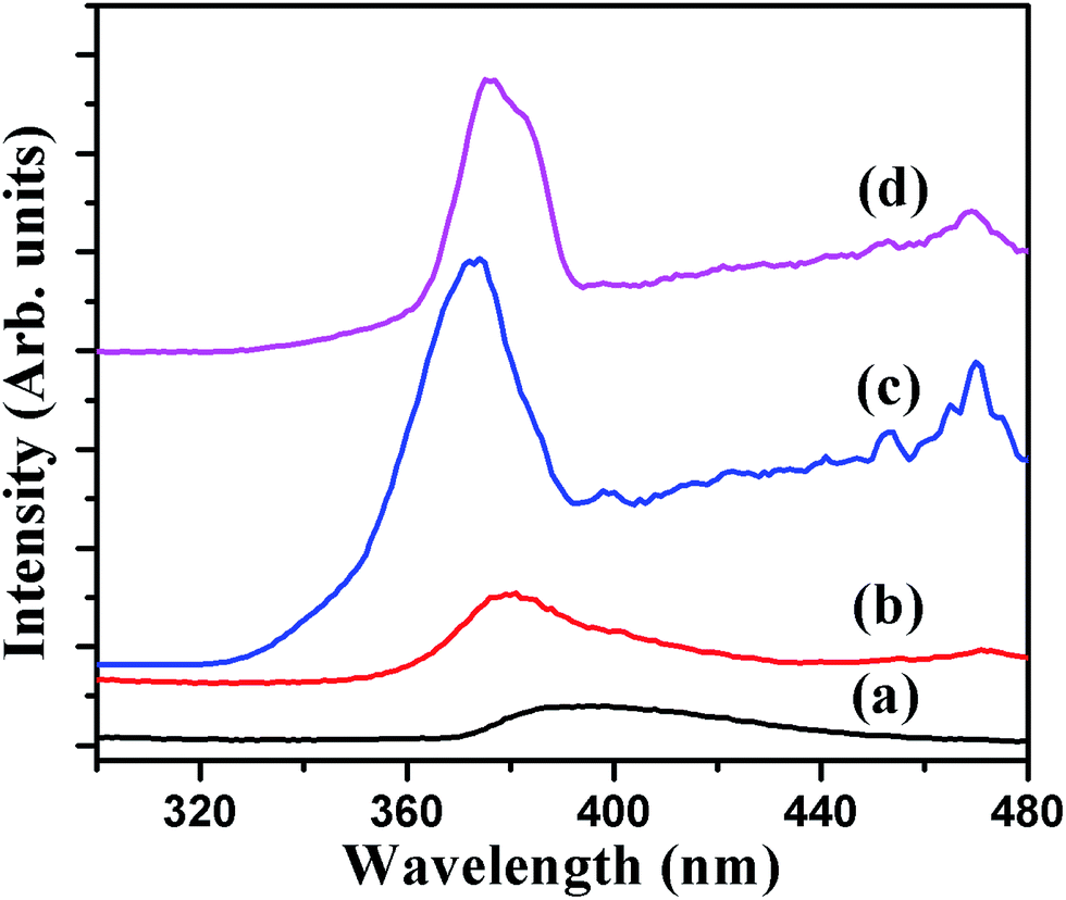
The room-temperature PL spectra of the P and N ion implanted CeO2 thin films measured using 280 nm excitation wavelength are shown in Fig. 8. The PL spectra exhibit wide emission band ∼395 nm (∼3.13 eV) for P film and sharp emission bands for N ion implanted films ∼370 nm. The strong UV emission for P and N1E15, N1E16 and N6E16 films indicate that optical band gap changes with N ion implantation. Based on this PL study, the emission bands lying between 365–400 nm for CeO2 thin films are ascribed to the charge transfer from Ce 4f to O 2p band due to different defect levels.40,41 The weak bands at 400, 460 and 470 nm are found for N ion implanted films. The observed band gap results are consistent with UV-vis spectroscopic results. It is suggested that the strong emission ∼369 nm for CeO2 is attributed to the defects like dislocations or O defects supporting for prompt O mobility.40,41
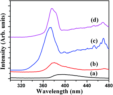 |
| | Fig. 8 Room-temperature PL spectra of P and N ion implanted CeO2 thin films: (a) P, (b) N1E15, (c) N1E16, and (d) N6E16. | |
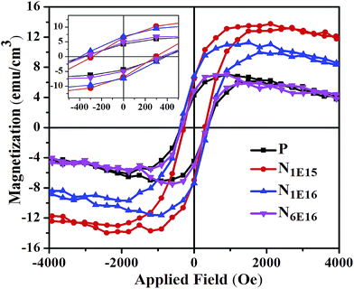
3.7 Magnetic measurements
Fig. 9 shows the magnetization (M) vs. applied magnetic field (H) dependence for P and N ion implanted CeO2 thin films. Inset in Fig. 9 displays the coercivity of P film and N ion implanted CeO2 thin films. It is evident that the values of saturation magnetization and coercivity are higher for N ion implanted films compared with P. Usually, pure CeO2 exhibits diamagnetic behaviour.42 However, the presence of defects such as VO charge imbalance and the nanosized effects are possible causes for FM in CeO2.43 It was proposed by Novica et al. that surface of nanoparticles plays a crucial role in RTFM which is an intrinsic property of nanocrystalline CeO2.42 The experimental and theoretical reports suggest that VO plays an important role in establishing FM in nanosized CeO2 and there exist a strong correlation between VO and the saturation magnetization.44,45 Ge et al. proposed that spin polarization of 4f-shell electrons of Ce ions around VO cause net magnetic moment for pure CeO2.45 It is accepted that the F-center exchange mechanism is suitable to explain the ferromagnetic ordering in nanosized CeO2.46 In accordance to this, VO (F-center) traps an electron which acts as a coupling agent between magnetic Ce3+ ions resulting in the formation of overlapped magnetic polarons. There are three possible charge states for the VO: (a) when no electron is trapped in VO, called F2+ center, (b) when one electron is trapped in VO which can mediate ferromagnetic ordering known as F+ center, and (c) when two electrons are trapped in VO and show singlet (S = 0) state which mediates weak antiferromagnetic ordering known as F0 center.47,48 It is predicted from theoretical calculation that VO moves from nanoparticles interior to surface.49 Previous reports suggest that surface layers play a significant role in the establishment of FM compared with interior of sample.50 The substitution of N impurities near the vacancies may lead to form defect complexes which strongly affect the RTFM in MgO samples.24 It is clearly seen from the Fig. 9 that P and N ion implanted films show hysteresis loops which indicate RTFM in CeO2 films. The observed RTFM for pristine CeO2 film might be recognized due to the presence of VO. It is established from the XRD results that N occupies the O site in the host CeO2 lattice. The inclusion of trivalent N ion at divalent O site generates excess charges which are compensated through the introduction of VO. Therefore, the incorporation of N ion (N1E15) into the host CeO2 lattice gives rise to increase in saturation magnetization up to a particular N concentration. This increase in VO or O-related defects might be responsible for enhancement of saturation magnetisation in the N1E15 film. However, at higher fluence (i.e. N1E16 and N6E16), the N ions are distributed non-uniformly and occupy some interstitial sites as confirmed by XRD measurement. Incorporation of N ions at interstitial sites results in the suppression of magnetic moment and hence reduction in RTFM. The decrease in saturation magnetization with further increase in N ion fluence is correlated with decreasing VO. The increasing VO or defects at low fluence (N1E15) and decreasing VO with further increase in N ion fluence compared with P is clearly evident from the Raman spectra (see Fig. 6). These observed results are in well agreement with C implanted ZnO thin films.15
 |
| | Fig. 9 Room temperature M − H plot of P film and N ion implanted CeO2 thin films. | |
Based on density functional theory (DFT) calculations, Valentin et al. suggested that N doping in anatase TiO2 reduces the energy required for the formation of VO in bulk form.51 It is easy to reduce the pure rutile TiO2 than anatase TiO2. This phase also favours the presence of substitutional N.52 Furthermore, it is reported that in case of rutile phase, the energy required for the formation of vacancy reduces from 4.3 to 1.0 eV whereas for substitution of O with N from 9.7 to 6.4 eV.51 As 2p orbital of N2− occupies one electron less than O, the binding energy of the 2p bonding electrons is lower compared with the O ion.14 In this way, the one electron state of N2− ion will have larger orbital radius as compared to an isolated ion. At a suitable N concentration, the corresponding orbitals of the nearest defects will overlap, giving rise to a narrow impurity band with one hole per N ion leading to magnetic moment. For the two holes in 2p orbitals of O or N ions have lowest configurations that exhibit spin triplet state corresponding to the existence of an associated magnetic moment.14 The overlapping between the defect states and the formation of a defect band may result in magnetic clusters and hence lead to induce RTFM in N ion implanted CeO2 thin films. The interstitial occurrence of N ions suppresses the magnetic moments which result in the reduction of RTFM. The effect of C dopant on the magnetic properties of ZnO thin films has been studied theoretically as well as experimentally.15 Pan et al. proposed experimentally as well as based on theoretical calculations (DFT) that the saturation magnetization increases for low carbon concentrations (from 0 to 1 at%). However, it decreases when C concentration reaches about 5 at% in the sample.53 Zhou et al. also investigated experimentally the effect of C concentration (at%) over magnetization and showed that the saturation magnetization is highest at C concentration ∼2 at% whereas it reduced with higher concentration of C.54 It has been suggested that the non-uniform distribution of C atoms at higher concentrations may be the reason. Based on theoretical studies, Ye et al. reported that the increase in the C content results in decrease in the separation among C–C ions favouring dominance of antiferromagnetic in the host lattice over the FM nature at higher concentration.55 Based on these results, it is interpreted that strength of the exchange coupling is directly correlated with the separation between the C–C atoms. On the basis of above findings, in the present case the N ions are distributed non-uniformly inside host CeO2 lattice at higher N fluences (N1E16 and N6E16). This is consistent with the findings of Kumar et al.15 We have also observed that the maximum saturation magnetization is achieved at lower N concentration i.e., 0.14% and decreases for the higher N ion concentrations (1.4% and 8.4%). In context of these calculations and observed experimental results, it is realized that the distribution of N inside the host CeO2 lattice plays a significant role to modify the magnetic properties. The modification in the magnetic properties by N ion implantation provides an evidence for creating DMO material based spintronics.
4. Conclusions
The structural, morphological, optical and magnetic properties of N implanted CeO2 thin films were investigated. The XRD confirmed the FCC structure corresponding to CeO2, and the Raman results show the presence of defects such as oxygen vacancies in these thin films. The band gap of CeO2 film was found to be ∼3.22 eV which is consistent with previous reports. RBS measurement confirms the presence of N ions in the CeO2 films. The RTFM was observed in the pristine CeO2 and an enhancement in saturation magnetization and residual magnetization for low fluence N ion implanted CeO2 thin film. These changes are attributed to the creation of VO due to N replacing O in CeO2 lattice. A possible mechanism, the F-center exchange mechanism, is discussed to understand the FM ordering in these films. It is proposed that the distribution of N ions inside the host CeO2 lattice plays a significant role to modify the magnetic properties.
Acknowledgements
One of the authors, Pawan Kumar, is thankful to the CSIR, New Delhi for providing the SRF fellowship. He also gratefully acknowledges the support and encouragement received from Inter University Accelerator Centre, New Delhi, India.
References
- P. Singh, K. M. K. Srivatsa and S. Das, Adv. Mater. Lett., 2015, 6, 371–376 CrossRef CAS.
- A. Thurber, K. M. Reddy, V. Shutthanandan, M. H. Engelhard, C. Wang, J. Hays and A. Punnoose, Phys. Rev. B: Condens. Matter Mater. Phys., 2007, 76, 165206 CrossRef.
- A. Sharma, M. Varshney, H. J. Shin, Y. J. Park, M. G. Kim, T. K. Ha, K. H. Chae and S. Gautam, Phys. Chem. Chem. Phys., 2014, 16, 19909 RSC.
- M. Venkatesan, C. B. Fitzgerald and J. M. D. Coey, Nature, 2004, 430, 630 CrossRef CAS PubMed.
- N. H. Hong, J. Sakai, N. Poirot and V. Brize, Phys. Rev. B: Condens. Matter Mater. Phys., 2006, 73, 132404 CrossRef.
- M. I. B. Bernardi, A. Mesquita, F. Béron, K. R. Pirota, A. O. de Zevallos, A. C. Doriguettod and H. B. de Carvalho, Phys. Chem. Chem. Phys., 2015, 17, 3072–3080 RSC.
- J. C. Bear, P. D. McNaughter, P. Southern, P. O'Brien and C. W. Dunnill, Crystals, 2015, 5, 312–326 CrossRef CAS.
- T. Dietl, H. Ohno, F. Matsukura, J. Cibert and D. Ferrand, Science, 2000, 287, 1019–1022 CrossRef CAS PubMed.
- X. P. Han, J. Lee and H. I. Yoo, Phys. Rev. B: Condens. Matter Mater. Phys., 2009, 79, 100403 CrossRef.
- M. Y. Ge, H. Wang, E. Z. Liu, J. F. Liu, J. Z. Jiang, Y. K. Li, Z. A. Xu and H. Y. Li, Appl. Phys. Lett., 2008, 93, 062505 CrossRef.
- J. M. D. Coey, A. P. Douvalis, C. B. Fitzgerald and M. Vankatesan, Appl. Phys. Lett., 2004, 84, 1332–1334 CrossRef CAS.
- Y. L. Liu, Z. Lockman, A. Aziz and J. MacManus-Driscoll, J. Phys.: Condens. Matter, 2008, 20, 165201 CrossRef.
- K. S. Ranjith, P. Saravanan, S. H. Chen, C. L. Dong, C. L. Chen, S. Y. Chen, K. Asokan and R. T. Rajendrakumar, J. Phys. Chem. C, 2014, 118, 27039–27047 CAS.
- M. M. Cruz, R. C. da Silva, N. Franco and M. Godinho, J. Phys.: Condens. Matter, 2009, 21, 206002 CrossRef CAS PubMed.
- P. Kumar, H. Malik and K. Asokan, EPL, 2015, 110, 67006 CrossRef.
- H. Pan, J. B. Yi, L. Shen, R. Q. Wu, J. H. Yang, J. Y. Lin, Y. P. Feng, J. Ding, L. H. Van and J. H. Yin, Phys. Rev. Lett., 2007, 99, 127201 CrossRef CAS PubMed.
- I. S. Elfimov, A. Rusydi, S. I. Csiszar, Z. Hu, H. H. Hsieh, H. J. Lin, C. T. Chen, R. Liang and G. A. Sawatzky, Phys. Rev. Lett., 2007, 98, 137202 CrossRef CAS PubMed.
- P. Kumar, V. Sharma, A. Sarwa, A. Kumar, S. Surbhi, R. Goyal, K. Sachdev, S. Annapoorni, K. Asokan and D. Kanjilal, RSC Adv., 2016, 6, 89242 RSC.
- H. Pan, J. B. Yi, L. Shen, R. Q. Wu, J. H. Yang, J. Y. Lin, Y. P. Feng, J. Ding, L. H. Van and J. H. Yin, Phys. Rev. Lett., 2007, 99, 127201 CrossRef CAS PubMed.
- L. C. Ming, G. H. Quan, X. Xia, Z. Yan, J. Yong, C. Men and Z. X. Tao, Chin. Phys. B, 2011, 20, 047505 CrossRef.
- G. D. Liu, S. L. Ji, L. L. Yin, G. T. Fei and C. H. Ye, J. Phys.: Condens. Matter, 2010, 22, 046002 CrossRef PubMed.
- M. Kapilashrami, J. Xu, K. V. Rao, L. Belova, E. Carlegrim and M. Fahlman, J. Phys.: Condens. Matter, 2010, 22, 345004 CrossRef PubMed.
- B. M. Maoz, E. Tirosh, M. B. Sadan and G. Markovich, Phys. Rev. B: Condens. Matter Mater. Phys., 2011, 83, 161201 CrossRef.
- Q. Li, B. Ye, Y. Hao, J. Liu, W. Kong and B. Ye, Nucl. Instrum. Methods Phys. Res., Sect. B, 2013, 297, 29–34 CrossRef CAS.
- S. Zhou, Q. Xu, K. Potzger, G. Talut, R. Grötzschel, J. Fassbender, M. Vinnichenko, J. Grenzer, M. Helm, H. Hochmuth, M. Lorenz, M. Grundmann and H. Schmidt, Appl. Phys. Lett., 2008, 93, 232507 CrossRef.
- R. Kumari, A. Sahai and N. Goswami, Prog. Nat. Sci.: Mater. Int., 2015, 25, 300–309 CrossRef CAS.
- L. Yiwei, Z. Qingfeng and L. Run-Wei, Chin. Phys. B, 2013, 22, 127502 CrossRef.
- B. Cord, W. Maass, J. Schroeder, K.-H. Schuller and U. Patz, Thin Solid Films, 1989, 175, 287–293 CrossRef CAS.
- P. Kumar, P. Kumar, A. Kumar, R. C. Meena, R. Tomar, F. Chand and K. Asokan, J. Alloys Compd., 2016, 672, 543–548 CrossRef CAS.
- D. P. Padiyan, A. Marikani and K. R. Murali, Mater. Chem. Phys., 2003, 78, 51 CrossRef.
- R. K. Hailstone, A. G. DiFrancesco, J. G. Leong, T. D. Allston and K. J. Reed, J. Phys. Chem. C, 2009, 113, 15155–15159 CAS.
- R. Abaira, T. Dammak, A. Matoussi and A. Younes, Superlattices Microstruct., 2016, 91, 365–374 CrossRef CAS.
- P. C. A. Brito, D. A. A. Santos, J. G. S. Duque and M. A. M. Macedo, Phys. B, 2010, 405, 1821–1825 CrossRef CAS.
- Z. V. Popovic, Z. D. Mitrovic, M. Scepanovic, M. G. C. Brojcin and S. Askrabic, Ann. Phys., 2011, 523, 62–74 CrossRef CAS.
- S. Phokha, S. Pinitsoontorn and S. Maensiri, Nano-Micro Lett., 2013, 5, 223–233 CrossRef CAS.
- S. Dogra, N. D. Sharma, J. Singh, H. K. Poswal, S. M. Sharma and A. K. Bandyopadhyay, High Press. Res., 2011, 31, 292–303 CrossRef CAS.
- J. I. Pankove, Optical Processes in Semiconductors, Courier Corporation, 2012 Search PubMed.
- S. A. Ansari, M. M. Khan, M. O. Ansari, S. Kalathil, J. Lee and M. H. Cho, RSC Adv., 2014, 4, 16782 RSC.
- S. W. Xue, L. X. Shao and J. Zhang, Journal of Optoelectronic and Biomedical Materials, 2009, 1, 34–41 Search PubMed.
- P. Goel, M. Arora and A. M. Biradar, RSC Adv., 2014, 4, 11351 RSC.
- G. Wang, Q. Mu, T. Chen and Y. Wang, J. Alloys Compd., 2010, 493, 202–207 CrossRef CAS.
- N. Paunovi, Z. D. Mitrovi, R. Scurtu, S. Askrabic, M. Prekajski, B. Matovic and Z. V. Popovic, Nanoscale, 2012, 4, 5469 RSC.
- M. Varshney, A. Sharma and H. J. Shin, Adv. Sci., Eng. Med., 2015, 15, 1–7 Search PubMed.
- A. Sundaresan and C. N. R. Rao, Nano Today, 2009, 4, 96–106 CrossRef CAS.
- V. Fernandes, P. Schio, A. J. A. deOliveira, W. A. Ortiz, P. Fichtner, L. Amaral, I. L. Graff, J. Varalda, N. Mattoso, W. H. Schreiner and D. H. Mosca, J. Phys.: Condens. Matter, 2010, 22, 216004 CrossRef CAS PubMed.
- R. K. Singhal, P. Kumari, A. Samariya, S. Kumar, S. C. Sharma, Y. T. Xing and E. B. Saitovitch, Appl. Phys. Lett., 2010, 97, 172503 CrossRef.
- L. R. Shah, A. Bakhtyar, Z. Hao, W. G. Wang, Y. Q. Song, H. W. Zhang, S. I. Shah and J. Q. Xiao, J. Phys.: Condens. Matter, 2009, 21, 486004 CrossRef PubMed.
- J. M. D. Coey, M. Venkatesan and C. B. Fitzgerald, Nat. Mater., 2005, 4, 173–179 CrossRef CAS PubMed.
- J. C. Conesa, Surf. Sci., 1995, 339, 337–352 CrossRef CAS.
- X. Chen, L. Guangshe, S. Yiguo, Q. Xiaoqing, L. Liping and Z. Zhigang, Nanotechnology, 2009, 20, 115606 CrossRef PubMed.
- C. D. Valentin, G. Pacchioni, A. Selloni, S. Livraghi and E. Giamello, J. Phys. Chem. B, 2005, 109, 11414 CrossRef PubMed.
- A. Bouzoubaa, A. Markovits, M. Calatayud and C. Minot, Surf. Sci., 2005, 583, 107 CrossRef CAS.
- H. Pan, J. B. Yi, L. Shen, R. Q. Wu, J. H. Yang, J. Y. Lin, Y. P. Feng, J. Ding, L. H. Van and J. H. Yin, Phys. Rev. Lett., 2007, 99, 127201 CrossRef CAS PubMed.
- S. Zhou, Q. Xu, K. Potzger, G. Talut, R. Grotzschel, J. Fassbender, M. Vinnichenko, J. Grenzer, M. Helm, H. Hochmuth, M. Lorenz, M. Grundmann and H. Schmidt, Appl. Phys. Lett., 2008, 93, 232507 CrossRef.
- X. J. Ye, C. S. Liu, W. Zhong, H. A. Song, C. T. Au and Y. W. Du, Phys. Lett. A, 2010, 374, 496 CrossRef CAS.
|
| This journal is © The Royal Society of Chemistry 2017 |
Click here to see how this site uses Cookies. View our privacy policy here. 
 Open Access Article
 This Open Access Article is licensed under a