
Phase separation and electrical performance of bithienopyrroledione polymer semiconductors embedded in insulating polymers†
Linjing
Tang‡
a,
Pan
He‡
ab,
Xiaolan
Qiao
a,
Qun
Qian
*b and
Hongxiang
Li
 *a
*a
aKey Laboratory of Synthetic and Self-Assembly Chemistry for Organic Functional Molecules, Shanghai Institute of Organic Chemistry, Chinese Academy of Sciences, 345 Lingling Road, Shanghai 200032, China. E-mail: lhx@mail.sioc.ac.cn
bDepartment of Chemistry, Shanghai University, 99 Shangda Road, Shanghai 200444, China. E-mail: qianqun@shu.edu.cn
First published on 7th August 2017
Abstract
Bithienopyrroledione (1,1′-bithieno[3,4-c]pyrrole-4,4′,6,6′-tetraone (bi-TPD)) based copolymer P1 was synthesized and characterized. Its phase separation characteristics in a P1/PMMA blend were investigated. It was found that P1 formed microsized fibers in the P1/PMMA blend and dispersed into the whole blend system. Thin film field-effect transistors using P1 films and P1/PMMA blend films as active layers were fabricated. Both devices showed p-type charge carrier transport properties under ambient conditions and ambipolar charge carrier transport behavior in a N2 atmosphere. Under ambient conditions, the P1 film transistors displayed a hole mobility of 0.48 cm2 V−1 s−1, and the blend film devices exhibited comparable performance with a hole mobility of 0.32 cm2 V−1 s−1. In a N2 atmosphere, the performance of the blend film transistors was largely improved compared with that of the P1 film ones. The hole/electron mobilities were 0.10/0.05 cm2 V−1 s−1 for the blend film transistors and 0.02/0.002 cm2 V−1 s−1 for the P1 film devices. All these results demonstrate the potential applications of bi-TPD based polymer semiconductors in high performance blend film transistors.
Introduction
Polymer transistors have attracted great attention because of their wide application and technical advantages of being fabricated on large area and flexible substrates with low cost.1 Polymer transistors consist of gate, source and drain electrodes, a dielectric layer and a polymer semiconductor layer. As the key component, the semiconductor layer is usually composed of highly pure polymer semiconductors. Recently, polymer semiconductor/insulating polymer blends have been used as semiconductor layers.2–8 The blend semiconductor layer can combine the electrical properties of polymer semiconductors with the low cost and excellent mechanical properties of insulating polymers.3,8 However the presence of insulating polymers tends to lower the device performance,4,9 and high performance polymer transistors with a blend semiconductor layer are rare. To overcome this drawback, polymer semiconductors used in the blend should (i) have excellent charge-carrier transport properties and (ii) form suitable phase-separated structures in the blend.5 Though many high performance polymer semiconductors have been reported, currently it is still a great challenge to control the phase-separated structure of polymer semiconductors because of their complicated self-assembly process in polymer blends.10 Therefore, it is difficult and important to develop new types of high performance blend film transistors.Donor–acceptor (D–A) type conjugated copolymers have captured tremendous interest as semiconductor candidates for solution-processed polymer thin-film transistors.1,11–13 Bithienopyrroledione (1,1′-bithieno[3,4-c]pyrrole-4,4′,6,6′-tetraone, bi-TPD), as a derivative of a well-known acceptor unit thieno[3,4-c]pyrrole-4,6-dione (TPD), has a planar structure and exhibits stronger electron-withdrawing properties than TPD,14 suggesting its potential applications as an electron-withdrawing unit in high performance polymer semiconductors. Compared with the well-known acceptor units (such as DPP and NDI), bi-TPD based D–A polymers are rarely reported though some of them exhibited excellent transistor performance.15 In this manuscript, bi-TPD based copolymer P1 was synthesized and characterized. Its phase-separated structure and electric performance in P1/PMMA blends were investigated. Experimental results showed that P1 formed microsized fibers and dispersed into the whole blend film. The blend film transistors displayed higher ambipolar mobility than the non-blend ones in a N2 atmosphere, demonstrating the potential applications of bi-TPD based polymers in high performance blend film transistors.
Results and discussion
Synthesis and characterization
The chemical structure and synthetic route of P1 is shown in Scheme 1. P1 was synthesized through conventional Stille coupling of dibrominated bi-TPD (compound 1) with the corresponding bis-stannylated benzo[1,2-b:4,5-b′]dithiophene (compound 2) in toluene. The crude polymer was ultimately purified by precipitation into methanol followed by successive Soxhlet extractions with organic solvents. Its number-average molecular weight (Mn) was measured by high temperature (150 °C) gel-permeation chromatography (GPC) in 1,2,4-trichlorobenzene using polystyrene as the standard. The Mn/PDI (polydispersity index) value was 26.9 kDa/3.61.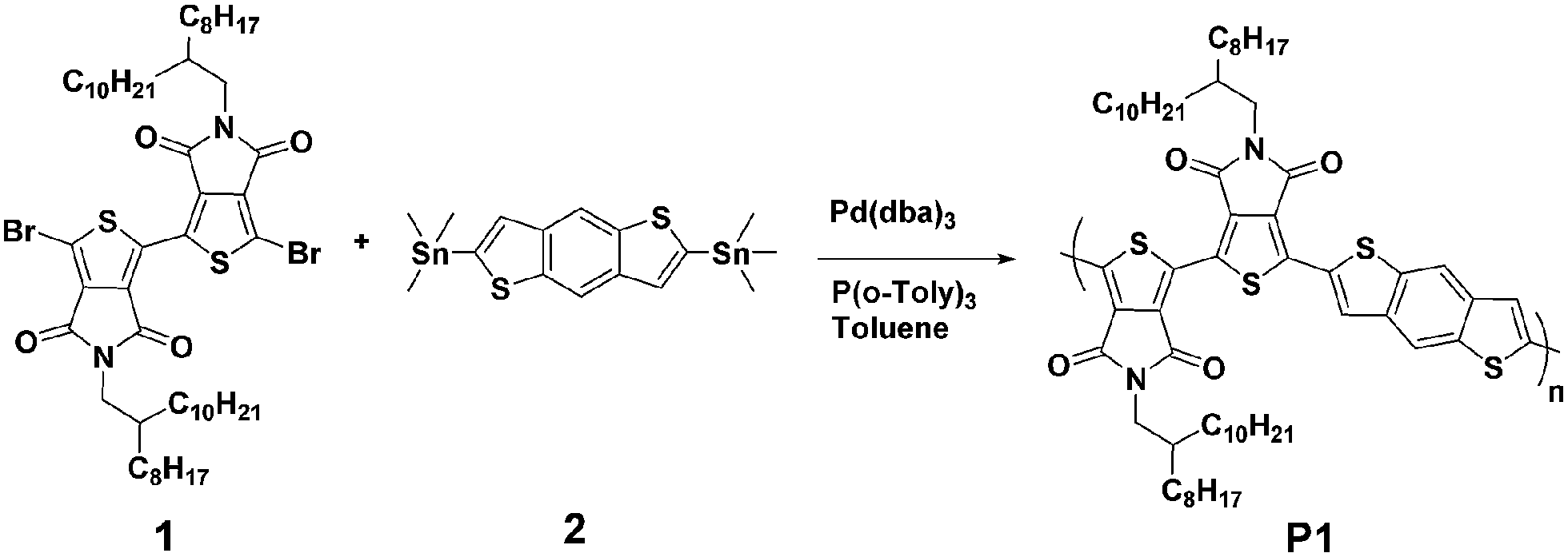 | ||
| Scheme 1 The chemical structure and synthetic route of polymer semiconductor P1. | ||
Fig. 1 illustrates the normalized absorption spectra of P1 in dilute solution (chloroform) and a thin film spin-coated on a quartz substrate. The P1 solution had absorptions in the range of 360–700 nm, and a maximum absorption peak at 588 nm together with a strong vibronic absorption shoulder peak at 544 nm were observed. Compared with that of the solution, the maximum absorption of the film was slightly red-shifted (about 14 nm). The absorption changes suggested the more planar and ordered backbone conformation of P1 in the films. The optical bandgap estimated from the onset absorption of the P1 films was 1.85 eV.
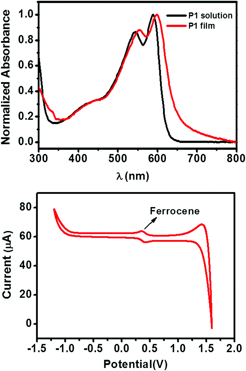 | ||
| Fig. 1 (top) The UV-vis absorption spectra of the P1 solution (in CHCl3) and thin film (quartz substrate). (bottom) The CV curve of P1 thin film. | ||
The cyclic voltammetry (CV) of the P1 films exhibited an irreversible oxidation peak (Fig. 1), which is typical for polymer semiconductors. By using the ferrocene/ferrocenium redox couple as an internal standard (the HOMO energy level of ferrocene is set at −4.8 eV with respect to the vacuum level), the HOMO energy level of P1 was calculated to be −5.61 eV. The LUMO level of P1 was −3.76 eV, which was estimated from the HOMO energy level and the optical bandgap.
Charge transport properties
The charge transport properties of P1 were studied with homo-P1 film and blend film transistors. The insulating polymer used in the blend was polymethyl methacrylate (PMMA) (Mw = 120 kg mol−1). After optimization, the concentration of P1 in the homo-solution was 2.0 mg mL−1. The blend solution was prepared by mixing 1 mL of P1 solution (10 mg mL−1 in CHCl3) with 4 mL of PMMA solution (10 mg mL−1 in CHCl3), and the concentration of P1 in the blend solution was the same as that of the homo-P1 solution. The homo-P1 and P1/PMMA blend semiconductor layers were deposited on OTS-modified SiO2 substrates with spin-coating. The device structures were in the bottom-gate, top-contact (BGTC) configuration and Au was used as source and drain electrodes. The electric characterization was carried out both under ambient conditions and in a N2 atmosphere. Fig. S2 and S3 (ESI†) show the representative transfer curves of the optimized homo-P1 film and blend film transistors measured under ambient conditions. Their device performances are summarized in Table S1 (ESI†). Both the homo-film and blend film devices exhibited typical p-channel behaviour under ambient conditions. The as-spun homo-film transistors displayed a hole mobility of 0.04 cm2 V−1 s−1. With thermal annealing, the mobility of the devices increased, and a mobility of 0.48 cm2 V−1 s−1 was observed after thermal annealing at 120 °C. The as-spun blend film devices showed a slightly higher hole mobility of 0.08 cm2 V−1 s−1. Similar to that of the homo-film ones, the performance of the blend film transistors increased with thermal annealing. The maximum mobility could reach 0.32 cm2 V−1 s−1 after thermal annealing at 160 °C.In a N2 atmosphere, both homo-film and blend film devices displayed ambipolar charge transport behaviour as evidenced by the typical V-shaped traces in the transfer curves (Fig. 2). The hole and electron mobilities of the homo-film transistors were 0.02 cm2 V−1 s−1 and 0.002 cm2 V−1 s−1 after thermal annealing at 120 °C. Compared with that of the homo-film devices, the performance of the blend film ones was remarkably improved, and the hole mobility was 0.1 cm2 V−1 s−1 and the electron mobility was 0.05 cm2 V−1 s−1. The performance changes in the homo-film devices (under ambient conditions and in a N2 atmosphere) indicated that oxygen doping occurred under ambient conditions, which is commonly observed for p-type polymer semiconductors.16–18 The comparable hole mobility of the blend film transistors under ambient conditions and in a N2 atmosphere suggested that the blend film devices have greater environmental stability.
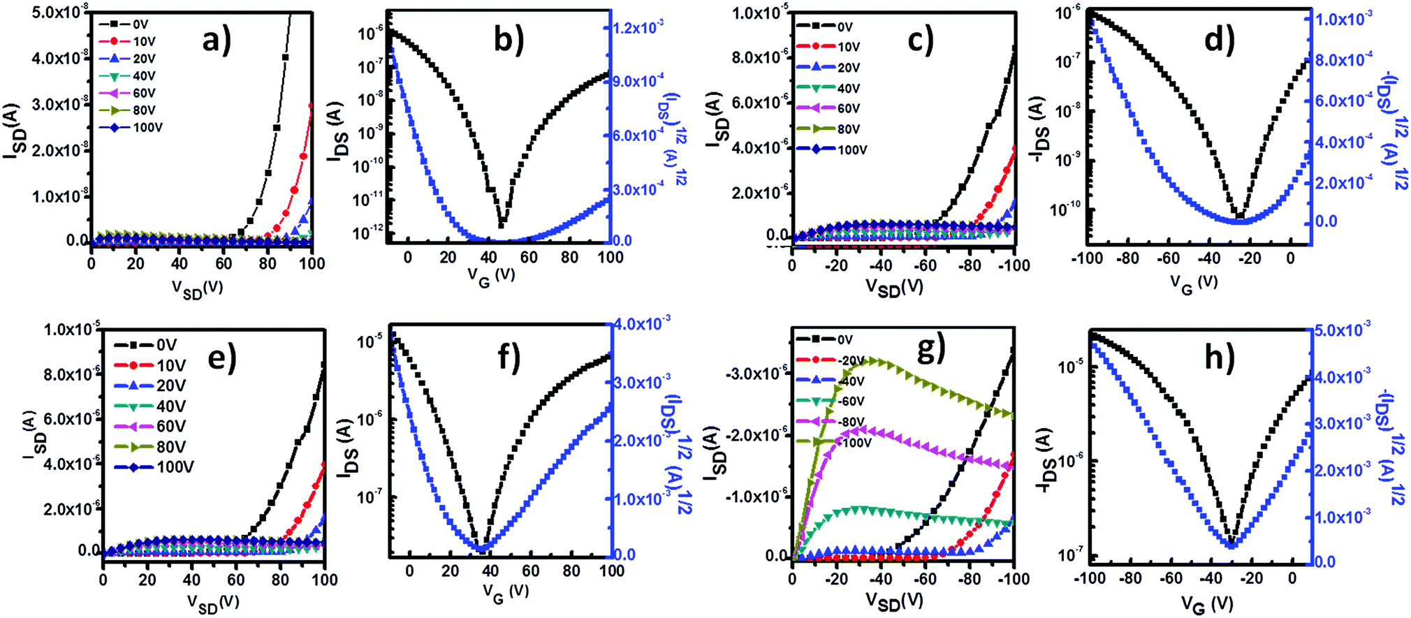 | ||
| Fig. 2 Typical transfer and output curves of BGTC transistors based on homo-P1 films and P1/PMMA blend films under N2. (a–d) Homo-P1 film transistors; (e–h) P1/PMMA blend film transistors. | ||
AFM and XRD characterization
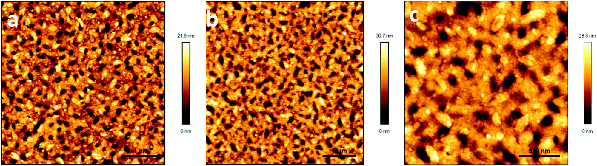
To elucidate the observed transistor performance of P1 in homo-films and blend films, we explored the morphology and structural features of these films by atomic force microscopy (AFM) and X-ray diffraction (XRD). Both films had relatively smooth morphology (Fig. 3). Fiber type microstructures were observed in the homo-film, whereas holes were observed in the blend film. The morphology of the blend film was similar to that of the homo-PMMA film spin-coated from a CHCl3 solution under the same conditions. Cho et al. reported that the morphology of the PMMA films was strongly affected by the boiling point of the solvents used.19 When a low boiling point solvent (toluene) was used, holes were observed on the film surface, and no holes were observed when a high boiling point solvent (1,2,4-trichlorobeneze) was chosen. Hence the formation of holes in the blend film should be due to the low boiling point of CHCl3. Despite the morphology defects (holes), high and balanced ambipolar performance of the blend film transistors was achieved, indicating that continuous charge carrier transport paths existed in the blend films.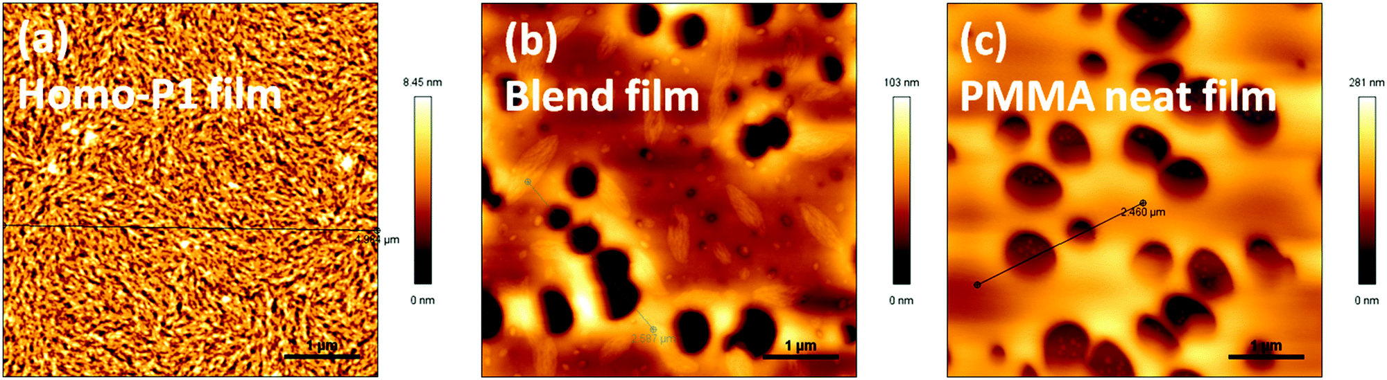 | ||
| Fig. 3 AFM height images of (a) homo-P1 films, (b) P1/PMMA blend films and (c) homo-PMMA films annealed at 120 °C. | ||
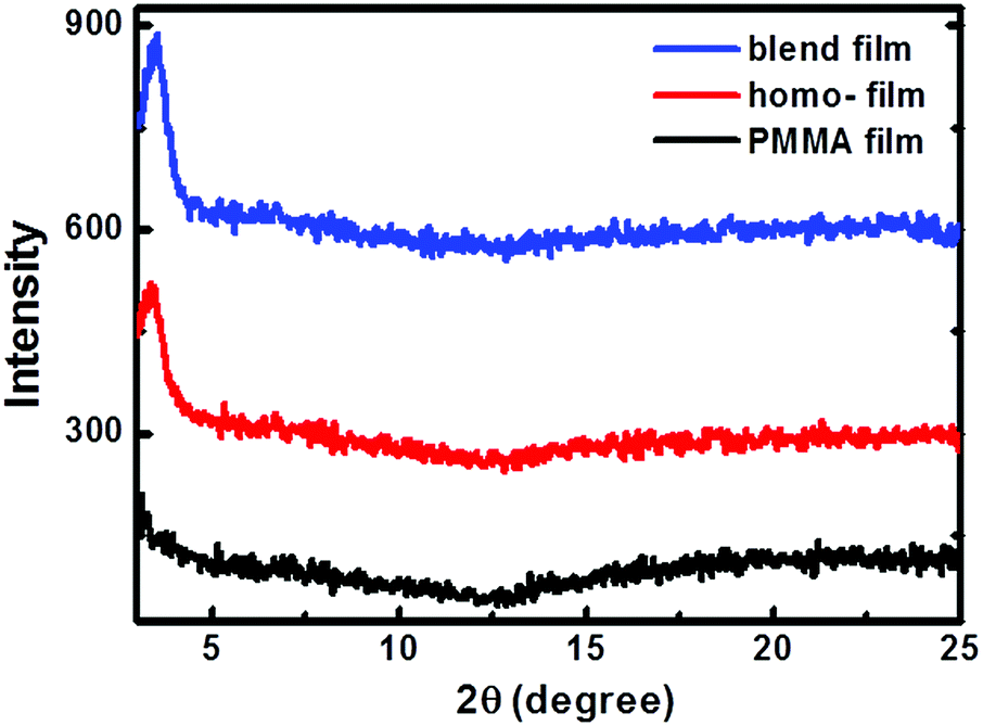
The crystallinity of the homo-P1 and P1/PMMA blend films was investigated using wide-angle out-of-plane X-ray diffraction. Fig. 4 illustrates the diffraction patterns of the homo-P1 films and blend films. For comparison, the XRD diffraction of the homo-PMMA films deposited under the same conditions was also studied. No peaks were observed for the homo-PMMA films, and the homo-P1 film showed a weak diffraction peak at 2θ = 3.61°, corresponding to a d-spacing of 24.45 Å. The blend film exhibited the same diffraction pattern as the homo-P1 film, indicating that P1 adopted the same packing structure in the blend film.
 | ||
| Fig. 4 XRD patterns of homo-P1 films, P1/PMMA blend films and homo-PMMA films annealed at 120 °C. | ||
Phase separation characterization
A suitable phase separated structure of the polymer semiconductor is a prerequisite for blend film transistors.5 There are three kinds of phase-separated structures for P1 in the blend film,4,5,20,21 (1) P1 was vertical phase-separated and at the bottom of the blend film; (2) P1 was vertical phase-separated and on the top of the PMMA layer; (3) P1 dispersed in the whole blend film.If P1 adopted the first kind of phase separated structure in the blend film, BGTC transistors would not show field-effect transistor characteristics, because of the large resistance of the PMMA layers between P1 and the source/drain electrodes. This is inconsistent with our experimental results. Moreover, the water contact angle measurements showed that the water contact angle of the blend films (97°) was similar to that of the homo-P1 films (98°), and larger than that of the homo-PMMA films (73°) (Fig. S4, ESI†), further indicating that P1 did not adopt the first kind of phase-separated structure in the blend film.
Then blend film transistors with the bottom-gate bottom-contact (BGBC) configuration were fabricated. Electrical characterization showed that these transistors displayed ambipolar behaviour with a hole mobility of 2.4 × 10⁻³ cm2 V−1 s−1 and an electron mobility of 2.5 × 10⁻³ cm2 V−1 s−1 (Fig. S5, ESI†). Similar to that of BGTC devices, the performance of the homo-film transistors with a BGBC structure (μh: 7.7 × 10⁻⁴ cm2 V−1 s−1; μe: 9.8 × 10⁻⁴ cm2 V−1 s−1) was lower than that of the blend film ones. Large contact resistance was observed for the BGBC devices (Fig. S6, ESI†), which is commonly observed in BGBC transistors and should be responsible for their lower performances, compared with that of the BGTC ones.22,23 The ambipolar character of the BGBC devices ruled out the possibility of the second kind of phase separated structure of P1 in the blend film.
To further confirm that P1 was dispersed in the whole blend film, PMMA was selectively etched by immersing the blend films in ethanol. Ethanol is a good solvent for PMMA, but does not dissolve P1. Fig. 5 illustrates the AFM images of the blend films after ethanol etching for 30 min and 12 hours. A bicontinuous fiber network of P1 and PMMA was observed after etching for 30 min. No network was peeled off from the substrate after the blend film was etched for 12 hours, which strongly supported the conclusion that P1 dispersed in the whole blend film. Please note that the homo-PMMA film totally dissolved in ethanol after it had been immersed in ethanol for 12 hours. This fiber network revealed the slight effect of surface defects (holes) on device performance. Moreover, the diameter of the fibers in the blend films largely increased compared with that of the ones in the homo-films, which should be responsible for the higher performance of the blend film transistors.
 | ||
| Fig. 5 AFM height images of P1/PMMA blend films after etching in ethanol for (a) 30 min, 5 × 5 μm, (b) 12 hours, 5 × 5 μm and (c) 12 hours, 2 × 2 μm. | ||
Conclusion
Bi-TPD based polymer semiconductor P1 was synthesized and characterized. Its charge transport properties were investigated with homo-P1 film and P1/PMMA blend film transistors. Under ambient conditions, both the homo-film and blend film transistors showed typical p-channel behaviour with comparable field-effect mobility, and the highest hole mobility could reach 0.48 cm2 V−1 s−1. In a N2 atmosphere, both devices displayed ambipolar charge carrier transport properties, and the performance of the blend film transistors highly improved, compared with that of the homo-film ones. The hole and electron mobilities of the blend film transistors were 0.1 cm2 V−1 s−1 and 0.05 cm2 V−1 s−1 respectively. Phase-separation characteristics revealed that P1 dispersed in the whole blend film and formed fiber network microstructures. All these results demonstrate the potential applications of bi-TPD based polymer semiconductors in high performance blend film transistors.Experimental section
Materials and instruments
All the chemicals and reagents were commercially available and used as received. The monomers 1 and 2 were prepared according to the established methods.15,24 Elemental analysis was conducted using an Elementar Vario EL III elemental analyzer. Mn and PDI were measured using a Polymer Laboratories GPC 220 instrument at 150 °C using standard polystyrene (PS) as the reference and 1,2,4-tricholorobenzene as the eluent at a flow rate of 1.00 mL min−1. Absorption spectra were recorded on a U-3900 UV-vis spectrophotometer. Cyclic voltammetric measurements were performed in a conventional three electrode cell using a platinum working electrode, a platinum wire counter electrode, and a saturated calomel electrode (SCE) as the reference electrode on a computer-controlled CHI610D instrument. AFM images of the homo and blend films were recorded on a JPK NanoWizard3 using tapping mode. 1D-XRD of the films along the out-of-plane direction was obtained by using a PAN Analytical X'pert Powder Diffraction System.Synthesis of P1
A reaction mixture of compound 1 (0.511 g, 0.5 mmol), compound 2 (0.258 g, 0.5 mmol), Pd2(dba)3 (0.0023 g, 0.025 mmol) and P(o-tolyl)3 (0.030 g, 0.09 mmol) in toluene (25 mL) was heated to reflux for 72 h under nitrogen. After cooling to room temperature, the reaction mixture was slowly dropped into 300 mL of methanol (containing 10 mL of concentrated HCl). The precipitate was filtered and extracted using Soxhlet apparatus with methanol, acetone, petroleum ether and dichloromethane. The dichloromethane solution was concentrated by evaporation to about 20 mL and was poured into 200 mL of methanol. The precipitate was collected by filtration and dried under vacuum to afford P1 (0.426 g, yield: 80%). Mn: 26.9 kDa, PDI: 3.61. Anal. calcd for (C62H86N2O4S4)n: C, 70.78; H, 8.18; N, 2.66%; found: C, 70.68; H, 8.42; N, 2.66%.Device fabrication and characterization
Heavily doped silicon and SiO2 were used as the gate electrode and dielectric. SiO2 was treated with OTS according to a previously reported procedure.25 Thin films were deposited through spin-coating at a spin rate of 2000 rpm for 30 s under ambient conditions. For BGTC devices, all films were thermally annealed at different temperatures for 30 min under N2 before depositing an Au source and drain electrodes. The devices had a channel length of 31 μm and a width of 273 μm. For BGBC devices, both solutions were spin-coated onto the Au/Ti-patterned dielectric surface with a channel length of 10 or 20 μm and a width of 1400 μm. Prior to electrical measurement, the BGBC devices were annealed at 120 °C for 30 min under N2. All transistors were characterized by using a Keithley 4200-SCS semiconductor analyzer. Mobilities were calculated at the saturation regime.Conflicts of interest
There are no conflicts to declare.Acknowledgements
This work was supported by the National Natural Sciences Foundation of China (21474128, 21672252) and the “Strategic Priority Research Program” of the Chinese Academy of Sciences (XDB12010100).References
- Z. Zhao, Z. Yin, H. Chen, L. Zheng, C. Zhu, L. Zhang, S. Tan, H. Wang, Y. Guo, Q. Tang and Y. Liu, Adv. Mater., 2017, 29, 1602410 CrossRef PubMed.
- D. Kwak, H. H. Choi, B. Kang, D. H. Kim, W. H. Lee and K. Cho, Adv. Funct. Mater., 2016, 26, 3003–3011 CrossRef CAS.
- J. A. Lim, J.-H. Kim, L. Qiu, W. H. Lee, H. S. Lee, D. Kwak and K. Cho, Adv. Funct. Mater., 2010, 20, 3292–3297 CrossRef CAS.
- Y. Lei, P. Deng, M. Lin, X. Zheng, F. Zhu and B. S. Ong, Adv. Mater., 2016, 28, 6687–6694 CrossRef CAS PubMed.
- L. Qiu, W. H. Lee, X. Wang, J. S. Kim, J. A. Lim, D. Kwak, S. Lee and K. Cho, Adv. Mater., 2009, 21, 1349–1353 CrossRef CAS.
- M. J. Ford, M. Wang, S. N. Patel, H. Phan, R. A. Segalman, T.-Q. Nguyen and G. C. Bazan, Chem. Mater., 2016, 28, 1256–1260 CrossRef CAS.
- S. B. Jo, W. H. Lee, L. Qiu and K. Cho, J. Mater. Chem., 2012, 22, 4244–4260 RSC.
- S. Goffri, C. Muller, N. Stingelin-Stutzmann, D. W. Breiby, C. P. Radano, J. W. Andreasen, R. Thompson, R. A. J. Janssen, M. M. Nielsen, P. Smith and H. Sirringhaus, Nat. Mater., 2006, 5, 950–956 CrossRef CAS PubMed.
- A. Babel and S. A. Jenekhe, Macromolecules, 2004, 37, 9835–9840 CrossRef CAS.
- W. H. Lee, J. A. Lim, D. Kwak, J. H. Cho, H. S. Lee, H. H. Choi and K. Cho, Adv. Mater., 2009, 21, 4243–4248 CrossRef CAS.
- Y. Olivier, D. Niedzialek, V. Lemaur, W. Pisula, K. Müllen, U. Koldemir, J. R. Reynolds, R. Lazzaroni, J. Cornil and D. Beljonne, Adv. Mater., 2014, 26, 2119–2136 CrossRef CAS PubMed.
- C. Wang, H. Dong, W. Hu, Y. Liu and D. Zhu, Chem. Rev., 2012, 112, 2208–2267 CrossRef CAS PubMed.
- K. Müllen and W. Pisula, J. Am. Chem. Soc., 2015, 137, 9503–9505 CrossRef PubMed.
- P. Berrouard, F. Grenier, J. R. Pouliot, E. Gagnon, C. Tessier and M. Leclerc, Org. Lett., 2011, 13, 38–41 CrossRef CAS PubMed.
- X. Qiao, Q. Wu, H. Wu, J. Zhang and H. Li, Adv. Funct. Mater., 2017, 27, 1604286 CrossRef.
- Z. Bao, A. Dodabalapur and A. J. Lovinger, Appl. Phys. Lett., 1996, 69, 4108–4110 CrossRef CAS.
- R. Murphy, J. Liu, C. Luscombe, D. Kavulak, J. M. J. Fréchet, R. J. Kline and M. D. McGehee, Chem. Mater., 2005, 17, 4892–4899 CrossRef.
- E. J. Meijer, C. Detcheverry, P. J. Baesjou, E. v. Veenendaal, D. M. d. Leeuw and T. M. Klapwijk, J. Appl. Phys., 2003, 93, 4831–4835 CrossRef CAS.
- W. H. Lee, D. Kwak, J. E. Anthony, H. S. Lee, H. H. Choi, D. H. Kim, S. G. Lee and K. Cho, Adv. Funct. Mater., 2012, 22, 267–281 CrossRef CAS.
- H. Zhong, J. Smith, S. Rossbauer, A. J. P. White, T. D. Anthopoulos and M. Heeney, Adv. Mater., 2012, 24, 3205 CrossRef CAS PubMed.
- S. Y. Heriot and R. A. L. Jones, Nat. Mater., 2005, 4, 782 CrossRef CAS PubMed.
- C.-A. Di, Y. Liu, G. Yu and D. Zhu, Acc. Chem. Res., 2009, 42, 1573–1583 CrossRef CAS PubMed.
- M. Halik, H. Klauk, U. Zschieschang, G. Schmid, S. Ponomarenko, S. Kirchmeyer and W. Weber, Adv. Mater., 2003, 15, 917–922 CrossRef CAS.
- K. Takimiya, Y. Konda, H. Ebata, A. Naoto Niihara and T. Otsubo, J. Org. Chem., 2005, 70, 10569–10571 CrossRef CAS PubMed.
- M. Wang, J. Li, G. Zhao, Q. Wu, Y. Huang, W. Hu, X. Gao, H. Li and D. Zhu, Adv. Mater., 2013, 25, 2229–2233 CrossRef CAS PubMed.
Footnotes |
| † Electronic supplementary information (ESI) available: Transfer curves and output curves of homo-P1 films and blend film transistors, and transistor performance at different annealing temperatures. See DOI: 10.1039/c7qm00261k |
| ‡ These authors contributed equally. |
| This journal is © the Partner Organisations 2017 |