
Magnetic-field effects in ambipolar transistors based on a bipolar molecular glass†
Thomas
Reichert
,
Georg
Hagelstein
and
Tobat P. I.
Saragi‡
*
Macromolecular Chemistry and Molecular Materials, Department of Mathematics and Science, Center for Interdisciplinary Nanostructure Science and Technology (CINSaT), University of Kassel, Heinrich-Plett-Straße 40, D 34132 Kassel, Germany. E-mail: tobat.saragi@gmx.de
First published on 10th April 2017
Abstract
We show for the first time magnetoresistance effects in ambipolar transistors based on a single amorphous organic thin-film. The active material is a low-molecular weight spirobifluorene-bridged bipolar molecular glass, namely N-[7-(N,N-diphenylamino)-9,9′-spirobifluoren-2-yl]-N′-(2,5-di-tert-butylphenyl)-3,4:9,10-perylenetetracarboxylicdiimide (Spiro-DPASP-tBu-phenyl). Depending on the applied drain and gain voltages, we can address distinct regimes for electron-dominated, hole-dominated or ambipolar charge transport and study their individual magnetotransport properties. We obtain positive magnetoresistance in the unipolar charge transport regime arising from magnetic-field dependent bipolaron formation. In contrast, we obtain negative magnetoresistance in the ambipolar charge transport regime based on a magnetosensitive recombination rate for electron–hole pairs. Thus, our devices feature two magnetic-field dependent components with opposite sign which can be systematically controlled by the applied drain and gate voltages. This study shows that ambipolar organic transistors are not only an interesting platform for the investigation of various magnetic field effects, but also represent a promising starting point for the development of multifunctional magneto-optoelectronic applications.
Introduction
Interest in magnetic-field effects in organic devices has grown due to their potential applications in sensors and memory devices. This field has also attracted plenty of attention from the scientific community regarding materials chemistry, device architecture and the corresponding mechanisms. So far, organic materials used in this research field are conjugated polymers and small molecules. To date, three major device architectures have been investigated, namely organic spin valves,1–5 organic magnetoresistance devices6–11 and hybrid devices.12,13 Organic spin valve and hybrid devices consist of at least one ferromagnetic electrode, while organic magnetoresistance devices do not rely on ferromagnetic materials.Nearly all of these device architectures are realized as two-terminal devices, namely diodes. In contrast, we investigate spin-related phenomena in organic three-terminal devices, namely field-effect transistors. This device layout allows us to define the sign of the charge carriers by the gate voltage, and we can independently determine the mobility as well as the type of majority charge carrier. Several groups have reported magnetoresistance effects in organic field-effect transistors, for instance in pentacene and tetracene in darkness under high-fields14 and at low-fields under illumination.15–17 Our group has reported magnetoresistance effects in several thin-film material systems, for example based on a bipolar organic dyad,18 a co-evaporated donor/acceptor blend19 and a unipolar donor material with interface doping.20,21 Moreover, magnetoresistance has been observed in transistors using crystalline bilayer films of pentacene and perfluoropentacene.22 However, only positive magnetoresistance values were observed in such systems.
Here, we show for the first time magnetoresistance effects measured in darkness and at low-fields for ambipolar transistors using a single layer organic semiconductor thin-film. The active layer is an amorphous film of low-molecular weight spirobifluorene-bridged bipolar molecular glass, namely N-[7-(N,N-di-phenylamino)-9,9′-spirobifluoren-2-yl]-N′-(2,5-di-tert-butyl-phenyl)-3,4:9,10-perylenetetracarboxylicdiimide (Spiro-DPASP-tBu-phenyl).23 The possibility of injecting both holes and electrons into the conduction channel allows us to individually address an electron-dominated, a hole-dominated and an ambipolar charge transport regime in a single device, depending on the applied drain and gate voltages. This feature enabled us to investigate the sign and magnitude of the magnetoresistance within the transport regimes, explore different magnetic-field effects, including a voltage-dependent sign reversal, and unravel the underlying physical mechanisms.
Results and discussion
Fig. 1 shows the device architecture of the bottom-contact organic transistors used for magnetotransport measurements, including the chemical structure of Spiro-DPASP-tBu-phenyl. This compound belongs to the class of asymmetrically low-molecular weight spirobifluorene-bridged bipolar systems. In this case, the functional units consist of a diphenylamine and a perylenetetracarboxylicdiimide-derivative moiety and this compound is known to form a molecular glass with a high glass transition temperature of 268 °C. Generally, low molecular weight spiro-linked compounds tend to form amorphous films with a high glass transition temperature, due to their high steric demand, globular structure and high molecular weight.24 Arylamine substitution allows the stabilization of radical cations via mesomeric resonance structures and imparts electron donor properties to Spiro-DPASP-tBu-phenyl. On the other hand, perylenetetracarboxylicdiimides represent electron deficient chromophores, which tend to form stable radical anions or dianions and, hence, feature a strong electron acceptor character.25 Due to the decoupling properties of the nitrogen atom of the imide, the main physicochemical characteristics of these two individual building blocks are largely retained.26,27 Thus, Spiro-DPASP-tBu-phenyl is a low molecular-weight organic bipolar molecular glass featuring uncorrelated chromophores.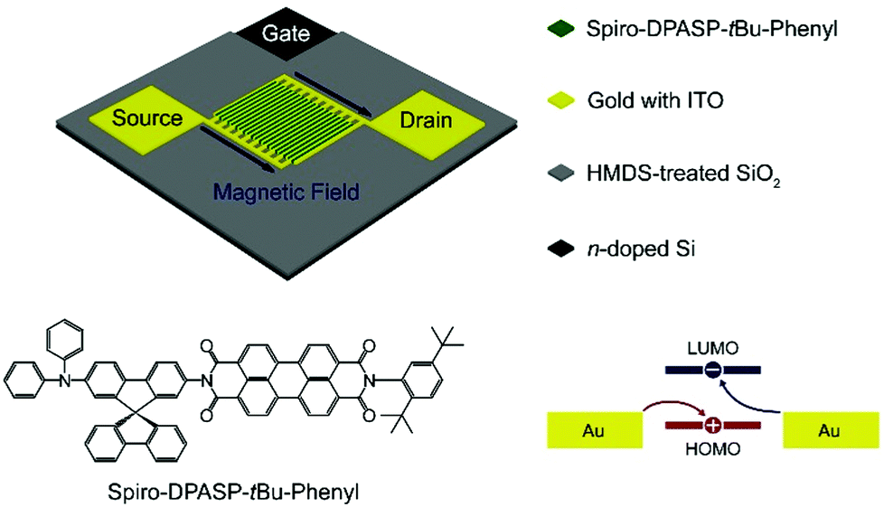 | ||
| Fig. 1 Device architecture and experimental scheme, including the chemical structure of Spiro-DPASP-tBu-phenyl as well as the basic charge injection properties. As sketched based on the HOMO (5.3 eV) and LUMO (3.8 eV) levels and the gold electrodes (work function 5.0 eV). | ||
Spiro-DPASP-tBu-phenyl is thermally stable with a high decomposition temperature of 462 °C, enabling the preparation of vapour-deposited films. It has a glass-like morphology at room temperature and is outstandingly suitable for the construction of optoelectronic devices.28 The frontier energy level of the highest occupied molecular orbital (HOMO) and the lowest unoccupied molecular orbital (LUMO) reflect the properties of the electron donor (arylamine chromophore) and the electron acceptor (perylenetetracarboxylicdiimide chromophore) of the building blocks and give Spiro-DPASP-tBu-phenyl a strong bipolar character. The corresponding HOMO and LUMO values and the injection possibility for electrons and holes are displayed in Fig. 1. The electronic decoupling of the donor and acceptor chromophores lead to an absorption behaviour with two spectrally separated optical bands. Therefore, the absorption spectrum is composed of the UV absorption of the donor-like spiro substituent (bands at 310 nm and 362 nm) and the absorption of the perylenetetracarboxylicdiimide chromophore in the visible wavelength range (bands at 470 nm, 498 nm and 538 nm, see Fig. S1, ESI†).
Fig. 2 shows the current–voltage characteristics of transistors based on Spiro-DPASP-tBu-phenyl with a channel length of 2.5 μm. The non-ideal output curves can be attributed to the short-channel effect and the energy level mismatch between the gold electrode and the HOMO and LUMO levels of Spiro-DPASP-tBu-phenyl. In our opinion, however, a low external magnetic field of <100 mT does not influence the charge injection at the metal/organic interface significantly enough to explain the magnetoresistive behavior of our device. The crossover points in the output characteristics as well as the pronounced “V-like” shape of the transfer curves clearly indicate an ambipolar charge transport behaviour. Therefore, the simultaneous presence of holes and electrons in the conduction channel is most likely23,28 and both types of charge carriers contribute to the drain current Id. We obtained typical linear and saturation regimes as well as an ambipolar charge transport regime, as shown in Fig. 2. An additional charge carrier is injected into the drain-side depletion zone, resulting in the superlinear increase in Id observed in the output characteristics and the characteristic “V-like” shape observed in the transfer curves. The operating regions of ambipolar transistors have been well discussed in the literature.29–31 The charge carrier mobility μ as well as the threshold voltage Vth for both types of charge carriers are determined from the transfer curves according to the equation: Id = WCiμ(Vg − Vth)2/(2L), where W is the channel width, L is the channel length, Ci is the capacitance per unit area, Vd is the drain voltage, Vg is the gate voltage, μ is the mobility and Vth is the threshold voltage. We extracted for holes: μL = 1.6 × 10⁻⁶ cm2 V−1 s−1 and Vth,L = 7.7 V and for electrons: μE = 1.0 × 10⁻⁶ cm2 V−1 s−1 and Vth,L = 60.7 V, respectively. These results indicate balanced charge transport properties for electrons and holes in Spiro-DPASP-tBu-phenyl.
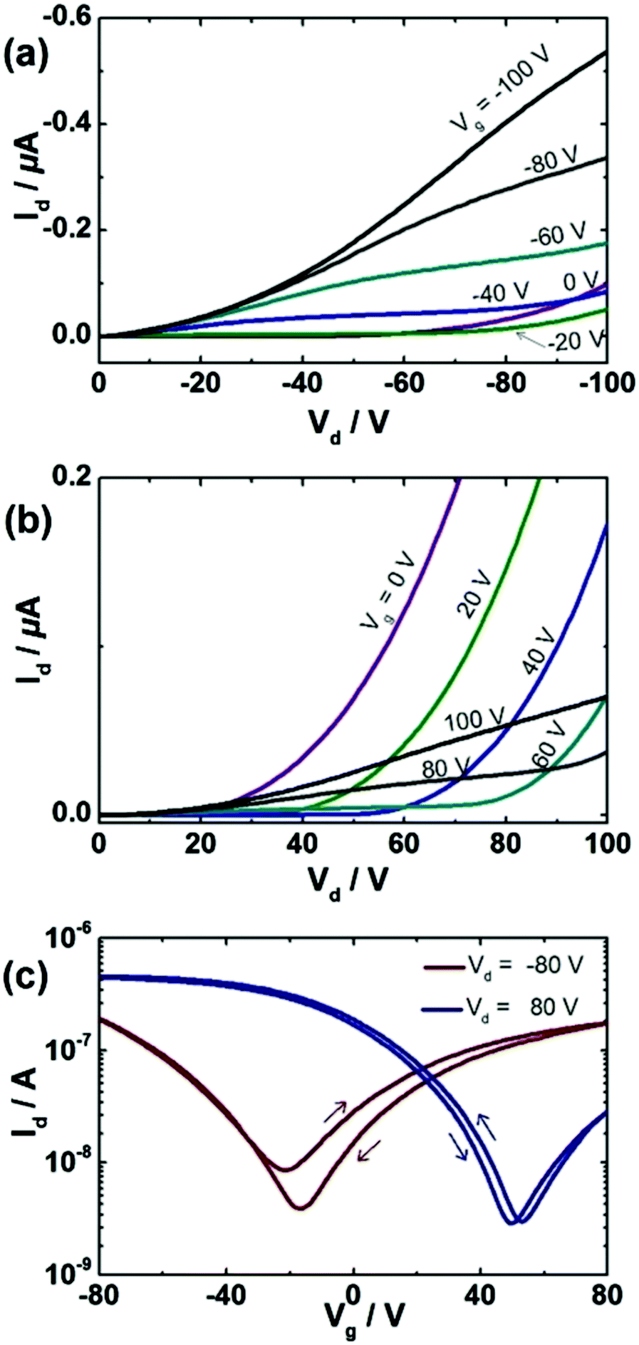 | ||
| Fig. 2 Output curves for p-channel (a) and n-channel (b), respectively. (c) Typical transfer characteristics for ambipolar transistors, featuring a typical “V-like” shape. | ||
Fig. 3 depicts the voltage conditions for three transport regimes: electron-dominated, hole-dominated and ambipolar transport regimes. The borderline between these regimes is determined based on the turn-on voltage of the primary accumulating type of charge carrier as well as the superlinear increase of Id when the secondary charge carriers are injected (see Fig. S2, ESI†). Both effects allow allocating the prevailing charge transport regime within the voltage landscape, as shown in Fig. 3. However, we want to mention that the involvement of a second charge carrier type in the sub-regions of the hole- or electron-dominated regime cannot be completely excluded. Still, our transistors offer the possibility of setting quasi-unipolar or bipolar transport conditions by applying appropriate Vg and Vd.
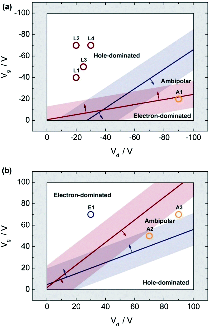 | ||
| Fig. 3 Mapping of the charge transport regimes under (a) p-channel and (b) n-channel conditions, respectively.32 Based on the drain and gate voltages electron-dominated (E), hole-dominated (L) and ambipolar (A) transport regimes can be distinguished. The solid red (holes) and blue (electrons) lines determine the onset of significant contribution of secondarily injected charge carriers to Id. The surrounding, partially transparent areas represent the uncertainty of the determined borderlines. The red and blue arrows indicate the direction within the landscape in which the influence of a charge carrier increases. In addition, voltage-values in hole-dominated (L1–L4), electron-dominated (E1) and ambipolar (A1–A3) transport regions are highlighted in both figures. The points L1–L4, E1 and A1–A3 also denote applied voltages at which magnetotransport measurements have been performed: L1: Vg = −40 V and Vd = −20 V; L2: Vg = −70 V and Vd = −20 V; L3: Vg = −50 V and Vd = −25 V; L4: Vg = −70 V and Vd = −30 V; A1: Vg = −20 V and Vd = −90 V; E1: Vg = 70 V and Vd = 30 V; A2: Vg = 50 V and Vd = 70 V; A3: Vg = 70 V and Vd = 90 V. | ||
The current flow in Spiro-DPASP-tBu-phenyl transistors is influenced by an external magnetic field, as displayed in Fig. 4. Moreover, the sign of the magnetoresistance is strongly affected by Vd as well as Vg. While positive magnetoresistance is achieved for Vd = −20 V and Vg = −70 V, negative magnetoresistance is obtained for Vd = −70 V and Vg = −40 V.
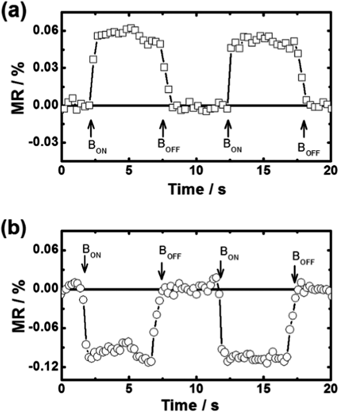 | ||
| Fig. 4 Sign change of magnetoresistance measured at different applied voltages: (a) Vd = −20 V and Vg = −70 V lead to positive magnetoresistance, while (b) Vd = −70 V and Vg = −40 V result in negative magnetoresistance. | ||
Fig. 5 shows the dependency of magnetoresistance on the applied gate and drain voltages for the different transport regimes, including a magnetoresistance sign reversal. Under hole-accumulating conditions (Fig. 5a and c), positive magnetoresistance of up to 0.1% is obtained for a hole-dominated current. Sign reversal of magnetoresistance takes place parallel to the borderlines representing secondary injection of holes and electrons (red and blue lines, as explained in Fig. 3a and Fig. S2, ESI†). The highest negative magnetoresistance of −0.6% can be found within the ambipolar transport regime (see Fig. 5a and c) insinuating a magnetoresistance sign reversal from the unipolar towards the ambipolar regime. An analogous trend can be observed under electron-accumulating conditions (Fig. 5b and d). For an electron-dominated current, positive magnetoresistance of up to 0.5% can be obtained and the highest negative magnetoresistance of −0.5% is allocated in the centre of the ambipolar transport regime. Small deviations occur for biases below 30 V and in the hole-dominated transport regime. Since no measured data could be determined for Vd < 30 V and Vg < 30 V (due to a very low signal-to-noise ratio), the corresponding profile of the magnetoresistance values is mainly determined by the Renka–Cline gridding method used to generate contour maps.32 In addition, a small negative magnetoresistance appears in the hole-dominated transport regime. It is possible that an electron injection takes place earlier, which does not have a significant influence on the current–voltage characteristics, but already has a decisive influence on the magnetoresistance. The negative sign of magnetoresistance in the hole-dominated transport regime would therefore originate from the involvement of magneto-electrically active electrons in the drain current.
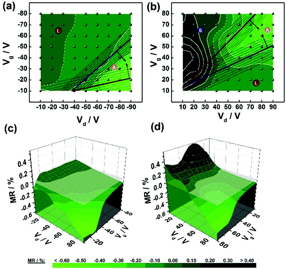 | ||
| Fig. 5 Voltage dependence of magnetoresistance: (a and c) for holes and (b) and (d) for electrons.32 (a and b) present the voltage dependence in a 2D diagram, while (c) and (d) in a 3D contour diagram. The measuring points (different Vg and Vd) are highlighted as dark grey dots in the 2D contour diagrams. To optimize the presentation, the Renka–Cline gridding method was used to interpolate the measurement points. Moreover, hole-dominated, electron-dominated and ambipolar transport regimes are labelled L (red circle), E (blue circle) and A (orange circle), respectively. Their limits are determined by the significant involvement of positive (thick red line) and negative (thick blue line) charge carriers. The surrounding thin lines represent the uncertainty of the determined separation lines. The red (holes) and blue (electron) arrows represent the direction in which the influence of charge carrier type increases. In order to emphasize voltage-induced sign change of magnetoresistance, dashed white lines are introduced in (a) and (b), while grey planes are introduced in (c) and (d). The colour scale of the magnetoresistance values is located in the lower part of the image and applies to all graphs. | ||
Our measurements indicate positive magnetoresistance for the unipolar transport regime and negative magnetoresistance for the ambipolar transport regime. From this trend, the following working hypothesis for the voltage modulation of the magnetoresistive behaviour of Spiro-DPASP-tBu-phenyl transistors is deduced: the voltage-induced sign reversal of magnetoresistance is based on a positive component for electron- or hole-dominated charge transport and a negative component for simultaneous participation of both electrons and holes. By altering the prevailing transport regime via the drain and gate voltages, the sign of the magnetoresistance is altered as well.
To test our working hypothesis we measured the magnetoresistance line shape for the different transport regimes. All data fitted better with a non-Lorentzian function (MR = MR∞B2/(|B| + B0)2 where MR∞ is the MR at infinite B and B0 is the half width at quarter maximum) than with a Lorentzian one (MR = MR∞B2/(|B|2 + B02) where B0 is the half width at half maximum), representatively shown in Fig. S3 (ESI†).33 Magnetoresistance line shapes for the hole-dominated (points: L1, L2, L3 and L4), electron-dominated (point: E1) and ambipolar (points: A1, A2 and A3) charge transport regimes are depicted in Fig. 6. In the unipolar transport regimes, there is always positive magnetoresistance, while in the ambipolar range exclusively negative magnetoresistance prevails. In addition, the line shape in the ambipolar transport regime is slightly broadened with a slower saturation behaviour.
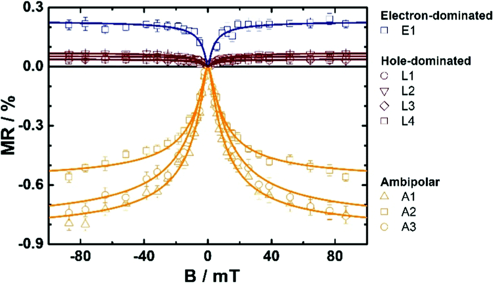 | ||
| Fig. 6 Magnetoresistance values measured at different applied voltages within the electron-dominated, hole-dominated and ambipolar charge transport regimes. The solid lines are non-Lorentzian line shape fits (see text). A clear difference is obtained for unipolar and ambipolar transport regimes regarding the sign as well as the broadness and the saturation behaviour. The points L1–L4, E1 and A1–A3 relate to the Vg and Vd values at which the magnetotransport measurements have been performed: L1: Vg = −40 V and Vd = −20 V; L2: Vg = −70 V and Vd = −20 V; L3: Vg = −50 V and Vd = −25 V; L4: Vg = −70 V and Vd = −30 V; A1: Vg = −20 V and Vd = −90 V; E1: Vg = 70 V and Vd = 30 V; A2: Vg = 50 V and Vd = 70 V; A3: Vg = 70 V and Vd = 90 V. | ||
This qualitative difference between the magnetoresistance line shapes for the unipolar regimes compared to the ambipolar regime is quantified by the fit parameter B0. Fig. S4 (ESI†) summarizes all B0 values determined under hole-dominated, electron-dominated and ambipolar charge transport conditions. Thereby the B0 values for unipolar transport (average value of 2.1 ± 0.4 mT) are significantly lower than the B0 values for ambipolar transport (average value of 5.5 ± 0.5 mT). The value of B0 is often attributed to the strength of the molecular hyperfine fields in which the magnetosensitive quasiparticles are located.7,34–36 Based on the strong bipolar character of Spiro-DPASP-tBu-phenyl, electrons and holes are most likely intramolecularly separated with a high residence probability for positive charge carriers at the arylamine unit (donor character) and a high residence probability for negative charge carriers at the perylenetetracarboxylicdiimide unit (acceptor character). Hence, in Spiro-DPASP-tBu-phenyl, electrons and holes reside in individual hyperfine fields generated by a different (intramolecular) chemical environment. Following this reasoning, one, to a first approximation, can expect that the B0 values for ambipolar charge transport (electrons and holes) are roughly the arithmetic mean of the B0 values for electron-dominated and hole-dominated transport. Since this is not the case, the impact of the hyperfine fields appears not to be suitable to explain the different B0 values. Furthermore, the value of B0 depends on the microscopic details of the corresponding theory used to describe the underlying magnetosensitive mechanism. Therefore, a difference in B0 values for unipolar and ambipolar charge transport implies a specific magnetosensitive mechanism for each of these two transport modes. As conclusion, the positive magnetoresistance under unipolar charge transport conditions and the negative magnetoresistance in the ambipolar regime originate from different magnetosensitive elementary processes. Furthermore, the voltage-induced magnetoresistance sign reversal is based on two different components.
In general, organic magnetoresistance relies on the magnetic-field dependent spin-correlation of particle states, which directly or indirectly influence the charge transport properties of the organic semiconductor.37 Hence, the most important concepts capable of explaining magnetic-field effects in organic materials can be categorized according to the type of (quasi)particle that causes the magnetoresistance. Thereby, the bipolaron model can be applied to elucidate magnetoresistance for unipolar charge transport36 while the electron–hole pair model8 and the exciton–polaron interaction model38,39 can explain magnetoresistance for ambipolar charge transport.
Keeping this in mind, we want to summarize the key features of our results briefly before we address the underlying mechanisms: charge transport in ambipolar Spiro-DPASP-tBu-phenyl transistors can be influenced by external magnetic fields resulting in a magnetoresistance sign reversal (see Fig. 4). The current flow in the conducting channel is divided into hole-dominated, electron-dominated and ambipolar charge transport regimes, which have a correlation with the magnetoresistance landscape as well as the magnetoresistance sign reversal (see Fig. 5). Positive magnetoresistance occurs only under unipolar charge transport conditions while the strongest negative magnetoresistance is most pronounced in the ambipolar regime. Moreover, a significant difference in the form of the line shape is obtained. For unipolar currents, the average line-shape width B0 is 2.1 ± 0.4 mT, while B0 is 5.5 ± 0.5 mT in the ambipolar regime (see Fig. S4, ESI†). The different magnetoresistive properties under unipolar and ambipolar charge transport conditions indicate the existence of two different magnetoresistance components with different signs. The magnetoresistance in Spiro-DPASP-tBu-phenyl is based on a positive component for unipolar charge transport and a negative component for simultaneous participation of electrons and holes in the drain current. Both components are derived from different models.
The bipolaron model can explain the magnetoresistive behaviour for unipolar transport regimes.33,36,37,40 Bipolaron formation is magnetosensitive and the unmodified model causes positive magnetoresistance.33 For the generation of bipolaronic species, the Coulomb repulsion must be overcome.33,36,37,40,41 Both the amorphous morphology of evaporated Spiro-DPASP-tBu-phenyl thin-films28,42 and their bipolar character favour a high degree of energetic disorder and make bipolaron formation realistic. In addition, the high intramolecular difference in electronegativity between the donor and acceptor units in Spiro-DPASP-tBu-phenyl can contribute to the stabilization of bipolaronic states. Therefore, bipolarons are likely to be formed during the charge transport through the amorphous thin-film of Spiro-DPASP-tBu-phenyl.
Due to the quasi-unipolar charge transport as well as the positive magnetoresistance sign, the bipolaron model can be identified as the most likely explanation for the positive magnetoresistance in the hole-dominated and electron-dominated transport regimes of Spiro-DPASP-tBu-phenyl transistors. According to this model, two equilibrated polarons form a bipolaron only in the case of antiparallel spin orientation (singlet configuration). If the spins are aligned parallel (triplet configuration), the so-called spin blockade occurs and no bipolaron is generated.33,40 The bipolaronic singlet and triplet precursor states can be mixed by the statistically distributed hyperfine fields. This spin mixture is magnetosensitive and is reduced in the external magnetic field by the Zeeman splitting. In the magnetic field, therefore, fewer triplets are converted into singlets, resulting in less bipolarons. As a result, more charge carriers are blocked and their mobility is reduced.33,36,40 This results in a bigger resistance and positive magnetoresistance in the unipolar transport regime of Spiro-DPASP-tBu-phenyl transistors.
For ambipolar transport, negative magnetoresistance is obtained, which is based on a different physical mechanism. In this transport regime, holes as well as electrons are present in the conducting channel simultaneously determining the magnetoresistive behaviour. Consequently, electrons and holes interact with a high probability, which can lead to the formation of Coulomb-bound electron–hole pairs (e–h).43 This process can be magnetosensitive and constitutes the origin of negative magnetoresistance in Spiro-DPASP-tBu-phenyl. The spin correlation in e–h pairs is strong enough to result in singlet and triplet states with individual properties, but it does not generate a significant energetic contribution.44,45 Therefore, degenerate singlet and triplet e–h pairs are available in ambipolar transport regimes. These species either dissociate into free charge carriers or recombine into the excitonic state. These reaction pathways have spin-specific recombination rates with singlet e–h pairs having higher recombination rate than triplets.8,46 The conversion of triplets into singlets is controlled by the hyperfine interaction and, thus, it increases the total recombination rate. In the magnetic field, the spin mixture is reduced by the Zeeman splitting and fewer triplets can react via the fast (singlet) reaction path. The overall recombination is reduced, the current flow increases, and negative magnetoresistance is obtained.
Conclusions
We present magnetic-field effects attained in darkness and at low magnetic fields for ambipolar thin-film transistors based on an amorphous low-molecular weight spirobifluorene-bridged bipolar system, namely Spiro-DPASP-tBu-phenyl. The transistors feature distinct unipolar and ambipolar charge transport regimes depending on the applied gate and drain voltages. Thereby, our magnetotransport study reveals a correlation between the charge transport regimes and the magnetoresistive characteristics: positive magnetoresistance prevails in the unipolar regime most likely arising from magnetic-field dependent bipolaron formation. In contrast, we obtain negative magnetoresistance for the ambipolar charge transport regime. This effect can be attributed to magnetic-field dependent recombination rate of e–h pairs. Therefore, there are two magnetoresistance components with opposite sign, which dominate the magnetoresistive behaviour for different charge carrier ratios. The applied drain and gate voltages can control the respective transport regimes and, thus, the sign of the magnetoresistance. Finally, our study shows that amorphous ambipolar organic transistors are not only an interesting platform for the investigation of various magnetic-field effects, but also are promising devices for the development of multifunctional magneto-optoelectronic applications.Experiments
Bottom-contact field-effect transistor substrates were purchased from Fraunhofer IPMS (Dresden, Germany) with channel lengths (L) between 2.5 and 20 μm and a channel width (W) of 10 mm. The isolation layer consists of 230 ± 10 nm thick SiO2 and the source and drain electrodes are 30 nm Au with 10 nm ITO as an adhesion layer. N-[7-(N,N-Diphenylamino)-9,9′-spirobifluoren-2-yl]-N′-(2,5-di-tert-butylphenyl)-3,4:9,10-pery-lenetetracarboxylicdiimide (Spiro-DPASP-tBu-phenyl) was synthesized in our group according to the literature.23 Prior to the deposition of Spiro-DPASP-tBu-phenyl, the predefined substrates were cleaned with acetone, 2-propanol and deionized water, followed by oxygen-plasma treatment and exposure to hexamethyldisilazane (HMDS) to replace the natural hydroxyl end group of SiO2 with an apolar methoxy group. Finally, Spiro-DPASP-tBu-phenyl was deposited by thermal evaporation at a base pressure of 8 × 10⁻⁷ Torr (Tsubstrate = 298 K) with a typical thickness of 35 nm and an evaporation rate of 0.4 Å s−1. The UV/Vis spectrum of the thin-film was measured by using a Perkin-Elmer Lambda 900 UV/Vis/NIR spectrophotometer. From the vacuum chamber, the samples were directly transferred to a glove box (O2, H2O < 0.1 ppm) and placed in a homebuilt sample holder. Current–voltage measurements were carried out by using a Keithley 4200 semiconductor characterization system equipped with preamplifiers for improving low-current measurements. All measurements were performed at room temperature (≈298 K) in darkness. All measurements were carried out for a magnetic field of 60 mT, unless otherwise stated.Acknowledgements
We thank Dr K. Onken for synthesizing the compound. Finally, we are grateful to Prof. J. Salbeck for long-standing support.Notes and references
- Z. H. Xiong, D. Wu, Z. V. Vardeny and J. Shi, Nature, 2004, 427, 821 CrossRef CAS PubMed.
- F. J. Wang, C. G. Yang, Z. V. Vardeny and X. G. Li, Phys. Rev. B: Condens. Matter Mater. Phys., 2007, 75, 245324 CrossRef.
- T. D. Nguyen, E. Ehrenfreund and Z. V. Vardeny, Science, 2012, 337, 204 CrossRef CAS PubMed.
- M. Prezioso, A. Riminucci, I. Bergenti, P. Graziosi, D. Brunel and V. A. Dediu, Adv. Mater., 2011, 23, 1371 CrossRef CAS PubMed.
- M. Gobbi, F. Golmar, R. Llopis, F. Casanova and L. E. Hueso, Adv. Mater., 2011, 23, 1609 CrossRef CAS PubMed.
- J. Kalinowski, M. Cocchi, D. Virgili, P. Di Marco and V. Fattori, Chem. Phys. Lett., 2003, 380, 710 CrossRef CAS.
- Ö. Mermer, G. Veeraraghavan, T. L. Francis, Y. Sheng, D. T. Nguyen, M. Wohlgenannt, A. Köhler, M. K. Al-Suti and M. S. Khan, Phys. Rev. B: Condens. Matter Mater. Phys., 2005, 72, 205202 CrossRef.
- V. N. Prigodin, J. D. Bergeson, D. M. Lincoln and A. J. Epstein, Synth. Met., 2006, 156, 757 CrossRef CAS.
- T. D. Nguyen, Y. Sheng, J. Rybicki and M. Wohlgenannt, Phys. Rev. B: Condens. Matter Mater. Phys., 2008, 77, 235209 CrossRef.
- T. L. Francis, O. Mermer, G. Veeraraghavan and M. Wohlge-nannt, New J. Phys., 2004, 6, 185 CrossRef.
- B. Hu and Y. Wu, Nat. Mater., 2007, 6, 985 CrossRef CAS PubMed.
- F. Wang, F. Macià, M. Wohlgenannt, A. D. Kent and M. E. Flatté, Phys. Rev. X, 2012, 2, 021013 Search PubMed.
- F. Macià, F. Wang, N. J. Harmon, M. Wohlgenannt, A. D. Kent and M. E. Flatté, Appl. Phys. Lett., 2013, 102, 042408 CrossRef.
- M. Nishioka, Y. B. Lee, A. M. Goldman, Y. Xia and C. D. Frisbie, Appl. Phys. Lett., 2007, 91, 092117 CrossRef.
- T. P. I. Saragi and T. Reichert, Appl. Phys. Lett., 2012, 100, 073304 CrossRef.
- T. Reichert and T. P. I. Saragi, Appl. Phys. Lett., 2011, 98, 063307 CrossRef.
- T. Reichert and T. P. I. Saragi, Org. Electron., 2012, 13, 377 CrossRef CAS.
- E. Tatarov, T. Reichert, T. P. I. Saragi, A. Scheffler, R. Ueberschaer, C. Bruhn, T. Fuhrmann-Lieker and J. Salbeck, Chem. Commun., 2013, 49, 4564 RSC.
- T. Reichert, T. P. I. Saragi and J. Salbeck, RSC Adv., 2012, 2, 7388 RSC.
- C. Isenberg and T. P. I. Saragi, J. Mater. Chem. C, 2014, 2, 8569 RSC.
- C. Isenberg, T. Reichert and T. P. I. Saragi, Synth. Met., 2015, 208, 29 CrossRef CAS.
- S. T. Pham, Y. Kawasugi and H. Tada, Appl. Phys. Lett., 2013, 103, 143301 CrossRef.
- K. Onken, PhD thesis, University of Kassel, 2007.
- R. Pudzich, T. Fuhrmann-Lieker and J. Salbeck, Adv. Polym. Sci., 2006, 199, 83 CrossRef CAS.
- E. Shirman, A. Ustinov, N. Ben-Shitrit, H. Weissman, M. A. Iron, R. Cohen and B. Rybtchinski, J. Phys. Chem. B, 2008, 112, 8855 CrossRef CAS PubMed.
- F. Würthner, Chem. Commun., 2004, 1564 RSC.
- H. Langhals, S. Demmig and H. Huber, Spectrochim. Acta, Part A, 1988, 44, 1189 CrossRef.
- T. P. I. Saragi, K. Onken, I. Suske, T. Fuhrmann-Lieker and J. Salbeck, Opt. Mater., 2007, 29, 1332 CrossRef CAS.
- J. Zaumseil and H. Sirringhaus, Chem. Rev., 2007, 107, 1296 CrossRef CAS PubMed.
- E. C. P. Smits, T. D. Anthopoulos, S. Setayesh, E. van Veenendaal, R. Coehoorn, P. W. M. Blom, B. de Boer and D. M. de Leeuw, Phys. Rev. B: Condens. Matter Mater. Phys., 2006, 73, 205316 CrossRef.
- O. Pitayatanakul, T. Higashino, T. Kadoya, M. Tanaka, H. Kojima, M. Ashizawa, T. Kawamoto, H. Matsumoto, K. Ishikawa and T. Mori, J. Mater. Chem. C, 2014, 2, 9311 RSC.
- T. Reichert, PhD thesis, University of Kassel, 2014.
- W. Wagemans and B. Koopmans, Phys. Status Solidi B, 2011, 248, 1029 CrossRef CAS.
- T. D. Nguyen, G. Hukic-Markosian, F. Wang, L. Wojcik, X. G. Li, E. Ehrenfreund and Z. V. Vardeny, Nat. Mater., 2010, 9, 345 CrossRef CAS PubMed.
- R. Giro, F. P. Rosselli, R. dos Santos Carvalho, R. B. Capaz, M. Cremona and C. A. Achete, Phys. Rev. B: Condens. Matter Mater. Phys., 2013, 87, 125204 CrossRef.
- P. A. Bobbert, T. D. Nguyen, F. W. A. van Oost, B. Koopmans and M. Wohlgenannt, Phys. Rev. Lett., 2007, 99, 216801 CrossRef CAS PubMed.
- W. Wagemans, P. Janssen, A. J. Schellekens, F. L. Bloom, P. A. Bobbert and B. Koopmans, SPIN, 2011, 1, 93 CrossRef CAS.
- P. Desai, P. Shakya, T. Kreouzis, W. P. Gillin, N. A. Morley and M. R. J. Gibbs, Phys. Rev. B: Condens. Matter Mater. Phys., 2007, 75, 094423 CrossRef.
- P. Desai, P. Shakya, T. Kreouzis and W. P. Gillin, Phys. Rev. B: Condens. Matter Mater. Phys., 2007, 76, 235202 CrossRef.
- W. Wagemans, F. L. Bloom, P. A. Bobbert, M. Wohlgenannt and B. Koopmans, J. Appl. Phys., 2008, 103, 07F303 CrossRef.
- P. A. Bobbert, T. D. Nguyen, W. Wagemans, F. W. A. van Oost, B. Koopmans and M. Wohlgenannt, Synth. Met., 2010, 160, 223 CrossRef CAS.
- T. P. I. Saragi, T. Spehr, A. Siebert, T. Fuhrmann-Lieker and J. Salbeck, Chem. Rev., 2007, 107, 1011 CrossRef CAS PubMed.
- H. Bässler, Polym. Adv. Technol., 1998, 9, 402 CrossRef.
- M. Segal, M. A. Baldo, R. J. Holmes, S. R. Forrest and Z. G. Soos, Phys. Rev. B: Condens. Matter Mater. Phys., 2003, 68, 075211 CrossRef.
- M. Reufer, M. J. Walter, P. G. Lagoudakis, A. B. Hummel, J. S. Kolb, H. G. Roskos, U. Scherf and J. M. Lupton, Nat. Mater., 2005, 4, 340 CrossRef CAS PubMed.
- J. D. Bergeson, V. N. Prigodin, D. M. Lincoln and A. J. Epstein, Phys. Rev. Lett., 2008, 100, 067201 CrossRef CAS PubMed.
Footnotes |
| † Electronic supplementary information (ESI) available: UV/Vis spectrum, identification of transport regimes, line shape of magnetoresistance and the value of B0 for different transport regimes. See DOI: 10.1039/c7qm00104e |
| ‡ Present address: Accenture GmbH, Kaistraße 20, 40221 Düsseldorf, Germany. |
| This journal is © the Partner Organisations 2017 |